Exciton-phonon coupling induces new pathway for ultrafast intralayer-to-interlayer exciton transition and interlayer charge transfer in WS2-MoS2 heterostructure: a first-principles study
Abstract
Despite the weak, van-der-Waals interlayer coupling, photoinduced charge transfer vertically across atomically thin interfaces can occur within surprisingly fast, sub-50fs timescales. Early theoretical understanding of the charge transfer is based on a noninteracting picture, neglecting excitonic effects that dominate the optical properties of such materials. Here, we employ an ab initio many-body perturbation theory approach which explicitly accounts for the excitons and phonons in the heterostructure. Our large-scale first-principles calculations directly probe the role of exciton-phonon coupling in the charge dynamics of the WS2/MoS2 heterobilayer. We find that the exciton-phonon interaction induced relaxation time of photo-excited excitons at the valley of MoS2 and WS2 is 67 fs and 15 fs at 300 K, respectively, which sets a lower bound to the intralayer-to-interlayer exciton transfer time and is consistent with experiment reports. We further show that electron-hole correlations facilitate novel transfer pathways which are otherwise inaccessible to non-interacting electrons and holes.
The freedom to stack quasi-two-dimensional (quasi-2D) van der Waals (vdW) materials, with little restrictions imposed by lattice matching, introduces a vast parameter space for designing and engineering device properties, as well as exploring new physics by tuning electron correlations and order parameters through proximity effects Geim and Grigorieva (2013). In particular, stacked layers of transition metal dichalcogenides (TMDs) have attracted a lot of interest owing to the unique interplay of spin, valley, and optical chirality properties and promising applications in optoelectronic devices Rivera et al. (2018). TMD heterostructures can form semiconductors with type II band-alignment such that the valence and conduction band edge at their respective points in momentum space have wavefunction characters coming from distinct layers. In this setup, optically excited excitons, which are typically formed by electrons and holes in the same layer, can scatter to lower-energy stable interlayer excitons with longer recombination times. The time scale and microscopic mechanism behind such exciton transfer processes are of fundamental interest and crucial for applications ranging from energy harvesting applications to quantum information sciences Kim et al. (2017).
Recent pump-probe experiments have suggested that for the WS2/MoS2 heterobilayer, such inter-layer charge transfer can take place on a time scale of less than 50 fs Hong et al. (2014). This exceptionally short charge transfer time is surprising, since it is well-understood that the valence band maximum (VBM) and conduction band minimum (CBM) from individual layers – at the point – are only weakly hybridizing. Moreover, phonon modes of the heterostructure also display negligible coupling, apart from very long wavelength acoustic modes. Further, there is a momentum mismatch between the intralayer and interlayer exciton that would prevent a direct Coulomb-mediated charge transfer between the lowest exciton states of the two kind. Later experiments on this system show that this ultrafast transfer is stacking angle independent Yu et al. (2015); Ji et al. (2017); Zhu et al. (2017); Jin et al. (2018) and has a weak dielectric-environment Zhou et al. (2019) dependence. Despite the intense experimental and theoretical efforts Rigosi et al. (2015); Wang et al. (2017), it has so far remained difficult to disentangle the complex experimental observations in vdW heterostructures Schaibley et al. (2016); Chen et al. (2016); Nagler et al. (2017); Bian et al. (2020); Policht et al. (2021) in terms of the competing interaction mechanisms owing in part to the lack of quantitatively predictive ab initio theories that treat vibrational and electronic correlation effects on the same footing.
Earlier theoretical work on WS2/MoS2 heterostructure based on time-dependent density functional theory (TD-DFT) suggested that charge transfer is initiated by coherent charge oscillations and completed by electron-phonon interactions Wang et al. (2016). Non-adiabatic molecular dynamics (NAMD) approaches provided evidence supporting the role of quantum coherence Long and Prezhdo (2016) and electron-phonon interactions Zheng et al. (2018, 2017); Zhang et al. (2017); Wang et al. (2021); Zeng et al. (2021). Excitonic effects have also been incorporated in recent NAMD studies by combining the sampling of the atomic motion from Born-Oppenheimer molecular dynamics with electronic excited-state calculations. The different excited-state potential energy surfaces are approximated either within TD-DFT, using parametrized range-separated hybrid functionals Liu et al. (2020), or within many-body perturbation theory by solving the Bethe-Salpeter equation (BSE) Jiang et al. (2021). In a recent work, a new excitonic channel for intralayer-to-interlayer charge transfers was discovered with TD-aGW calculations Hu et al. (2023). Overall, these calculations uncovered important aspects on the microscopic mechanism beyond independent-particle interlayer charge transfer, and suggest that a two-step relaxation process occurs in the vdW heterostructure, with excitonic effects aiding in the process Liu et al. (2020).
However, while promising, the computational demand of most aforementioned methods is quite steep, and one typically sacrifices the description of electronic correlations to obtain the coupled description of electrons and phonons. For instance, despite earlier pioneering efforts, NAMD calculations are often still restricted to small supercells, which makes the spectrum of excitonic states artificially sparse Qiu et al. (2016), in particular around the energy of intralayer excitons, and may lead to qualitatively different exciton decay pathways.
In this letter, we study exciton transfer (i.e., the rate of scattering from one exciton state to other exciton states via phonons) in a WS2/MoS2 TMD bilayer heterostructure including both electron-hole and exciton-phonon Antonius and Louie (2022); Chen et al. (2020); Huang et al. (2021) interactions fully from first principles within the framework of many-body perturbation theory. Our computed relaxation time of the two lowest-energy intralayer excitons (the A excitons in the two layers) shows that exciton-phonon couplings are capable of inducing ultrafast charge transfer. Moreover, in contrast to the two-step transfer pathway proposed in earlier NAMD studies, we find a direct charge transfer pathway enabled by electron-hole correlations and intravalley scattering, with scattering rates in agreement with the sub-50 fs bleaching of optical signatures seen in experiments Hong et al. (2014); Chen et al. (2016); Ji et al. (2017); Jin et al. (2018). Our direct k-space-resolved exciton and electron dynamics analysis offers a detailed picture of the charge-transfer process.
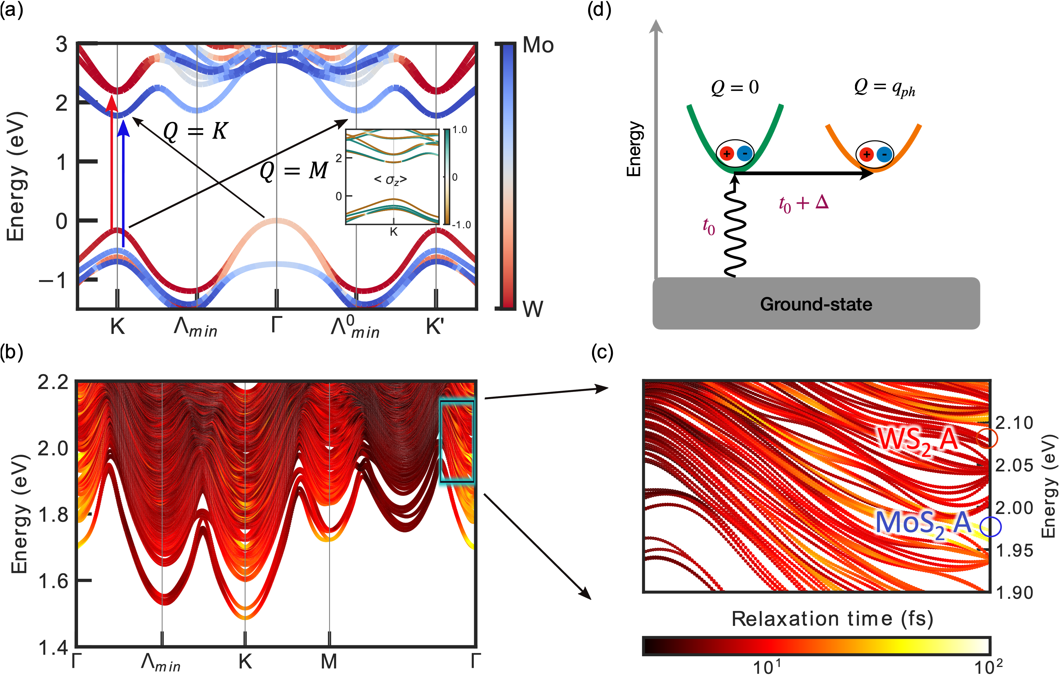
We focus on the energetically favorable H stacking WS2/MoS2 heterostructure, with a twist angle of . Fig. 1 (a) shows the electronic band structure calculated with the G0W0 approach as implemented in the BerkeleyGW software package Hybertsen and Louie (1986); Deslippe et al. (2012). The band structure at the valley clearly exhibits a typical type II band alignment. The first (topmost) valence band at the valley is of WS2 character while the second valence band is of MoS2 character. The next two valence bands also follow the same order. The lowest two conduction bands at the valley both have MoS2 character but opposite spin. The next two conduction bands are of WS2 character. The system is an indirect band-gap semiconductor with the valence band maximum (VBM) at (which is of hybridized characters of the two layers) and the conduction band minimum (CBM) at . The direct band gap is 1.93 eV at the and valleys, where the valence band is about 160 meV lower than the VBM. This energy landscape provides a relaxation path for holes generated in the valley. Furthermore, the mix of Mo and W orbital character at the and valleys suggest an intermediate state that can mediate an intralayer to interlayer charge transfer pathway. In panel (b) we show the exciton dispersion by solving the Bethe-Salpeter equation (BSE) within the GW-BSE method Hybertsen and Louie (1986); Rohlfing and Louie (2000) for excitons with finite center-of-mass (COM) momentum Qiu et al. (2015). Due to the indirect band gap nature, the lowest-energy exciton has a finite COM momentum of and is of interlayer character. Our calculations show that the first intralayer bright exciton in the MoS2 layer has an energy of 1.97 eV and the first intralayer WS2 bright exciton, which must have , is located at 2.09 eV. We will refer to these bright excitons as the MoS2 and WS2 A exciton, respectively. These peaks agree well with previous experiment Hong et al. (2014), within 100 meV, and calculations Torun et al. (2018). We note that both bright excitons lie above the quasiparticle continuum at 1.93 eV of the lower-energy interlayer excitons. Although bound interlayer excitons are abundant below the continuum they only couple weakly to light. In the inset of Fig. 1 (a), we show the quasiparticle bandstructure overlaid with the spin expectation value. The spin-split bands at the valley are a consequence of strong spin-orbit coupling. Due to the spin-polarization near the valley, the bright MoS2 A exciton consists of electrons from the first conduction band and holes from the second valence band, counted from the Fermi energy downward, and the WS2 A exciton consists of electrons from the fourth conduction band and holes from the first valence band. We emphasize that the internal spin structures of each exciton is also relevant to selection rules for exciton-phonon couplings, which is crucial to understand exciton scattering pathways Chan et al. (2023).
Exciton-phonon coupling matrix elements can be written as a contraction of electron-phonon coupling matrix elements with the exciton envelope function given in previous works Toyozawa (1958); Antonius and Louie (2022); Chen et al. (2020); Chan et al. (2023). The lowest-order self-energy due to exciton-phonon couplings reads
| (1) |
where is the exciton energy of a state with quantum number and a COM momentum ; is the phonon frequency; is the Bose-Einstein occupation factor associated with the phonon, is the number of the wavevectors sampled in the Brillouin zone (BZ); and finally, is the exciton-phonon coupling matrix element encoding the probability amplitude for an exciton initially in state () to scatter to state () through the emission or absorption of a phonon . In Fig. 1 (d) we illustrate a typical scattering process which brings an exciton with zero COM momentum to a COM momentum of .
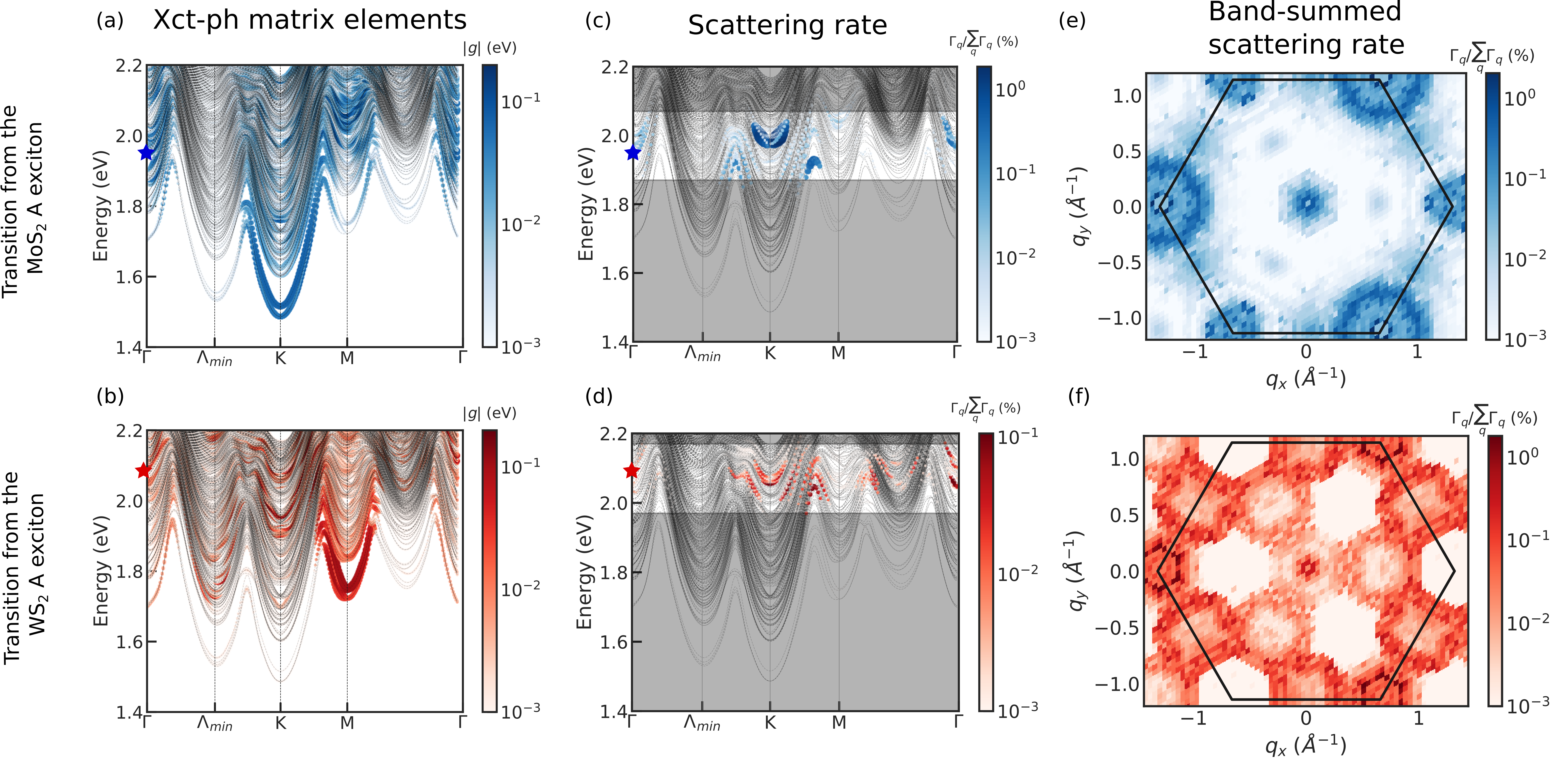
Exciton scattering rates (inverse of the relaxation time) are evaluated from the the imaginary part of on-shell exciton self-energy in Eq. 1. We emphasize this quantity gives the rate of an exciton being scattered from one state to all other states via the exciton-phonon coupling, and it is not between two specific states. In Fig. 1 (b) we show a color map of the exciton-phonon relaxation times in the heterostructure at 300 K. Our calculation shows that the MoS2 A exciton has a relaxation time of 67 fs while WS2 A exciton has a shorter relaxation time of 15 fs. If we take the computed relaxation time to be dominantly due to transitions to exciton states of interlayer character (see below), our results are consistent with the interpretation of the ultrafast charge transfer time observed in the experiments Hong et al. (2014); Chen et al. (2016); Ji et al. (2017); Jin et al. (2018) and with that exciton-phonon interactions dictate the observed ultrafast optical response. Fig. 1 (d) shows a close-up of the region where the two A excitons are located. Since both excitons are in the continuum of the interlayer excitations, one would expect that the available phase space for exciton-phonon scattering is abundant and their relaxation times would be comparable. Yet, we find that the MoS2 A exciton has a relatively long lifetime compared to WS2 A exciton. To understand this result, we analyze momentum and state-resolved exciton-phonon couplings in Fig. 2. In Fig. 2 (a) and (b) we show color maps of the absolute value of band resolved exciton-phonon coupling strength between the MoS2 A exciton and WS2 A exciton and other states summed over all phonon branches. We observe that both excitons are strongly coupled to excitons. Excitons with a COM momentum near also have appreciable coupling matrix elements. excitons consist of electrons at and holes at , which we will denote as pairs while excitons can be either or excitons.
The analysis based purely on exciton-phonon coupling matrix elements does not present a full picture of the relaxation time, which also includes energy conservation (imaginary part of Eq. 1). In Fig. 2 (c) and (d) we show exction states resolved contributions to the scattering rate of the MoS2 (blue star) and WS2 (red star) A excitons along a high symmetry path, respectively. Due to energy conservation conditions, only excitons in the energy window within one phonon frequency can contribute. Hence, for the both layers, the A exciton relaxation time is dominated by scattering from to rather than to , which corresponds to the electron state of the exciton scattering between the and valleys.
We further analyze the scattering rate contributions resolved in the full BZ, as shown in Fig. 2 (e) and (f), which reveals important scattering channels for the MoS2 and WS2 A excitons, respectively, to any excitonic states via absorption and emission of phonons with wavevector . These scattering rates in panels (e) and (f) correspond to the same initial states highlighted with stars in Fig. 2 (c) and (d), respectively. We first study the scattering pathway for an initially excited A exciton in MoS2. We observe that the pattern of contributions to the scattering rate shows a double-ring structure around the valley. For the outer rings, our analysis shows that the final excitons have electrons and holes located mostly at the and points, respectively, (See SM ) indicating that the exciton-phonon scattering was mostly due to a change in the hole momenta. Because the valence states near are layer-hybridized, we conclude that this scattering pathway is important for the ultrafast charge transfer observed in TMDC heterobilayers.
On the other hand, scattering events associated with phonon wavevectors in the inner ring around , are mostly associated with excitons wherein the electrons and holes are distributed at the and valleys, respectively (See SM ). Importantly, we obverse that the final holes change from their original character – mostly MoS2-like at the second valence band at –, to mostly WS2-like at the VBM at . This channel indicates that the MoS2 A exciton can directly couple to interlayer excitons and cause Pauli blocking of the states associated with the WS2 A peak, causing photobleaching of the WS2 absorption signal after the optical pumping of the MoS2 A exciton.
We find that the one-step scattering-event channel associated with the inner ring gives a bleaching time of the WS2 exciton of about 250 fs. On the other hand, we also study a previously discussed two-step scattering mechanism, by which MoS2 A excitons are first scattered to excitons wherein the holes are distributed around to the VBM at (the outer ring process), which subsequently scatters to interlayer excitons. We find that such a two-step process gives a bleaching time of the WS2 exciton of about 200 fs. Similar scattering time was reported in Ref. Wang et al. (2021) for MoSe2/WSe2 bilayer. In Ref Zheng et al. (2018), using non-adiabtic molecular dynamics simulations but neglecting excitonic effects, authors conclude that holes placed in the second valence band at , with initial MoS2 character, relax via both pathways detailed above on timescales of a few hundred femptoseconds. These individual time scales compare well, though are a bit longer than the bleaching time of the WS2 A exciton observed in experiment Hong et al. (2014), and, altogether, strengthen the case that multiple scattering mechanisms are important for ultrafast charge transfer in bilayer MoS2/WS2. We further give a detailed discussion on the temperature dependence of this effect in the supporting information SM .
Next, we focus on the dynamics of the WS2 A exciton. Fig. 2 (f) shows that the WS2 A exciton can scatter by emission or absorption of phonon wavevectors over a larger region of the BZ. In particular, scatterings via phonons with , , and are all viable. Overall, exciton-phonon coupling matrix elements of the MoS2 and WS2 A excitons are of the same order of magnitude; the larger scattering phase space of WS2 A exciton results in its shorter relaxation time.
After showing that exciton-phonon scattering can be fast enough to explain ultrafast charge transfer observed in a WS2/MoS2 heterostructure, an important follow-up question is to microscopically understand how excitons relax after being excited by an optical field and what is the role of electron-hole correlation in that relaxation. Since a full pump-probe simulation including phonons and the exciton relaxation dynamics remains challenging from ab initio many-body perturbation theory, we compute the population redistribution rate of each independent-particle orbital of the many-electron system as an indication of how the carrier population changes as the excitons relax. We define the band- and -resolved quasiparticle redistribution rate of a quasi-electron state with an initially occupied exciton as
| (2) |
where the expectation values are taken over an evolved state starting from either the MoS2 or WS2 A exciton. is the exciton envelope function of a state (,). Here, the scattered exciton COM momentum coincides with phonon momentum since initial A excitons have zero COM momentum. A similar expression of the redistribution rate for valence electrons, along with its derivation, is given in the supporting information SM . In the case with non-degenerate exciton bands at specific , Eq. 2 reduces to
which can be understood as the exciton-phonon scattering rate weighted by the electron or hole components of the exciton envelope functions. In contrast to the independent-particle picture of electron-phonon scattering, we can see from the above expression that different scattering pathways become possible due to the nonlocal distribution of electron or hole amplitude in reciprocal space for excitonic states.
To see the effects of electron-hole interactions in the electron relaxation dynamics, we compare the computed quasi-particle redistribution rate with and without electron-hole interactions in Fig. 3. We show the - and band-resolved distribution of electrons and holes in the bilayer due to the presence of an initial photoexcited A exciton on MoS2 and WS2 in panels (a) and (e), respectively. We show the phonon-induced evolution in occupation of different quasiparticle states, including electron-hole interactions, by plotting in panels (c) and (g), respectively. From Fig. 3 (c), it is clear that, for an initial excitation of the MoS2 A exciton, electrons mostly scatter within the same valley. Intervalley scattering to and a remote occurs with less probability. On the other hand, holes – initially at the second-highest valence band – scatter to both (i) the VBM at and (ii) the two highest-bands in the valley. Since the valley has a mixed character of both W and Mo atoms and the first band in the valley is of W character, both scattering processes (i) and (ii) result in interlayer charge transfers.
We also perform the corresponding calculations without excitonic effects (i.e., considering only electron-phonon interactions). If we start from the lowest-energy vertical transition (intralayer interband transitions) on MoS2 – blue stars in panel (b) – the corresponding quasiparticle scattering rate due to electron-phonon interactions are shown in panel (d). The scattering rate is much more limited in this case owing to the stricter energy-momentum conservation conditions in the non-interacting case. In contrast, excitons with energy close to the MoS2 A exciton can have wide variety of energy and momentum distributions given their different possible internal structure, which allows for the coupling of a variety of states in the BZ. In particular, while holes transfer directly to the VBM at and the valley, it takes a secondary scattering event for this interlayer charge transfer if electron-hole interactions are not taken into account.

For the initially excited WS2 A exciton (Fig. 3 (e)), the redistribution rate in Fig. 3 (g) indicates that scattered electrons have a wider distribution in the BZ than the MoS2 A exciton, which means that electrons are able to move across the whole BZ and is consistent with the analysis in Fig. 2. For holes on the other hand we find that intravalley scattering is preferred. In the free electron-hole picture shown in Fig. 3 (h), we see that scattering of conduction electrons to a remote has a higher intensity, which is a consequence of the stronger electron-phonon coupling between the and the valley. Valence electrons scatter mostly to the side of the valley again due to energy conservation conditions. Comparing these two pictures, we can draw a conclusion that scattering in the exciton picture tends to redistribute charge over a wider range in the BZ, similar to the MoS2 A exciton case. We suggest this is a result of the correlated nature of excitons.
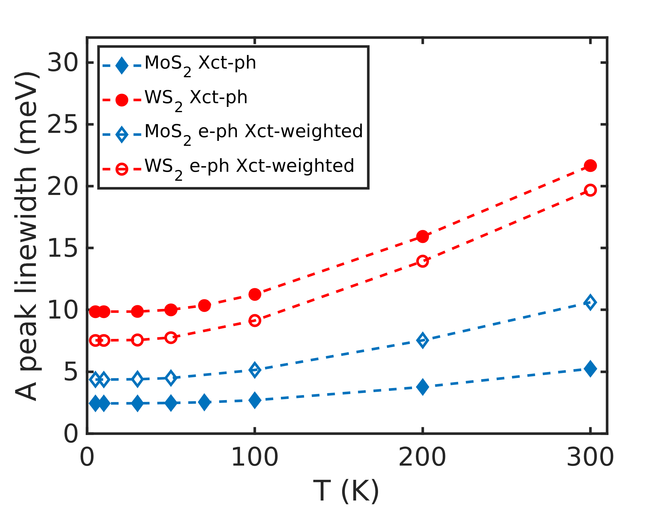
The exciton-phonon coupling strength can be deduced experimentally by measuring the temperature-dependent exciton linewidth. In Fig. 4 we show the linewidths of both MoS2 and WS2 A excitons, which is computed by taking the on-shell imaginary part of the self-energy given by Eq. 1. The exciton-phonon induced linewidth is about 5 meV and 22 meV at 300 K for MoS2 and WS2 A exciton, respectively. To explicitly see the effects of electron-hole interactions, we also compute the linewidth as a linear combination of electron-phonon (and hole-phonon) interaction weighted by the exciton envelope function, which we refer to as the exciton-weighted free electron-hole linewidth Marini (2008); Molina-Sánchez et al. (2016). Although the exciton-phonon linewidth is within the same order of magnitude as that obtained from excited-weighted approach, there is no consistent relation between these two cases. For the MoS2 A exciton, the simpler exciton-weighted electron-phonon linewidth shows a stronger temperature dependence and an overall larger linewidth, while the opposite is true for the for WS2 A exciton. It is therefore necessary to compute exciton-phonon interactions directly for a correct description of exciton relaxations. Finally, we note that the linewidth of the MoS2 A exciton increases to 5 meV in the MoS2/WS2 heterostructure compared to 2 meV in the monolayer at 300 K Chan et al. (2023) while a 26 meV increase was reported in the experiment Rigosi et al. (2015). The underestimation might be owing to the fact that we do not consider defect scatterings and sample inhomogeneity in our calculations.
In conclusion, our first-principles calculations reveal the rich and ultrafast, phonon-mediated exciton scattering channels in a prototypical TMDC bilayer structure of WS2/MoS2. We show that the MoS2 A exciton has a relaxation time of about 67 fs and WS2 has a relaxation time of about 15 fs at 300 K. Moreover, we show that the ultrafast interlayer charge transfer takes place through a multiplicity of channels, and that two-step scattering processes play a significant role: for an initially excited A exciton in MoS2, we predict such channels to cause a photobleaching of the absorption signal at the A exciton resonance in WS2 in about 200 fs. Our band BZ-resolved analysis further reveals that, upon excitation of the MoS2 A exciton, the relaxation primarily involves exciton scatterings which transfer the hole from the point to the region of the BZ while, for the WS2 A excition, it involves the scattering of the electron primarily to a valley around the valley. We expect these findings to inform novel ways of stacking, electronic hybridization, and many-body effects and be synergistically employed to tune charge and energy dynamics in TMDC heterostructures, and that the formalism described here may be used in future studies involving exciton transport in real-time.
Supporting Information. Computational details of GW-BSE, electron-phonon, and exciton-phonon couplings, supplementary figures of phonon dispersion, absorption spectrum, exciton envelope functions, estimation of bleaching time, electron-phonon coupling matrix elements, and derivation of the exciton population change rate.
This work was primarily supported by the Center for Computational Study of Excited State Phenomena in Energy Materials (C2SEPEM), which is funded by the U.S. Department of Energy, Office of Science, Basic Energy Sciences, Materials Sciences and Engineering Division under Contract No. DE-AC02-05CH11231, as part of the Computational Materials Sciences Program. FHJ acknowledges support from the National Science Foundation CAREER award through Grant No. DMR-2238328. Y.-H. C. was supported by the National Science and Technology Council of Taiwan under grant no. 110-2124-M-002-012. We acknowledge the use of computational resources at the National Energy Research Scientific Computing Center (NERSC), a DOE Office of Science User Facility supported by the Office of Science of the U.S. Department of Energy under Contract No. DE-AC02-05CH11231. The authors acknowledge the Texas Advanced Computing Center (TACC) at The University of Texas at Austin and National Center for High-performance Computing (NCHC) in Taiwan for providing HPC resources that have contributed to the research results reported within this paper.
References
References
- Geim and Grigorieva (2013) A. K. Geim and I. V. Grigorieva, “Van der waals heterostructures,” Nature 499, 419–425 (2013).
- Rivera et al. (2018) Pasqual Rivera, Hongyi Yu, Kyle L. Seyler, Nathan P. Wilson, Wang Yao, and Xiaodong Xu, “Interlayer valley excitons in heterobilayers of transition metal dichalcogenides,” Nature Nanotechnology 13, 1004–1015 (2018).
- Kim et al. (2017) Jonghwan Kim, Chenhao Jin, Bin Chen, Hui Cai, Tao Zhao, Puiyee Lee, Salman Kahn, Kenji Watanabe, Takashi Taniguchi, Sefaattin Tongay, Michael F. Crommie, and Feng Wang, “Observation of ultralong valley lifetime in wse¡sub¿2¡/sub¿/mos¡sub¿2¡/sub¿ heterostructures,” Science Advances 3, e1700518 (2017), https://www.science.org/doi/pdf/10.1126/sciadv.1700518 .
- Hong et al. (2014) Xiaoping Hong, Jonghwan Kim, Su-Fei Shi, Yu Zhang, Chenhao Jin, Yinghui Sun, Sefaattin Tongay, Junqiao Wu, Yanfeng Zhang, and Feng Wang, “Ultrafast charge transfer in atomically thin mos2/ws2 heterostructures,” Nature Nanotechnology 9, 682–686 (2014).
- Yu et al. (2015) Yifei Yu, Shi Hu, Liqin Su, Lujun Huang, Yi Liu, Zhenghe Jin, Alexander A. Purezky, David B. Geohegan, Ki Wook Kim, Yong Zhang, and Linyou Cao, “Equally efficient interlayer exciton relaxation and improved absorption in epitaxial and nonepitaxial mos2/ws2 heterostructures,” Nano Lett. 15, 486–491 (2015).
- Ji et al. (2017) Ziheng Ji, Hao Hong, Jin Zhang, Qi Zhang, Wei Huang, Ting Cao, Ruixi Qiao, Can Liu, Jing Liang, Chuanhong Jin, Liying Jiao, Kebin Shi, Sheng Meng, and Kaihui Liu, “Robust stacking-independent ultrafast charge transfer in mos2/ws2 bilayers,” ACS Nano 11, 12020–12026 (2017).
- Zhu et al. (2017) Haiming Zhu, Jue Wang, Zizhou Gong, Young Duck Kim, James Hone, and X.-Y. Zhu, “Interfacial charge transfer circumventing momentum mismatch at two-dimensional van der waals heterojunctions,” Nano Lett. 17, 3591–3598 (2017).
- Jin et al. (2018) Chenhao Jin, Eric Yue Ma, Ouri Karni, Emma C. Regan, Feng Wang, and Tony F. Heinz, “Ultrafast dynamics in van der waals heterostructures,” Nature Nanotechnology 13, 994–1003 (2018).
- Zhou et al. (2019) Hongzhi Zhou, Yida Zhao, and Haiming Zhu, “Dielectric environment-robust ultrafast charge transfer between two atomic layers,” The Journal of Physical Chemistry Letters 10, 150–155 (2019), https://doi.org/10.1021/acs.jpclett.8b03596 .
- Rigosi et al. (2015) Albert F. Rigosi, Heather M. Hill, Yilei Li, Alexey Chernikov, and Tony F. Heinz, “Probing interlayer interactions in transition metal dichalcogenide heterostructures by optical spectroscopy: Mos2/ws2 and mose2/wse2,” Nano Lett. 15, 5033–5038 (2015).
- Wang et al. (2017) Yong Wang, Zhan Wang, Wang Yao, Gui-Bin Liu, and Hongyi Yu, “Interlayer coupling in commensurate and incommensurate bilayer structures of transition-metal dichalcogenides,” Phys. Rev. B 95, 115429 (2017).
- Schaibley et al. (2016) John R. Schaibley, Pasqual Rivera, Hongyi Yu, Kyle L. Seyler, Jiaqiang Yan, David G. Mandrus, Takashi Taniguchi, Kenji Watanabe, Wang Yao, and Xiaodong Xu, “Directional interlayer spin-valley transfer in two-dimensional heterostructures,” Nature Communications 7, 13747 (2016).
- Chen et al. (2016) Hailong Chen, Xiewen Wen, Jing Zhang, Tianmin Wu, Yongji Gong, Xiang Zhang, Jiangtan Yuan, Chongyue Yi, Jun Lou, Pulickel M. Ajayan, Wei Zhuang, Guangyu Zhang, and Junrong Zheng, “Ultrafast formation of interlayer hot excitons in atomically thin mos2/ws2 heterostructures,” Nature Communications 7, 12512 (2016).
- Nagler et al. (2017) Philipp Nagler, Gerd Plechinger, Mariana V Ballottin, Anatolie Mitioglu, Sebastian Meier, Nicola Paradiso, Christoph Strunk, Alexey Chernikov, Peter C M Christianen, Christian Schüller, and Tobias Korn, “Interlayer exciton dynamics in a dichalcogenide monolayer heterostructure,” 4, 025112 (2017).
- Bian et al. (2020) Ang Bian, Dawei He, Shengcai Hao, Yang Fu, Lu Zhang, Jiaqi He, Yongsheng Wang, and Hui Zhao, “Dynamics of charge-transfer excitons in a transition metal dichalcogenide heterostructure,” Nanoscale 12, 8485–8492 (2020).
- Policht et al. (2021) Veronica R. Policht, Mattia Russo, Fang Liu, Chiara Trovatello, Margherita Maiuri, Yusong Bai, Xiaoyang Zhu, Stefano Dal Conte, and Giulio Cerullo, “Dissecting interlayer hole and electron transfer in transition metal dichalcogenide heterostructures via two-dimensional electronic spectroscopy,” Nano Lett. 21, 4738–4743 (2021).
- Wang et al. (2016) Han Wang, Junhyeok Bang, Yiyang Sun, Liangbo Liang, Damien West, Vincent Meunier, and Shengbai Zhang, “The role of collective motion in the ultrafast charge transfer in van der waals heterostructures,” Nature Communications 7, 11504 (2016).
- Long and Prezhdo (2016) Run Long and Oleg V. Prezhdo, “Quantum coherence facilitates efficient charge separation at a mos2/mose2 van der waals junction,” Nano Lett. 16, 1996–2003 (2016).
- Zheng et al. (2018) Qijing Zheng, Yu Xie, Zhenggang Lan, Oleg V. Prezhdo, Wissam A. Saidi, and Jin Zhao, “Phonon-coupled ultrafast interlayer charge oscillation at van der waals heterostructure interfaces,” Phys. Rev. B 97, 205417 (2018).
- Zheng et al. (2017) Qijing Zheng, Wissam A. Saidi, Yu Xie, Zhenggang Lan, Oleg V. Prezhdo, Hrvoje Petek, and Jin Zhao, “Phonon-assisted ultrafast charge transfer at van der waals heterostructure interface,” Nano Lett. 17, 6435–6442 (2017).
- Zhang et al. (2017) Jin Zhang, Hao Hong, Chao Lian, Wei Ma, Xiaozhi Xu, Xu Zhou, Huixia Fu, Kaihui Liu, and Sheng Meng, “Interlayer-state-coupling dependent ultrafast charge transfer in mos2/ws2 bilayers,” Advanced Science 4, 1700086 (2017), https://onlinelibrary.wiley.com/doi/pdf/10.1002/advs.201700086 .
- Wang et al. (2021) Zilong Wang, Patrick Altmann, Christoph Gadermaier, Yating Yang, Wei Li, Lavinia Ghirardini, Chiara Trovatello, Marco Finazzi, Lamberto Duò, Michele Celebrano, Run Long, Deji Akinwande, Oleg V. Prezhdo, Giulio Cerullo, and Stefano Dal Conte, “Phonon-mediated interlayer charge separation and recombination in a mose2/wse2 heterostructure,” Nano Letters 21, 2165–2173 (2021), pMID: 33591207, https://doi.org/10.1021/acs.nanolett.0c04955 .
- Zeng et al. (2021) Huadong Zeng, Xiangyue Liu, Hong Zhang, and Xinlu Cheng, “New theoretical insights into the photoinduced carrier transfer dynamics in ws2/wse2 van der waals heterostructures,” Phys. Chem. Chem. Phys. 23, 694–701 (2021).
- Liu et al. (2020) Junyi Liu, Xu Zhang, and Gang Lu, “Excitonic effect drives ultrafast dynamics in van der waals heterostructures,” Nano Lett. 20, 4631–4637 (2020).
- Jiang et al. (2021) Xiang Jiang, Qijing Zheng, Zhenggang Lan, Wissam A. Saidi, Xinguo Ren, and Jin Zhao, “Real-time ¡i¿gw¡/i¿-bse investigations on spin-valley exciton dynamics in monolayer transition metal dichalcogenide,” Science Advances 7, eabf3759 (2021), https://www.science.org/doi/pdf/10.1126/sciadv.abf3759 .
- Hu et al. (2023) Chen Hu, Mit H. Naik, Yang-hao Chan, and Steven G. Louie, “Excitonic interactions and mechanism for ultrafast interlayer photoexcited response in van der waals heterostructures,” arXiv:2305.17335 (2023).
- Qiu et al. (2016) Diana Y. Qiu, Felipe H. da Jornada, and Steven G. Louie, “Screening and many-body effects in two-dimensional crystals: Monolayer mos2,” Phys. Rev. B 93, 235435 (2016).
- Antonius and Louie (2022) Gabriel Antonius and Steven G. Louie, “Theory of exciton-phonon coupling,” Phys. Rev. B 105, 085111 (2022).
- Chen et al. (2020) Hsiao-Yi Chen, Davide Sangalli, and Marco Bernardi, “Exciton-phonon interaction and relaxation times from first principles,” Phys. Rev. Lett. 125, 107401 (2020).
- Huang et al. (2021) Tianlun Allan Huang, Marios Zacharias, D. Kirk Lewis, Feliciano Giustino, and Sahar Sharifzadeh, “Exciton–Phonon Interactions in Monolayer Germanium Selenide from First Principles,” The Journal of Physical Chemistry Letters 12, 3802–3808 (2021), publisher: American Chemical Society.
- Hybertsen and Louie (1986) Mark S. Hybertsen and Steven G. Louie, “Electron correlation in semiconductors and insulators: Band gaps and quasiparticle energies,” Phys. Rev. B 34, 5390–5413 (1986).
- Deslippe et al. (2012) Jack Deslippe, Georgy Samsonidze, David A. Strubbe, Manish Jain, Marvin L. Cohen, and Steven G. Louie, “Berkeleygw: A massively parallel computer package for the calculation of the quasiparticle and optical properties of materials and nanostructures,” Computer Physics Communications 183, 1269–1289 (2012).
- Rohlfing and Louie (2000) Michael Rohlfing and Steven G. Louie, “Electron-hole excitations and optical spectra from first principles,” Phys. Rev. B 62, 4927–4944 (2000).
- Qiu et al. (2015) Diana Y. Qiu, Ting Cao, and Steven G. Louie, “Nonanalyticity, valley quantum phases, and lightlike exciton dispersion in monolayer transition metal dichalcogenides: Theory and first-principles calculations,” Phys. Rev. Lett. 115, 176801 (2015).
- Torun et al. (2018) Engin Torun, Henrique P. C. Miranda, Alejandro Molina-Sánchez, and Ludger Wirtz, “Interlayer and intralayer excitons in and heterobilayers,” Phys. Rev. B 97, 245427 (2018).
- Chan et al. (2023) Yang-hao Chan, Jonah B. Haber, Mit H. Naik, Jeffrey B. Neaton, Diana Y. Qiu, Felipe H. da Jornada, and Steven G. Louie, “Exciton lifetime and optical line width profile via exciton-phonon interactions: Theory and first-principles calculations for monolayer mos2,” Nano Lett. (2023), 10.1021/acs.nanolett.3c00732.
- Toyozawa (1958) Yutaka Toyozawa, “Theory of Line-Shapes of the Exciton Absorption Bands,” Progress of Theoretical Physics 20, 53–81 (1958), https://academic.oup.com/ptp/article-pdf/20/1/53/5457877/20-1-53.pdf .
- (38) See Supplemental Material at [URL will be inserted by publisher].
- Marini (2008) Andrea Marini, “Ab initio finite-temperature excitons,” Phys. Rev. Lett. 101, 106405 (2008).
- Molina-Sánchez et al. (2016) Alejandro Molina-Sánchez, Maurizia Palummo, Andrea Marini, and Ludger Wirtz, “Temperature-dependent excitonic effects in the optical properties of single-layer ,” Phys. Rev. B 93, 155435 (2016).