LTO-KTO-3interfaces-Suppl6.pdf
Emerging two-dimensional conductivity at Mott-band insulator interface
Abstract
Intriguingly conducting perovskite interfaces between ordinary band insulators are widely explored, whereas similar interfaces with Mott insulators are still not quite understood. Here we address the (001), (110), and (111) interfaces between the LaTiO3 Mott- and large band gap KTaO3 insulators. Based on first-principles calculations, we reveal a mechanism of interfacial conductivity, which is distinct from a formerly studied one applicable to interfaces between polar wide band insulators. Here the key factor causing conductivity is the matching of oxygen octahedra tilting in KTaO3 and LaTiO3 which, due to a small gap in the LaTiO3 results in its sensitivity to the crystal structure, yields metalization of its overlayer and following charge transfer from Ti to Ta. Our findings, also applicable to other Mott insulators interfaces, shed light on the emergence of conductivity observed in LaTiO3/KTaO3 (110) where the ”polar“ arguments are not applicable and on the emergence of superconductivity in these structures.
The formation of a conducting layer at the interface between two insulators is one of the most intriguing problems in the physics of low dimensional electron systems. A remarkable example is the interface between two perovskite band insulators LaAlO3 (LAO) and SrTiO3 (STO) [1, 2]. The electrons at such interface demonstrate high mobility enabling the observation of the Shubnikov-de Haas oscillations and the quantum Hall effect [3, 4, 5]. Moreover, such interface can become superconducting, [6, 7, 8, 9] possibly demonstrating unconventional Cooper pairing produced by the Rashba-like spin-orbit coupling.[10, 11, 12, 13, 14, 15, 16, 17] The understanding, control, and prediction of the emergent phenomena including topological properties, quantum geometries, and superconductivity is vitally related to the mechanism of the conducting layer formation [8, 9, 18, 19, 20, 21, 22].
For oxide electronics, the most prominent mechanism of the conductivity is the so called ”polar catastrophe“, broadly applicable to the (001)-oriented structures [23, 24, 25, 26, 27, 28, 29, 30, 31, 32, 33, 34, 35]. Here, LaAlO3 is essentially thought to consist of oppositely charged layers [LaO]+ and [AlO2]-, while the respective layers of SrTiO3 are electrically neutral. The formation of a polar heterojunction AlO2/LaO/TiO2 eventually results in the electron transfer through the LaAlO3/SrTiO3 interface which causes formation and filling of a conduction band formed by the Ti 3 electron states, responsible for conductivity and, at appropriate conditions, for superconductivity.
Recently, the isostructural perovskite KTaO3 (KTO) attracted a lot of attention due to its ability to produce the surface superconducting state, strongly dependent on the crystal orientation [36, 37, 38, 39, 40, 41, 42, 43]. Band insulator KTaO3 can be brought in contact with Mott insulator LaTiO3 (LTiO) epitaxially grown on its surface with emergence of a conducting LaTiO/KTO interface.[43] Seemingly, it would be straightforward to consider the ”polar catastrophe“ as the mechanism of the formation of the two-dimensional electron gas (2DEG) at the interface and the earlier studies for (001)-oriented LaTiO/KTO found consistency with the mechanism. [25] This approach, however, fails to explain a highly conducting (110)-oriented interface which does not demonstrate the polar discontinuity. Moreover, the observed critical dependence of the interface superconductivity on the LTiO thickness [43] implies that the physics of this Mott insulator is one of the key factors responsible for the interface electronic properties. Thus, another general mechanism of two-dimensional conductivity, possibly applicable to a variety of band-Mott insulator interfaces is needed.
Here we use first-principles calculations to study the formation of interfacial conducting layers for (001), (110), and (111) - oriented LTiO/KTO heterojunctions. We demonstrate that the crystal structure effect, that is the matching in the orientation of the oxygen octahedra surrounding Ti and Ta ions, at the interface and the following charge transfer across the interface are decisive for the formation of conducting layer. This mechanism resulting from a small gap in the LTiO, making it highly sensitive to the crystal structure variations, is distinct from the conventional explanation for polar band insulators and can be extended to other interfaces with Mott insulators.
To have reference points, we present the first-principles calculations of the bulk materials obtained with the Vienna Ab initio Simulation Package (VASP) [44] within the Perdew-Burke-Ernzerhof generalized-gradient approximation [45] (GGA-PBE) for the exchange-correlation potential and implementation of the lattice relaxation. (For technical details see Supplemental Material (SM) [46].) For a band insulator KTO, having the cubic unit cell with the experimental lattice constant Å [47], this approach yields reliably wide gap while the calculated equilibrium volume overestimates slightly its experimental value by . The calculated band gap between Ta 5 and O states exceeds 2 eV.
Calculation of the bulk Mott insulator LTiO within the density functional theory (DFT) needs the DFT+ parametrization [48, 49], i.e. the appropriate correlation parameter applied to the 3 orbitals of Ti. This orthorhombic material with lattice parameters Å and Å has a pseudocubic structure with the lattice constant Å, different by only 0.8 from the of the cubic KTO. This structure is characterized by the tilting angle O (here =Ti), defined as the deviation from the cubic perovskite structure O3, with the experimental value The VASP implementation [50] with the effective eV gives for orthorhombic (Pbnm) LTiO: (i) the band gap of 0.5 eV, (ii) the -type antiferromagnetic structure, and (iii) the Ti magnetic moment of 0.7 in agreement with other numerical approaches.[51, 52] This small 0.5 eV band gap makes the LTiO very sensitive to perturbations and, as we will see, can result in the formation of the 2DEG at the LTiO/KTO interface.
Considering epitaxial interfaces of materials with different lattices, one expects a local modification increasing their similarity, within several atomic layers near the interface. Various structural alterations in similar structures were discussed in experimental and theoretical studies [53, 54, 55, 56, 57, 58, 59], but the tilting of oxygen octahedra has never been considered as the main source for 2DEG formation. However, for small gap materials such as LTiO, this local modification can lead to a sufficient alteration of the electron bands. Since the principal difference between KTO and LTiO is the tilting of the oxygen octahedra, we expect a certain matching of the octahedra tiltings near the interfaces. To clearly show the sensitivity to perturbations in terms of the octahedra tilting, we begin with a computer experiment by calculating the hypothetical cubic LaTiO3 without TiO6 tilting. As this realization is metallic, as shown in the Supplemental Material, we see that the key lattice structural factor of strongly correlated LTiO, keeping its finite small band gap and antiferromagnetism, is the tilting.
To quantitatively understand the critical impact of the tilting on the electronic structure and 2DEG formation, we calculate the bulk electronic and magnetic properties of KTO and LTiO at discrete tilting angles without the following relaxation.
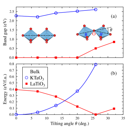
Figure 1 shows the band gap of KTO and LTiO (panel (a)) and its total energy (panel (b)) calculated as a function of With decreasing the LTiO Mott gap decreases and closes for Thus, a small decrease in with respect to its experimental value in LTiO provokes the insulator-to-metal transition. For a wide-band insulator such as KTO or LAO, for comparison, the variation in does not affect significantly the wide gap value. The total energy of LTiO (Fig. 1(b)) shows that robustly metallic LTiO calculated without tilting () is unfavorable by 0.4 eV per the formula unit as compared to the optimally tilted LTiO. We found also that the Ti magnetic moments decrease gradually with decreasing to completely nonmagnetic Ti sites in untilted LTiO. The spin-polarized density of states (DOS) of untilted bulk LTiO is presented in the SM [46] illustrating that this phase is metallic with being about 0.8 eV above the conduction band edge. Thus, if, for certain reasons, the tilting angle in LTiO at the interface decreases compared to the bulk structure, this can cause the 2DEG formation and can be referred to as the ”undertilting“ mechanism of emergence of the conductivity.
We begin with a formal description of the interfaces based on ionic charges. Figure 2 presents the interfacial region of the calculated (001), (110), and (111) LTiO/KTO structures, respectively. Among three interfaces, only the (110) one is unpolar (see Table 1).
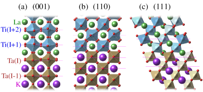
| interface | plane charge sequence | in-plane magnetic order |
|---|---|---|
| (001) | -1/+1/-1/+1//+1/-1/+1/-1 | AFM chessboard |
| (110) | -4/+4/-4/+4//-4/+4/-4/+4 | AFM chains |
| (111) | -5/+5/-5/+5//-3/+3/-3/+3 | FM |
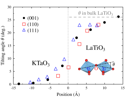
In our main task we study the LTiO/KTO interfaces with first principle calculations. The key feature of the obtained optimized atomic positions and the crystalline structure at the interfaces is the strong layer-dependence of the tilting angles on both LTiO and KTO sides for all considered orientations. Figure 3 shows the calculated tilting angles plotted as a function of the supercell -coordinate. Although the dependence of varies from orientation to orientation, as seen in Fig. 3, the calculations demonstrate that strongly decreases in LTiO toward the interface for all of them. The minimization of the lattice energy tends to match the orientation of the oxygen octahedra in KTO and LTiO at the interface producing KTO-related tilting up to in its interfacial unit cells. Thus, the weak tilting of the oxygen octahedra in LTiO interfacial layers, insufficient to form the Mott insulator, leads to its metalization and formation of the 2DEG at all these interfaces.
Now we consider this interface-based 2DEG in detail. For all considered orientations of interfaces, we found that it is formed mainly by the -type cations, Ta and Ti, placed in the two interfacial unit cells of KTO and LTiO with the spin-polarized DOS calculated for Ta and Ti in the interfacial layers I and I+1 presented in Fig. 4. To compare the Ti and Ta contributions for the three 2DEGs, we calculated for Ta(I) and Ti(I+1) the integrated DOS from the conduction band bottom to the Fermi energy The corresponding charges which are presented in Table 2, show that in LTiO/KTO (001) each interfacial Ta–Ti pair contributes exactly one electron to its 2DEG. Thus, the interface (001) simply closes the gap and transfers the portion of 1/3 from Ti(I+1) to Ta(I). In LTiO/KTO (110) and LTiO/KTO (111), (Ta(I))+(Ti(I+1)) increases to 1.24 and 1.75, respectively. This can be attributed to the increased density of states and to the changes in the number of atomic neighbors, with Ta(I) having one, two, and three Ti(I+1) neighbors at the (001), (110), and (111) interface, respectively. For all the interfaces, occupations of Ta and Ti sites are mutually related due to the common Fermi energy for all electron subbands and the state hybridization. It is interesting to mention that the calculations show the charge ratio for all of the interfaces.
| interface | (Ta(I)) | (Ti(I+1)) | (Ta(I)) | (Ti(I+1)) |
|---|---|---|---|---|
| (001) | 0.32 | 0.67 | 0.68 | 0.43 |
| (110) | 0.39 | 0.85 | 1.10 | 2.03 |
| (111) | 0.58 | 1.17 | 1.52 | 2.40 |
The DOS at the Fermi level of the order of 1 state/eV and charges correspond to a typical metal with the density of the order of one electron per unit cell, in agreement with the experiment.[43, 25] For the (110) and (111) interfaces the DOS at the Fermi level is significantly larger than that at the (001) interface, see Table 2. This difference, which for the (110) interface can be attributed to the anisotropy of the Fermi surface, agrees with the absence of superconductivity in the (001) heterostructures [43] since the DOS at this interface could be not sufficiently large to produce the superconductivity. This argument is generic since a low Fermi level DOS usually disfavors formation of Cooper pairs.
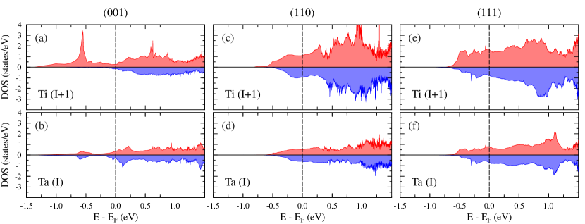
The lower density of states can be attributed to larger interlayer distances in LTiO/KTO (001) heterostructure. This reduces hybridization via the interface, which is reflected in the DOS: the ferromagnetic highly spin-polarized peak at eV below the Fermi level (see Fig. 4(a,b)) corresponding to narrow bands of correlated Ti-based electrons, includes many electron states. Since it pulls electrons below the Fermi level and, thus, decreases the corresponding density of states at the Fermi level as expected for the (001)-related symmetry. In addition to the charge transfer, the proximity with the highly polarized Ti(I+1) magnetic moments induces a weak spin polarization of neighboring Ta with the magnetic moments of the interfacial Ta(I) being about 0.06 (see Sec. III in SM for analysis of atomic configurations at interfaces [46]).
The very similar shapes of their site-projected DOS and similar numerical values, show that the metalization involves Ti and Ta atoms contributions on the same scale, with of Ta states getting a considerable population and becoming conducting together with the contribution of Ti electrons. Thus, the origin of the 2DEG in these systems is different from the case of the LAO/STO (001) interface, in which the 2DEG is formed with the interface polarity accompanied by corresponding band bending.
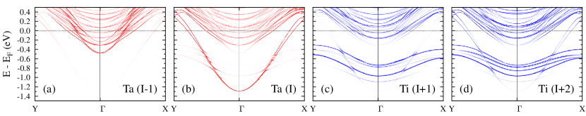
In Fig. 5 each panel shows the energy branches associated with the states of Ta or Ti near the interface. The lowest branches of LTiO/KTO (001) which form its conduction band edge, , belong to the interfacial Ta(I), as Fig. 5(b) shows. Figures 5(a) and 5(b) show the up-shift of the bottom of the corresponding conduction band from Ta(I) to Ta(I-1) layer by approximately 1 eV, indicating a very strong band bending effect, common with the LAO/STO (001). For comparison, the branches of interfacial Ti(I+1) and the next to it Ti(I+2) appear at approximately the same energies, meaning a much weaker band bending effect on this side of the interface, as can be seen in Figs. 5(c) and 5(d). No significant band bending was numerically found at the LTiO/KTO (110) and (111) interfaces. Comparison of Figs. 5(a)-5(d) shows that 2DEG at the LTiO/KTO (001) interface is formed by three different kinds of electron bands: (i) broad Ta-based bands weakly hybridized with the Ti-based ones, demonstrating a considerable band banding and contributing to the formation of the 2DEG, (ii) a large number of narrow Ti-based bands, not crossing the Fermi level, weakly hybridized with the Ta-based ones, and (iii) a large number of considerably hybridized Ti and Ta- based bands crossing the Fermi level. The two latter kinds of bands do not show a strong bending pattern.
Summarizing, the (001), (110), and (111) crystal interfaces between the polar materials such as Mott insulator LaTiO3 and wide band KTaO3 were simulated from the first principles. For all three interfaces we found that their calculated metallic densities of states, formed mostly by the interfacial Ti 3 and Ta 5 states, qualitatively agree with the experimental results. One of key reasons for the formation of two-dimensional metals in all these systems is a strong altering of the oxygen octahedra tilting angles at the interfaces, matching their orientation in KTO and LTiO and considerably decreasing it at the LTiO side compared to the corresponding bulk value. This ”undertilting“ destroys the small LTiO Mott-like band gap at all interfaces (see Figs. 1 and 3), making it the qualitative feature for these systems. At the (001) and (111) interfaces this mechanism can work together with the polarity-induced interface charge transfer making these two effects involving interacting electrons and lattice distortion, inseparable. However, it is important to stress that the appearance of the conducting electrons at the (110) interface cannot be attributed to the polarity (see Table 1) effects and, therefore, the ”undertilting“ is critically important for the conductivity and, at appropriate conditions, for the superconductivity, of this heterostructure. We note that the relatively high density of states of the conducting electrons at the (110) and (111) interfaces can be the decisive factor of their superconductivity in contrast to the (001) interface which is metallic but not superconducting. Another factor which can be detrimental for superconductivity at the (001) interface is the ferromagnetic behavior of interfacial electron states shown in Fig. 4(a). The role of local defects in the 2DEG formation was not considered in our calculations since for the obtained 2DEG at the entire interface area with a large electron concentration and the density of states, a weak disorder in high-quality structures is a marginal effect. [33, 34, 35, 43].
To provide an outlook and further development of this research, we stress that the proposed picture of formation of two-dimensional conducting systems of interacting electrons can be applied to various interfaces between wide gap- and small gap- perovskite Mott insulators. To make this picture applicable, the interface structure should favor tilting of the oxygen octahedra different from that in the bulk Mott insulator with its band structure being strongly sensitive to the tilting, as possibly can occur for thin films of LaVO3 grown on SrTiO3 substrates. [24, 60]
Acknowledgements.
A.E. acknowledges funding by Fonds zur Förderung der Wissenschaftlichen Forschung (FWF) Grant No. I 5384. The work of E.S. is financially supported through Grant No. PID2021-126273NB-I00 funded by MCIN/AEI/10.13039/501100011033 and by ERDF “A way of making Europe,” and by the Basque Government through Grant No. IT1470-22.References
- Ohtomo and Hwang [2004a] A. Ohtomo and H. Y. Hwang, Nature 427, 423 (2004a).
- Thiel et al. [2006] S. Thiel, G. Hammerl, A. Schmehl, C. W. Schneider, and J. Mannhart, Science 313, 1942 (2006).
- Ohtomo and Hwang [2004b] A. Ohtomo and H. Y. Hwang, Nature 427, 423 (2004b).
- McCollam et al. [2014] A. McCollam, S. Wenderich, M. K. Kruize, V. K. Guduru, H. J. A. Molegraaf, M. Huijben, G. Koster, D. H. A. Blank, G. Rijnders, A. Brinkman, H. Hilgenkamp, U. Zeitler, and J. C. Maan, APL Materials 2, 022102 (2014).
- Trier et al. [2016] F. Trier, G. E. D. K. Prawiroatmodjo, Z. Zhong, D. V. Christensen, M. von Soosten, A. Bhowmik, J. M. G. Lastra, Y. Chen, T. S. Jespersen, and N. Pryds, Phys. Rev. Lett. 117, 096804 (2016).
- Reyren et al. [2007] N. Reyren, S. Thiel, A. D. Caviglia, L. F. Kourkoutis, G. Hammerl, C. Richter, C. W. Schneider, T. Kopp, A.-S. Rüetschi, D. Jaccard, M. Gabay, D. A. Muller, J.-M. Triscone, and J. Mannhart, Science 317, 1196 (2007).
- Caviglia et al. [2008] A. D. Caviglia, S. Gariglio, N. Reyren, D. Jaccard, T. Schneider, M. Gabay, S. Thiel, G. Hammerl, J. Mannhart, and J.-M. Triscone, Nature 456, 624 (2008).
- Li et al. [2011] L. Li, C. Richter, J. Mannhart, and R. C. Ashoori, Nature Physics 7, 762 (2011).
- Bert et al. [2011] J. A. Bert, B. Kalisky, C. Bell, M. Kim, Y. Hikita, H. Y. Hwang, and K. A. Moler, Nature Physics 7, 767 (2011).
- Caviglia et al. [2010] A. D. Caviglia, M. Gabay, S. Gariglio, N. Reyren, C. Cancellieri, and J.-M. Triscone, Phys. Rev. Lett. 104, 126803 (2010).
- Ben Shalom et al. [2010] M. Ben Shalom, M. Sachs, D. Rakhmilevitch, A. Palevski, and Y. Dagan, Phys. Rev. Lett. 104, 126802 (2010).
- Bychkov and Rashba [1984] Y. A. Bychkov and E. I. Rashba, Journal of Physics C: Solid State Physics 17, 6039 (1984).
- Venderbos et al. [2018] J. W. F. Venderbos, L. Savary, J. Ruhman, P. A. Lee, and L. Fu, Phys. Rev. X 8, 011029 (2018).
- Gor’kov and Rashba [2001] L. P. Gor’kov and E. I. Rashba, Phys. Rev. Lett. 87, 037004 (2001).
- Scheurer and Schmalian [2014] M. S. Scheurer and J. Schmalian, Nature Communications 6, 6005 (2014).
- Kozii and Fu [2015] V. Kozii and L. Fu, Phys. Rev. Lett. 115, 207002 (2015).
- Nakosai et al. [2012] S. Nakosai, Y. Tanaka, and N. Nagaosa, Phys. Rev. Lett. 108, 147003 (2012).
- Joshua et al. [2013] A. Joshua, J. Ruhman, S. Pecker, E. Altman, and S. Ilani, Proceedings of the National Academy of Sciences 110, 9633 (2013).
- Vaz et al. [2019] D. C. Vaz, P. Noël, A. Johansson, B. Göbel, F. Y. Bruno, G. Singh, S. Mckeown-Walker, F. Trier, L. M. Vicente-Arche, A. Sander, et al., Nature Materials 18, 1187 (2019).
- Lesne et al. [2023] E. Lesne, Y. G. Saǧlam, R. Battilomo, M. T. Mercaldo, T. C. van Thiel, U. Filippozzi, C. Noce, M. Cuoco, G. A. Steele, C. Ortix, and A. D. Caviglia, Nature Materials 22, 576 (2023).
- Gao et al. [2023] A. Gao, Y.-F. Liu, J.-X. Qiu, B. Ghosh, T. V. Trevisan, Y. Onishi, C. Hu, T. Qian, H.-J. Tien, S.-W. Chen, M. Huang, D. Bérubé, H. Li, C. Tzschaschel, T. Dinh, Z. Sun, S.-C. Ho, S.-W. Lien, B. Singh, K. Watanabe, T. Taniguchi, D. C. Bell, H. Lin, T.-R. Chang, C. R. Du, A. Bansil, L. Fu, N. Ni, P. P. Orth, Q. Ma, and S.-Y. Xu, Science 381, 181 (2023).
- Wang et al. [2023] N. Wang, D. Kaplan, Z. Zhang, T. Holder, N. Cao, A. Wang, X. Zhou, F. Zhou, Z. Jiang, C. Zhang, S. Ru, H. Cai, K. Watanabe, T. Taniguchi, B. Yan, and W. Gao, Nature (2023), https://doi.org/10.1038/s41586-023-06363-3 .
- Nakagawa et al. [2006] N. Nakagawa, H. Y. Hwang, and D. A. Muller, Nature Materials 5, 204 (2006).
- Hotta et al. [2007] Y. Hotta, T. Susaki, and H. Y. Hwang, Phys. Rev. Lett. 99, 236805 (2007).
- Zou et al. [2015] K. Zou, S. Ismail-Beigi, K. Kisslinger, X. Shen, D. Su, F. J. Walker, and C. H. Ahn, APL Materials 3, 036104 (2015).
- Biscaras et al. [2010] J. Biscaras, N. Bergeal, A. Kushwaha, T. Wolf, A. Rastogi, R. Budhani, and J. Lesueur, Nature Communications 1, 89 (2010).
- Moetakef et al. [2011] P. Moetakef, T. A. Cain, D. G. Ouellette, J. Y. Zhang, D. O. Klenov, A. Janotti, C. G. Van de Walle, S. Rajan, S. J. Allen, and S. Stemmer, Applied Physics Letters 99, 232116 (2011).
- Al-Tawhid et al. [2021] A. H. Al-Tawhid, D. P. Kumah, and K. Ahadi, Applied Physics Letters 118, 192905 (2021).
- Goniakowski et al. [2008] J. Goniakowski, F. Finocchi, and C. Noguera, Reports on Progress in Physics 71, 016501 (2008).
- Chen et al. [2010] H. Chen, A. M. Kolpak, and S. Ismail-Beigi, Advanced Materials 22, 2881 (2010).
- Bristowe et al. [2014] N. C. Bristowe, P. Ghosez, P. B. Littlewood, and E. Artacho, Journal of Physics: Condensed Matter 26, 143201 (2014).
- Stemmer and Allen [2014] S. Stemmer and S. J. Allen, Annual Review of Materials Research 44, 151 (2014).
- Maznichenko et al. [2018] I. Maznichenko, S. Ostanin, V. Dugaev, I. Mertig, and A. Ernst, Physical Review Materials 2, 074003 (2018).
- Maznichenko et al. [2019] I. Maznichenko, S. Ostanin, A. Ernst, and I. Mertig, Physical Review Materials 3, 074006 (2019).
- Maznichenko et al. [2020] I. V. Maznichenko, S. Ostanin, A. Ernst, J. Henk, and I. Mertig, physica status solidi (b) 257, 1900540 (2020).
- Ueno et al. [2011] K. Ueno, S. Nakamura, H. Shimotani, H. T. Yuan, N. Kimura, T. Nojima, H. Aoki, Y. Iwasa, and M. Kawasaki, Nature Nanotechnology 6, 408 (2011).
- Liu et al. [2021] C. Liu, X. Yan, D. Jin, Y. Ma, H.-W. Hsiao, Y. Lin, T. M. Bretz-Sullivan, X. Zhou, J. Pearson, B. Fisher, J. S. Jiang, W. Han, J.-M. Zuo, J. Wen, D. D. Fong, J. Sun, H. Zhou, and A. Bhattacharya, Science 371, 716 (2021).
- Chen et al. [2021a] Z. Chen, Y. Liu, H. Zhang, Z. Liu, H. Tian, Y. Sun, M. Zhang, Y. Zhou, J. Sun, and Y. Xie, Science 372, 721 (2021a).
- Chen et al. [2021b] Z. Chen, Z. Liu, Y. Sun, X. Chen, Y. Liu, H. Zhang, H. Li, M. Zhang, S. Hong, T. Ren, C. Zhang, H. Tian, Y. Zhou, J. Sun, and Y. Xie, Phys. Rev. Lett. 126, 026802 (2021b).
- Liu et al. [2023] C. Liu, X. Zhou, D. Hong, B. Fisher, H. Zheng, J. Pearson, J. S. Jiang, D. Jin, M. R. Norman, and A. Bhattacharya, Nature Communications 14, 951 (2023).
- Hua et al. [2022] X. Hua, F. Meng, Z. Huang, Z. Li, S. Wang, B. Ge, Z. Xiang, and X. Chen, npj Quantum Materials 7, 97 (2022).
- Arnault et al. [2023] E. G. Arnault, A. H. Al-Tawhid, S. Salmani-Rezaie, D. A. Muller, D. P. Kumah, M. S. Bahramy, G. Finkelstein, and K. Ahadi, Science Advances 9, eadf1414 (2023).
- Maryenko et al. [2023] D. Maryenko, I. Maznichenko, S. Ostanin, M. Kawamura, K. Takahashi, M. Nakamura, V. Dugaev, E. Y. Sherman, A. Ernst, and M. Kawasaki, APL Materials 11, 061102 (2023).
- Kresse and Furthmüller [1996] G. Kresse and J. Furthmüller, Phys. Rev. B 54, 11169 (1996).
- Perdew et al. [1996] J. P. Perdew, K. Burke, and M. Ernzerhof, Phys. Rev. Lett. 77, 3865 (1996).
- [46] Supplemental material, URL_will_be_inserted_by_publisher.
- Tkach et al. [2011] A. Tkach, P. M. Vilarinho, and A. Almeida, Journal of the European Ceramic Society 31, 2303 (2011).
- Anisimov et al. [1991] V. I. Anisimov, J. Zaanen, and O. K. Andersen, Phys. Rev. B 44, 943 (1991).
- Varignon et al. [2019a] J. Varignon, M. Bibes, and A. Zunger, Nature communications 10, 1658 (2019a).
- Rohrbach et al. [2003] A. Rohrbach, J. Hafner, and G. Kresse, Journal of Physics: Condensed Matter 15, 979 (2003).
- Ahn et al. [2006] H.-S. Ahn, D. D. Cuong, J. Lee, and S. Han, Journal of the Korean Physical Society 49, 1536 (2006).
- Varignon et al. [2019b] J. Varignon, M. Bibes, and A. Zunger, Phys. Rev. B 100, 035119 (2019b).
- Ishida and Liebsch [2008] H. Ishida and A. Liebsch, Phys. Rev. B 77, 115350 (2008).
- Okamoto and Millis [2004] S. Okamoto and A. J. Millis, Nature 428, 630 (2004).
- Maurice et al. [2006] J.-L. Maurice, C. Carrétéro, M.-J. Casanove, K. Bouzehouane, S. Guyard, É. Larquet, and J.-P. Contour, physica status solidi (a) 203, 2209 (2006).
- Wong et al. [2010] F. J. Wong, S.-H. Baek, R. V. Chopdekar, V. V. Mehta, H.-W. Jang, C.-B. Eom, and Y. Suzuki, Phys. Rev. B 81, 161101 (2010).
- Okamoto et al. [2006] S. Okamoto, A. J. Millis, and N. A. Spaldin, Phys. Rev. Lett. 97, 056802 (2006).
- Schoofs et al. [2013] F. Schoofs, M. A. Carpenter, M. E. Vickers, M. Egilmez, T. Fix, J. E. Kleibeuker, J. L. MacManus-Driscoll, and M. G. Blamire, Journal of Physics: Condensed Matter 25, 175005 (2013).
- Fister et al. [2014] T. T. Fister, H. Zhou, Z. Luo, S. S. A. Seo, S. O. Hruszkewycz, D. L. Proffit, J. A. Eastman, P. H. Fuoss, P. M. Baldo, H. N. Lee, and D. D. Fong, APL Materials 2, 021102 (2014), https://pubs.aip.org/aip/apm/article-pdf/doi/10.1063/1.4865160/13763179/021102_1_online.pdf .
- Rotella et al. [2012] H. Rotella, U. Lüders, P.-E. Janolin, V. H. Dao, D. Chateigner, R. Feyerherm, E. Dudzik, and W. Prellier, Phys. Rev. B 85, 184101 (2012).