Observation of topological frequency combs
Abstract
On-chip generation of optical frequency combs using nonlinear ring resonators has opened the route to numerous novel applications of combs that were otherwise limited to mode-locked laser systems. Nevertheless, even after more than a decade of development, on-chip nonlinear combs still predominantly rely on the use of single-ring resonators. Recent theoretical investigations have shown that generating combs in a topological array of resonators can provide a new avenue to engineer comb spectra. Here, we experimentally demonstrate the generation of such a novel class of frequency combs, the topological frequency combs, in a two-dimensional (2D) lattice of hundreds of nonlinear ring resonators. Specifically, the lattice hosts topological edge states that exhibit fabrication-robust linear dispersion and spatial confinement at the boundary of the lattice. Upon optical pumping of the topological edge band, these unique properties of the edge states lead to the generation of a frequency comb that is also spectrally confined within the edge band across 40 longitudinal modes. Moreover, using spatial imaging of our topological lattice, we confirm that light generated in the comb teeth is indeed spatially confined at the lattice edge, characteristic of linear topological systems. Our results bring together the fields of topological photonics and optical frequency combs, providing an opportunity to explore the interplay between topology and nonlinear systems in a platform compatible with commercially available nanofabrication processes.
I Introduction
Nonlinear effects, in particular the Kerr effect, in ring resonators provide a compact route to the generation of optical frequency combs in integrated photonic chips [1, 2, 3, 4]. These combs have led to a plethora of applications including spectroscopy [5, 6], precision timekeeping, on-chip signal synthesis, ranging and detection [7, 8], and optical neural networks. While Kerr combs have been demonstrated in a wide variety of integrated material platforms, device design has been predominantly limited to single-ring resonators. Coupled resonator systems have only very recently been investigated as a means to engineer the dispersion, and subsequently, the comb spectrum [9, 10, 11, 12, 13]. Beyond dispersion engineering, nonlinear coupled resonator systems can enable coherent solutions that are not possible using single-ring resonators [14, 15, 16, 13].
Concurrently, topological photonics has emerged as a new and powerful paradigm for the design of photonic devices with novel functionalities [17, 18, 19, 20, 21, 22]. More specifically, topological systems exhibit chiral or helical edge states that are confined to the boundary of the system and are remarkably robust against imperfections common to integrated photonic devices [23, 24, 25]. Examples include robust optical delay lines [26], chiral quantum optics interfaces [27, 28, 29], slow light engineering [30], waveguides, tapers and reconfigurable routers [31, 32, 33]. While early efforts in topological photonics focused on linear devices, more recent demonstrations have included nonlinear effects, extending the scope of possible applications to include lasers [34, 35, 36, 37], parametric amplifiers [38, 39] and quantum light sources [40, 41, 42, 43]. Additionally, it was theoretically shown that nonlinear effects in large two-dimensional (2D) topological arrays of ring resonators can lead to the generation of coherent nested temporal solitons that can exhibit an order of magnitude higher efficiency compared to single-ring combs [44].
Here we experimentally demonstrate the generation of the first topological frequency comb in a 2D lattice of more than ring resonators, fabricated using a commercially available integrated Silicon Nitride (SiN) nanophotonics platform. As we pump within a topological edge band, we observe the generation of a frequency comb confined within the edge bands across 40 longitudinal modes. For a range of pump powers, we observe comb teeth filling the topological edge bandwidth, suggesting the excitation of multiple edge modes in each band, also referred to as “nesting.” Furthermore, we directly image a set of comb teeth and verify that their spatial profile is indeed confined to the edge of the lattice. As such, they constitute a topological edge state that is robust against bends in the lattice and demonstrate the preservation of topology in a highly nonlinear system. This novel modulation instability comb is the first example of a new family of frequency combs and paves the way for the development of coherent topological frequency combs and nested temporal solitons [44].
II Design
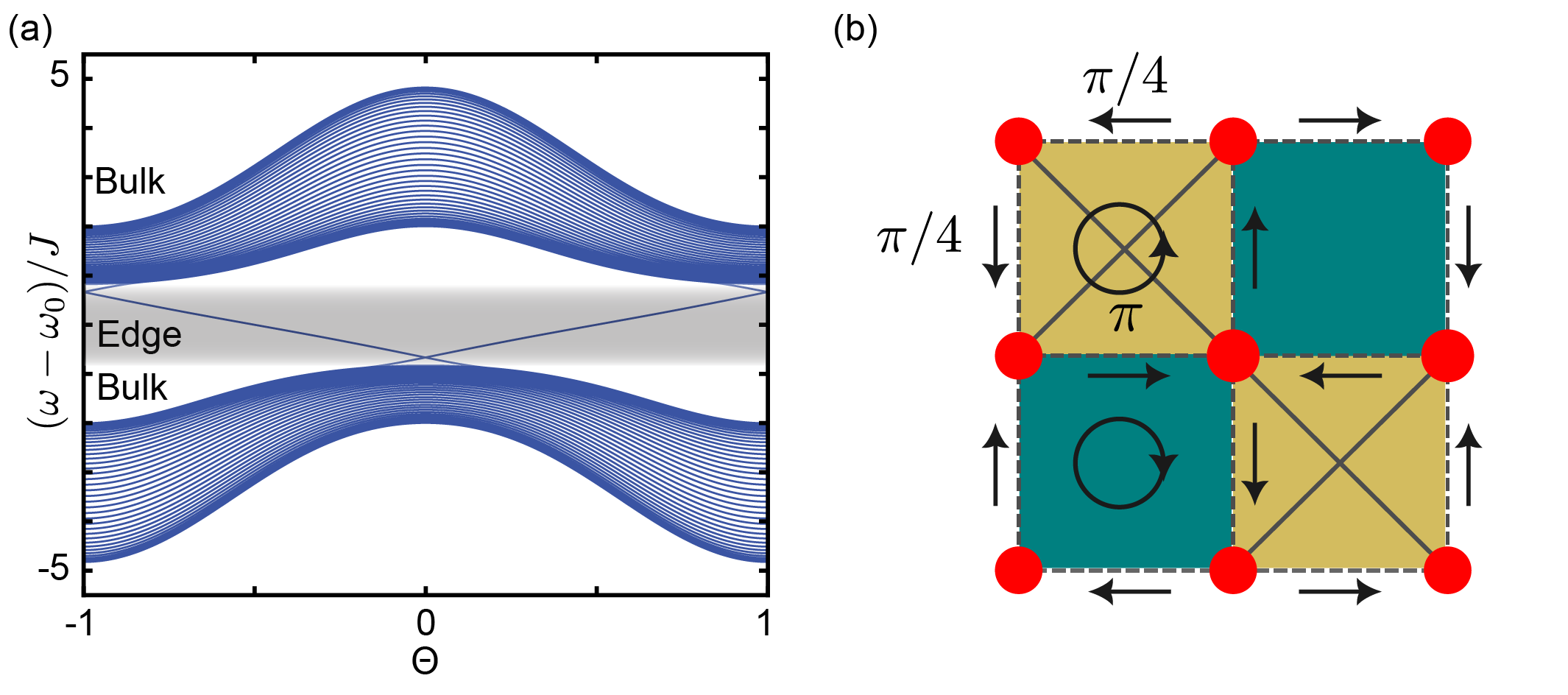
Our topological system consists of an array of coupled ring resonators that simulates the anomalous quantum Hall (AQH) model for photons [45, 46, 44], as shown in Figure 1. The “site-ring” resonators form a square lattice, where nearest and next-nearest sites are coupled together via an interspersed lattice of detuned “link-ring” resonators. The link-rings are detuned by engineering a path-length difference with respect to the site-rings, ensuring that close to site-ring resonances the intensity present in the link-rings will be negligible. As a result, the link-rings act as waveguides and introduce a direction-dependent hopping phase of for nearest-neighbor couplings and for next-nearest neighbor couplings. We note that our system implements a copy of the AQH model at each of the longitudinal mode resonances of the ring resonators. Therefore, the linear dynamics of the system are described by a multi-band tight-binding Hamiltonian ():
| (1) |
Here is the photon creation operator at a site-ring and longitudinal mode . The coupling strength between site-rings for both nearest and next-nearest neighbors is given by . The resonance frequency of the site-ring resonators for a longitudinal mode with index is denoted: where is the free spectral range (FSR) and is the second-order dispersion. This Hamiltonian leads to the existence of an edge band, spectrally located between two bulk bands, near each of the longitudinal mode resonances , as shown in Figure 1. Furthermore, simulated transmission shows each edge band hosting another set of resonances. These resonances are associated with the longitudinal modes of the super-ring resonator formed by the edge states, giving rise to a nested mode structure.
We also emphasize that the system is time-reversal invariant and the topological edge states are helical in nature. More specifically, the clockwise (CW) and counterclockwise (CCW) circulation of light in the site-rings (also referred to as the pseudospin) leads to edge states that are circulating around the lattice boundary in the CCW and CW directions, respectively. By choosing the port of excitation, we can selectively excite a given edge state (Figure 1).
In the presence of a strong pump, the intrinsic Kerr nonlinearity of SiN leads to four-wave mixing, and subsequently, the generation of optical frequency combs in the lattice. This nonlinear interaction is described by the following Hamiltonian:
| (2) |
where is the interaction strength between photons (see SI for definition). Finally, we note that our lattice is a driven-dissipative system. The dissipation includes both the intrinsic decay rate in each individual site, and the extrinsic decay rate introduced by the coupling between input/output rings and probe waveguides, as shown Figure 1. The nonlinear dynamics of this coupled-resonator system is described by a modified Lugiato-Lefever formalism which predicts the formation of nested optical frequency combs [44]. In particular, pumping the lattice in one of the edge bands leads to efficient light generation only in the edge bands centered around other resonances . This is because the spatial confinement of the edge modes ensures significant spatial overlap between different edge modes while minimizing overlap between edge and bulk modes. Furthermore, the linear dispersion of the edge modes ensures that the second-order anomalous dispersion from the waveguides is the dominant contribution as is typical with single-ring combs [44, 40].
III Device Fabrication
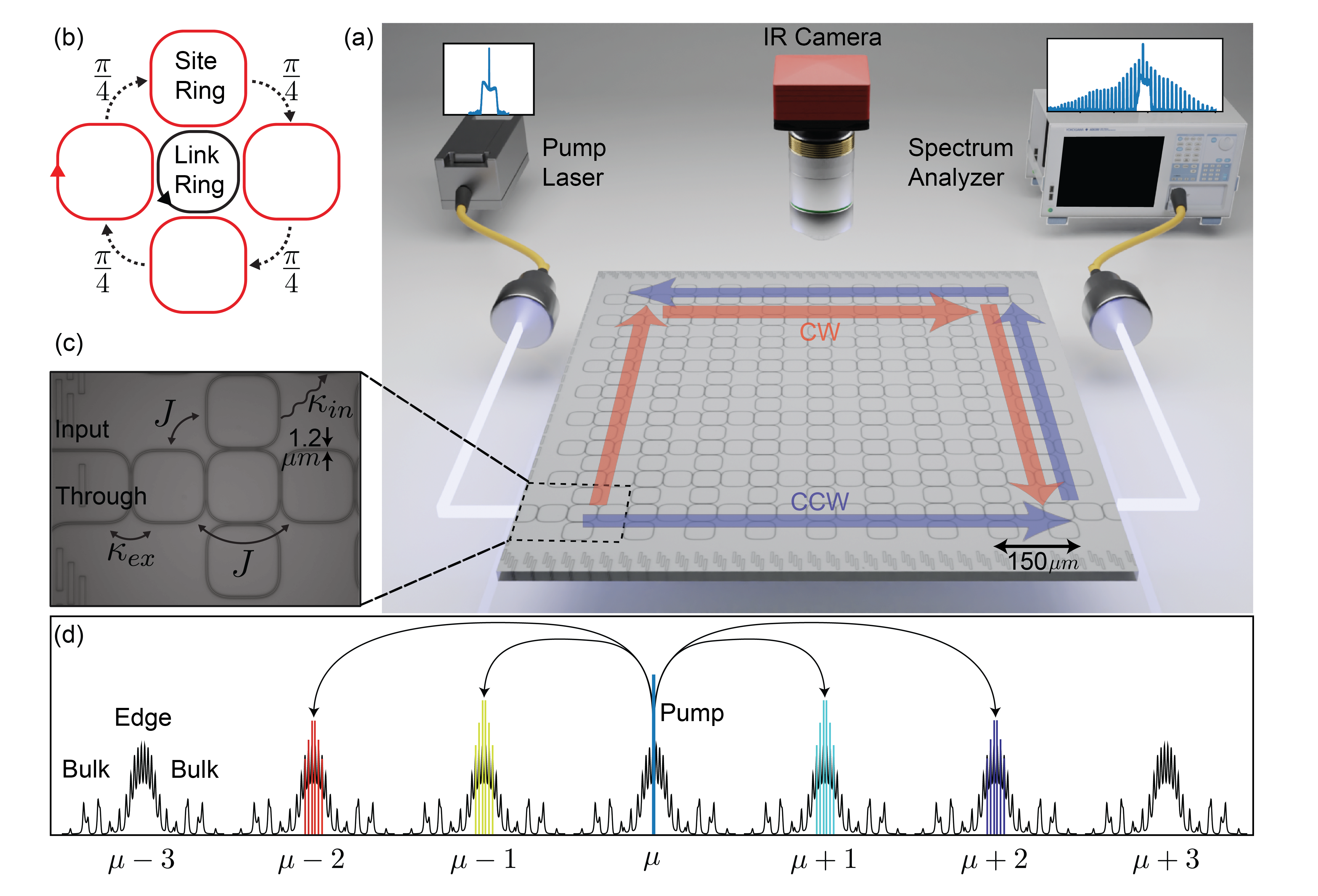
This model is experimentally realized in a thick silicon nitride platform patterned through deep-UV lithography in a commercial foundry [47]. The device itself consists of a 2D array of 261 coupled photonic ring resonators with two coupled input-output waveguides. A high-resolution optical image in Figure 1 shows the topological photonic lattice used in this work. The waveguides are embedded in silicon dioxide and its dimensions are chosen to be 1200 nm wide by 800 nm thick in order to operate in the anomalous dispersion regime. Simulated mode profiles and dispersion can be found in the SI [48]. Each ring is a racetrack design, composed of m straight coupling regions and Euler bend regions with a m effective radius, giving rise to an FSR of THz. Here, we specifically use Euler bends as opposed to round bends to reduce mode mixing that occurs at the straight-bent interfaces within each ring [49]. While this mode-mixing and its impact in perturbing dispersion has also been of concern for single-racetrack combs [50], in our coupled resonator lattice its impact can be physically distinct. In particular, spurious hopping phases can be generated via mode conversion during hopping between adjacent rings [51].
The coupling gaps between the resonators, as well as those between the input-output waveguides and the resonators, are 300 nm, corresponding to an approximate value of GHz for the coupling strength, . The extrinsic and intrinsic couplings ( and ) are estimated to be GHz and GHz, respectively. For details on these calculations, see the SI.
IV Linear Measurements
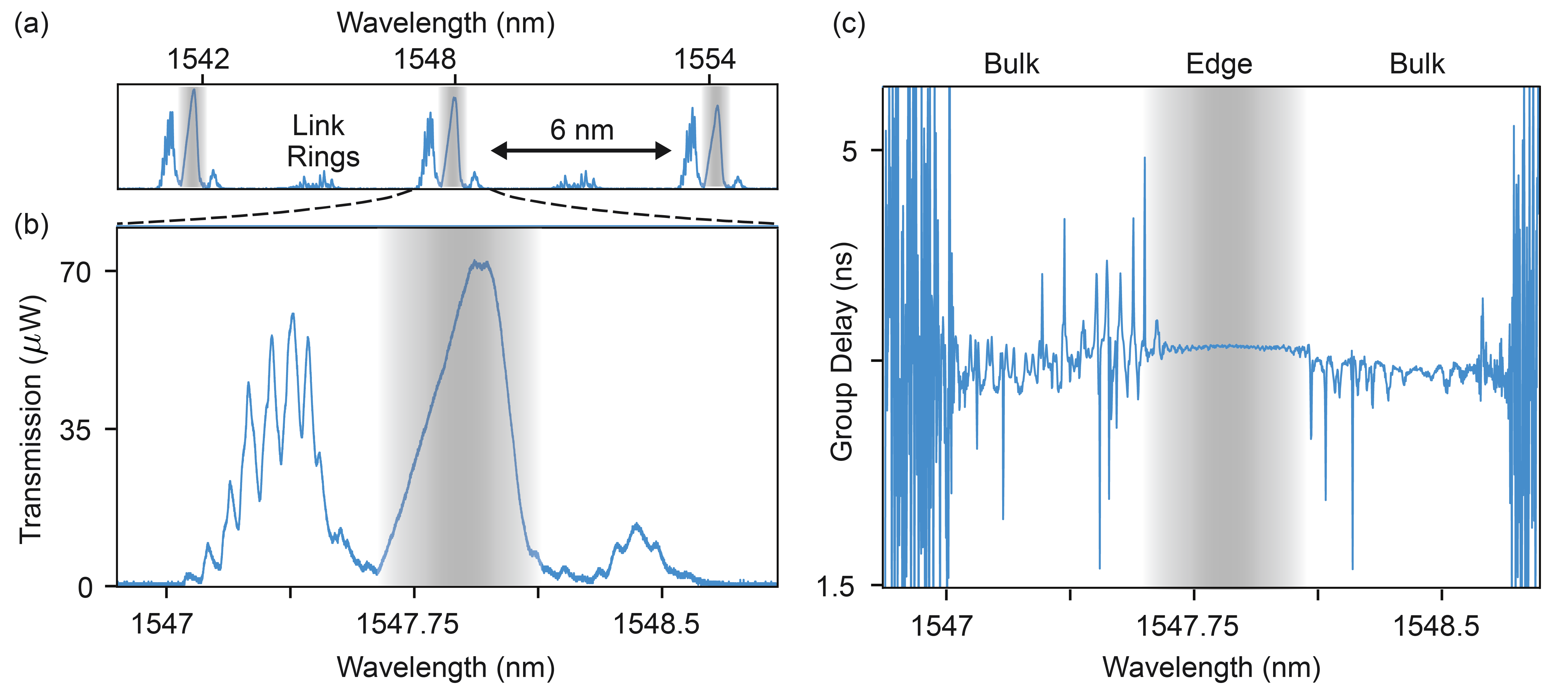
We begin by characterizing the transmission spectrum of the device in the linear (low-power) regime where Kerr phase shifts are negligible. Figure 2 shows the measured transmission spectrum of the device over three longitudinal modes of the site-rings, with a zoomed subset of that spectrum shown. The edge bands are shaded in grey. While the topological edge states are robust against disorders, the bulk states are prone to reduced transmission. We also note that the individual edge state resonances in our experiment are not well resolved due to the fact that the lattice is strongly coupled to input-output waveguides (equivalently, ) and is appreciable.
To highlight the linear dispersion of edge states, we measure the group delay through the lattice, displayed in Figure 2. As expected, the linear dispersion of the edge states leads to a flat delay response in the edge band. The group delay through the bulk states, which do not have a well-defined momentum, shows prominent variations throughout the bulk band.
V Nonlinear Measurements
To observe the formation of topological frequency combs in the ring resonator array, we pump the array using a 5 nanosecond pulsed laser with a repetition rate of 250 kHz and on-chip peak powers up to 100 W. We specifically choose a long pulse laser with a low duty cycle such that we can achieve a high peak power while keeping the average power low enough to avoid serious thermal effects. Furthermore, the 5 ns pulse duration is longer than any relevant timescale of the lattice dynamics, including the round-trip time in the super-ring resonator ( 300 ps). In other words, the longer pulse duration facilitates a selective quasi-continuous wave excitation of the edge band. See SI for additional details of the nonlinear measurement setup and pump laser spectrum.
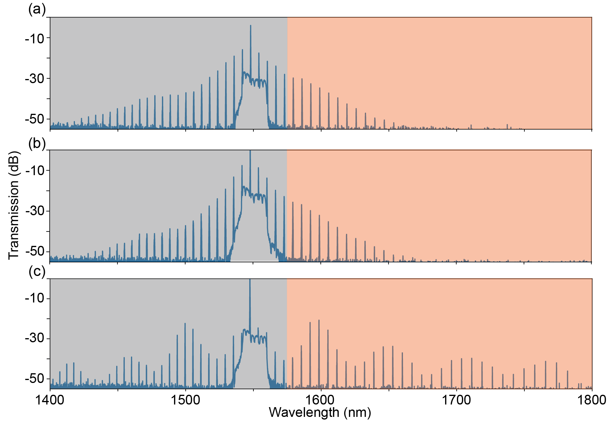
We pump the system at the edge band and show the emergence of the topological frequency comb as a function of increasing pump power. In particular, the spectra displayed in Figure 3 were taken with a pump wavelength of 1547.97 nm and on-chip peak pump powers of {70, 78, 86, 92, and 100} W. The full comb bandwidth at the highest pump power is approximately 250 nm wide with about 65 dB contrast from the most prominent sidebands to the noise floor of the measurement. Insets show zoomed comb spectra for a single longitudinal mode, near 1524 nm, with the grey shaded region indicating the topological edge band. The left inset of panel (e) shows a zoomed region of the spectrum around 1524 nm, spanning five longitudinal modes. The observed FSR of the comb is approximately 6 nm, in agreement with the single-ring FSR.
Additionally, the fact that the comb teeth fill the edge bandwidth and possess a structured spectral envelope is highly suggestive that multiple edge modes within each edge band are oscillating, similar to nesting observed in numerical simulation [44]. However, due to the limited spectral resolution of the measurement ( pm) and the fact that the individual edge modes are poorly resolved even in the linear regime (Figure 2), the exact nature of this potential nesting is not clear.
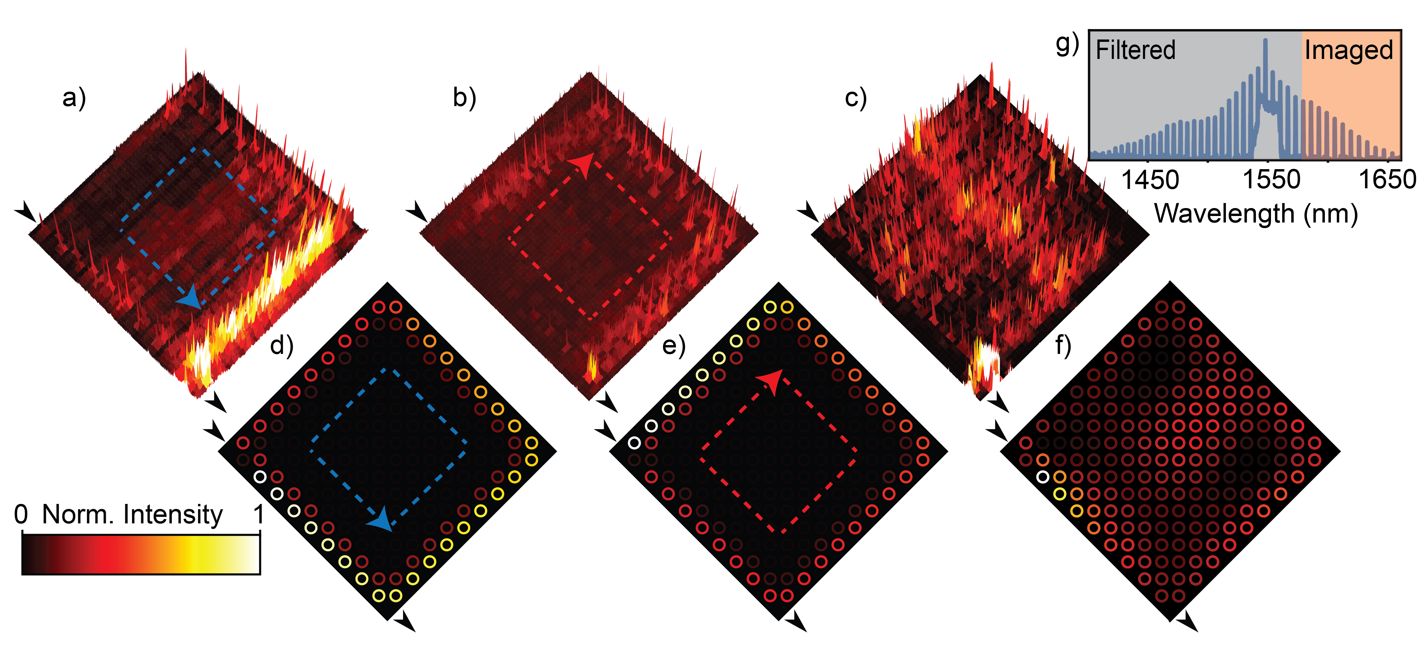
To show that the topological frequency comb inherits the topological properties of the linear system and is indeed confined to the boundary of the lattice, we perform direct imaging of the generated comb. While the system is designed to be well confined in plane, there is a certain amount of out-of-plane scattering caused by fabrication imperfections and disorder. The light scattered due to surface roughness is collected from above with a 10x objective lens and imaged on an infrared (IR) camera. In addition, we use a 1580 nm long-pass filter to remove the pump and only collect part of the generated comb light.
Figure 4 shows the measured spatial intensity profile of three types of generated frequency combs. First, we observe that the generated comb light is confined to the edge of the lattice and light travels from the input to the output port in the CCW direction. Note that the lattice is not critically coupled to the bus waveguides, therefore the light continues to circulate around the lattice after reaching the first output port in its path. Moreover, the propagation is robust and no noticeable scattering into the bulk is observed from the two sharp 90∘ corners. These characteristics show that the comb teeth are indeed generated within the topological edge band and that the topology is preserved even in the presence of strong nonlinearity.
Next, by pumping the system in the other pseudospin, we generate the comb in the CW edge state. We observe similar confinement of the topological frequency comb, but here the light travels in the opposite direction around the lattice, as expected.
In sharp contrast to the CW and CCW edge band excitation, when we excite the lattice in the bulk band, the spatial intensity distribution of generated frequencies exhibits no confinement and occupies the bulk of the lattice. For details on the generation of each of these types of frequency combs, see the SI. Additionally, Figure 4 shows simulated spatial distributions of CCW, CW, and bulk modes in the linear regime for comparison, as well as a schematic illustrating the filtered and imaged regions of the spectrum.
VI Outlook
Here we have demonstrated the first topological frequency comb using an array of more than coupled resonators. Our results entail the first realization of a new class of frequency combs that also includes coherent dissipative solutions, such as nested solitons and phase-locked Turing rolls, that are not accessible using single resonators [44]. In this work we have used a commercially available silicon nitride platform in order to operate in the telecom wavelength regime. However, our device design can be easily translated to other frequency domains and photonic material platforms that can exhibit much higher nonlinearities such as aluminum gallium arsenide [52, 53] and lithium niobate [54]. Such novel multi-resonator combs could enable a host of new application domains to add to those of single and few-resonator frequency combs.
On a more fundamental level, our results provide a new platform to study the interplay of topology and optical nonlinearities [21, 55, 56], as well as intriguing topological physics unique to bosons. For example, while optical nonlinearities have been used to demonstrate topological phase transitions and restructured bulk-edge correspondence [57, 58], here we observe that the system retains the topological behavior of its linear counterpart even in the presence of such strong nonlinear effects. These results could enable novel applications where topological physics is used to engineer the underlying bandstructure (or dispersion) of a linear system and optical nonlinearities provide additional functionalities.
VII Acknowledgements
The authors wish to acknowledge fruitful discussions with Avik Dutt, Rahul Vasanth, Deric Session and Erik Mechtel. This work was supported by AFOSR FA9550-22-1-0339, ONR N00014-20-1-2325, ARL W911NF1920181, NSF DMR-2019444, and Minta Martin and Simons Foundation.
References
- Kippenberg et al. [2011] T. J. Kippenberg, R. Holzwarth, and S. A. Diddams, Science 332, 555 (2011).
- Pasquazi et al. [2018] A. Pasquazi, M. Peccianti, L. Razzari, D. J. Moss, S. Coen, M. Erkintalo, Y. K. Chembo, T. Hansson, S. Wabnitz, P. Del’Haye, X. Xue, A. M. Weiner, and R. Morandotti, Phys. Rep. 729, 1 (2018).
- Gaeta et al. [2019] A. L. Gaeta, M. Lipson, and T. J. Kippenberg, Nat. Photonics 13, 158 (2019).
- Diddams et al. [2020] S. A. Diddams, K. Vahala, and T. Udem, Science 369, eaay3676 (2020).
- Suh et al. [2016] M.-G. Suh, Q.-F. Yang, K. Y. Yang, X. Yi, and K. J. Vahala, Science 354, 600 (2016).
- Long et al. [2023] D. A. Long, M. J. Cich, C. Mathurin, A. T. Heiniger, G. C. Mathews, A. Frymire, and G. B. Rieker, Nature Photonics , 1 (2023).
- Riemensberger et al. [2020] J. Riemensberger, A. Lukashchuk, M. Karpov, W. Weng, E. Lucas, J. Liu, and T. J. Kippenberg, Nature 581, 164 (2020).
- Chen et al. [2023] R. Chen, H. Shu, B. Shen, L. Chang, W. Xie, W. Liao, Z. Tao, J. E. Bowers, and X. Wang, Nature Photonics 17, 306 (2023).
- Miller et al. [2015] S. A. Miller, Y. Okawachi, S. Ramelow, K. Luke, A. Dutt, A. Farsi, A. L. Gaeta, and M. Lipson, Opt. Express 23, 21527 (2015).
- Kim et al. [2017] S. Kim, K. Han, C. Wang, J. A. Jaramillo-Villegas, X. Xue, C. Bao, Y. Xuan, D. E. Leaird, A. M. Weiner, and M. Qi, Nature Communications 8, 372 (2017).
- Bao et al. [2019] H. Bao, A. Cooper, M. Rowley, L. Di Lauro, J. S. Totero Gongora, S. T. Chu, B. E. Little, G.-L. Oppo, R. Morandotti, D. J. Moss, B. Wetzel, M. Peccianti, and A. Pasquazi, Nat. Photonics 13, 384 (2019).
- Xue et al. [2019] X. Xue, X. Zheng, and B. Zhou, Nat. Photonics 13, 616 (2019).
- Yuan et al. [2023] Z. Yuan, M. Gao, Y. Yu, H. Wang, W. Jin, Q.-X. Ji, A. Feshali, M. Paniccia, J. Bowers, and K. Vahala, Nature Photonics 17, 977 (2023).
- Vasco and Savona [2019] J. Vasco and V. Savona, Phys. Rev. Applied 12, 064065 (2019).
- Tikan et al. [2021] A. Tikan, J. Riemensberger, K. Komagata, S. Hönl, M. Churaev, C. Skehan, H. Guo, R. N. Wang, J. Liu, P. Seidler, et al., Nature Physics 17, 604 (2021).
- Tusnin et al. [2023] A. Tusnin, A. Tikan, K. Komagata, and T. J. Kippenberg, Communications Physics 6, 1 (2023).
- Lu et al. [2014] L. Lu, J. D. Joannopoulos, and M. Soljačić, Nature photonics 8, 821 (2014).
- Ozawa et al. [2019] T. Ozawa, H. M. Price, A. Amo, N. Goldman, M. Hafezi, L. Lu, M. C. Rechtsman, D. Schuster, J. Simon, O. Zilberberg, et al., Reviews of Modern Physics 91, 015006 (2019).
- Price et al. [2022] H. Price, Y. Chong, A. Khanikaev, H. Schomerus, L. J. Maczewsky, M. Kremer, M. Heinrich, A. Szameit, O. Zilberberg, Y. Yang, et al., Journal of Physics: Photonics 4, 032501 (2022).
- Zhang et al. [2023] X. Zhang, F. Zangeneh-Nejad, Z.-G. Chen, M.-H. Lu, and J. Christensen, Nature 618, 687 (2023).
- Smirnova et al. [2020] D. Smirnova, D. Leykam, Y. Chong, and Y. Kivshar, Applied Physics Reviews 7 (2020).
- Jalali Mehrabad et al. [2023] M. Jalali Mehrabad, S. Mittal, and M. Hafezi, Phys. Rev. A 108, 040101 (2023).
- Wang et al. [2009] Z. Wang, Y. Chong, J. D. Joannopoulos, and M. Soljacić, Nature 461, 772 (2009).
- Rechtsman et al. [2013] M. C. Rechtsman, J. M. Zeuner, Y. Plotnik, Y. Lumer, D. Podolsky, F. Dreisow, S. Nolte, M. Segev, and A. Szameit, Nature 496, 196 (2013).
- Hafezi et al. [2013] M. Hafezi, S. Mittal, J. Fan, A. Migdall, and J. M. Taylor, Nature Photonics 7, 1001 (2013).
- Mittal et al. [2014] S. Mittal, J. Fan, S. Faez, A. Migdall, J. M. Taylor, and M. Hafezi, Physical review letters 113, 087403 (2014).
- Barik et al. [2018] S. Barik, A. Karasahin, C. Flower, T. Cai, H. Miyake, W. DeGottardi, M. Hafezi, and E. Waks, Science 359, 666 (2018).
- Mehrabad et al. [2023] M. J. Mehrabad, A. Foster, N. Martin, R. Dost, E. Clarke, P. Patil, M. Skolnick, and L. Wilson, Optica 10, 415 (2023).
- Guddala et al. [2021] S. Guddala, F. Komissarenko, S. Kiriushechkina, A. Vakulenko, M. Li, V. Menon, A. Alù, and A. Khanikaev, Science 374, 225 (2021).
- Guglielmon and Rechtsman [2019] J. Guglielmon and M. C. Rechtsman, Physical Review Letters 122, 153904 (2019).
- Shalaev et al. [2019] M. I. Shalaev, W. Walasik, A. Tsukernik, Y. Xu, and N. M. Litchinitser, Nature Nanotechnology 14, 31 (2019).
- Flower et al. [2023] C. J. Flower, S. Barik, M. J. Mehrabad, N. J. Martin, S. Mittal, and M. Hafezi, ACS Photonics 10, 3502 (2023).
- Zhao et al. [2019] H. Zhao, X. Qiao, T. Wu, B. Midya, S. Longhi, and L. Feng, Science 365, 1163 (2019).
- St-Jean et al. [2017] P. St-Jean, V. Goblot, E. Galopin, A. Lemaître, T. Ozawa, L. Le Gratiet, I. Sagnes, J. Bloch, and A. Amo, Nat. Photonics 11, 651 (2017).
- Bahari et al. [2017] B. Bahari, A. Ndao, F. Vallini, A. El Amili, Y. Fainman, and B. Kanté, Science 358, 636 (2017).
- Bandres et al. [2018] M. A. Bandres, S. Wittek, G. Harari, M. Parto, J. Ren, M. Segev, D. N. Christodoulides, and M. Khajavikhan, Science 359 (2018).
- Yang et al. [2022] L. Yang, G. Li, X. Gao, and L. Lu, Nat. Photonics 16, 279–283 (2022).
- Peano et al. [2016] V. Peano, M. Houde, F. Marquardt, and A. A. Clerk, Physical Review X 6, 041026 (2016).
- Sohn et al. [2022] B.-U. Sohn, Y.-X. Huang, J. W. Choi, G. F. Chen, D. K. Ng, S. A. Yang, and D. T. Tan, Nature Communications 13, 7218 (2022).
- Mittal et al. [2018] S. Mittal, E. A. Goldschmidt, and M. Hafezi, Nature 561, 502 (2018).
- Blanco-Redondo et al. [2018] A. Blanco-Redondo, B. Bell, D. Oren, B. J. Eggleton, and M. Segev, Science 362, 568 (2018).
- Mittal et al. [2021a] S. Mittal, V. V. Orre, E. A. Goldschmidt, and M. Hafezi, Nat. Photonics 15, 542 (2021a).
- Dai et al. [2022] T. Dai, Y. Ao, J. Bao, J. Mao, Y. Chi, Z. Fu, Y. You, X. Chen, C. Zhai, B. Tang, Y. Yang, Z. Li, L. Yuan, F. Gao, X. Lin, M. G. Thompson, J. L. O’Brien, Y. Li, X. Hu, Q. Gong, and J. Wang, Nat. Photonics 16, 248 (2022).
- Mittal et al. [2021b] S. Mittal, G. Moille, K. Srinivasan, Y. K. Chembo, and M. Hafezi, Nature Physics 17, 1169 (2021b).
- Leykam et al. [2018] D. Leykam, S. Mittal, M. Hafezi, and Y. D. Chong, Physical review letters 121, 023901 (2018).
- Mittal et al. [2019] S. Mittal, V. V. Orre, D. Leykam, Y. D. Chong, and M. Hafezi, Physical review letters 123, 043201 (2019).
- Rahim et al. [2019] A. Rahim, J. Goyvaerts, B. Szelag, J.-M. Fedeli, P. Absil, T. Aalto, M. Harjanne, C. Littlejohns, G. Reed, G. Winzer, S. Lischke, L. Zimmermann, D. Knoll, D. Geuzebroek, A. Leinse, M. Geiselmann, M. Zervas, H. Jans, A. Stassen, C. Domínguez, P. Muñoz, D. Domenech, A. L. Giesecke, M. C. Lemme, and R. Baets, IEEE Journal of Selected Topics in Quantum Electronics 25, 1 (2019).
- Luke et al. [2015] K. Luke, Y. Okawachi, M. R. E. Lamont, A. L. Gaeta, and M. Lipson, Opt. Lett. 40, 4823 (2015).
- Fujisawa et al. [2017] T. Fujisawa, S. Makino, T. Sato, and K. Saitoh, Optics Express 25, 9150 (2017).
- Ji et al. [2022] X. Ji, J. Liu, J. He, et al., nonlinear photonic integrated circuits. Commun Phys 5 (2022).
- Tzuang et al. [2014] L. D. Tzuang, K. Fang, P. Nussenzveig, S. Fan, and M. Lipson, Nature photonics 8, 701 (2014).
- Chang et al. [2020] L. Chang, W. Xie, H. Shu, Q.-F. Yang, B. Shen, A. Boes, J. D. Peters, W. Jin, C. Xiang, S. Liu, et al., Nature communications 11, 1331 (2020).
- Pu et al. [2016] M. Pu, L. Ottaviano, E. Semenova, and K. Yvind, Optica 3, 823 (2016).
- Zhang et al. [2019] M. Zhang, B. Buscaino, C. Wang, A. Shams-Ansari, C. Reimer, R. Zhu, J. M. Kahn, and M. Lončar, Nature 568, 373 (2019).
- Jürgensen et al. [2021] M. Jürgensen, S. Mukherjee, and M. C. Rechtsman, Nature 596, 63 (2021).
- Mostaan et al. [2022] N. Mostaan, F. Grusdt, and N. Goldman, Nature Communications 13, 5997 (2022).
- Maczewsky et al. [2020] L. J. Maczewsky, M. Heinrich, M. Kremer, S. K. Ivanov, M. Ehrhardt, F. Martinez, Y. V. Kartashov, V. V. Konotop, L. Torner, D. Bauer, and A. Szameit, Science 370, 701 (2020).
- Kirsch et al. [2021] M. S. Kirsch, Y. Zhang, M. Kremer, L. J. Maczewsky, S. K. Ivanov, Y. V. Kartashov, L. Torner, D. Bauer, A. Szameit, and M. Heinrich, Nat. Phys. 17, 995 (2021).
- Ikeda et al. [2008] K. Ikeda, R. E. Saperstein, N. Alic, and Y. Fainman, Opt. Express 16, 12987 (2008).
VIII Supplementary Information
VIII.1 Measurement Setup and Methods
For measurements in the linear regime, we couple a continuous-wave tunable laser to the input port (via edge couplers) and sweep the wavelength. Concurrently, the output power is measured at the drop port across the lattice with a power meter. For the measurement of the group delay of the drop port transmission, we use an optical vector network analyzer. In both cases, polarization is controlled with a standard 3-paddle polarization controller at the laser output.
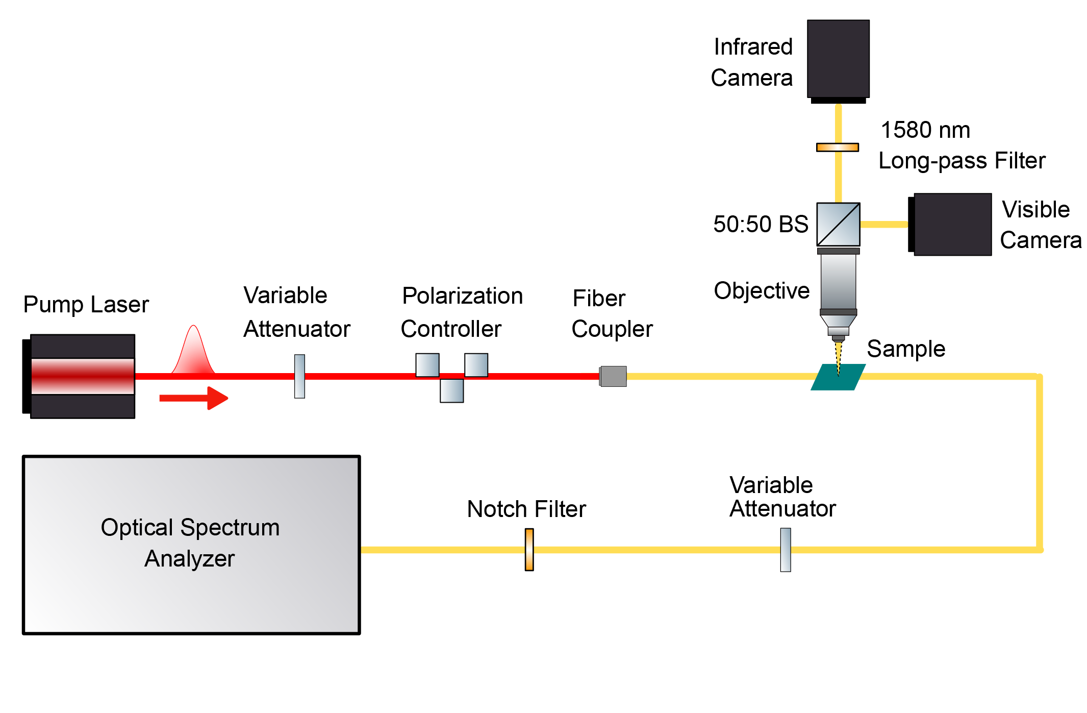
A schematic of the experimental setup for nonlinear measurement is shown in Figure S1. For these measurements, we couple a pulsed tunable laser to a free-space optical setup including a variable attenuator and a polarization controller comprised of a quarter, half, and quarter wave-plate. The output is then coupled into a short tapered fiber and edge coupled into the SiN chip via the input port. The pump and comb output are collected from the drop port with another tapered fiber and optionally attenuated or filtered prior to being sent into an optical spectrum analyzer.
For imaging, we collect out-of-plane scattering from the SiN chip with a 10x objective lens. The image is sent through a 50:50 beamsplitter to a visible wavelength camera as well as an infrared (IR) sensitive camera. A 1580 nm long-pass filter is included prior to the IR camera to filter out the pump laser.
VIII.2 Estimation of Device Parameters
The relevant parameters used in theoretical modeling are estimated from our device as follows. , the coupling strength between rings is estimated by comparing the measured drop spectrum of the lattice with simulation in the linear regime. The full bandwidth of edge and bulk bands is estimated to be approximately 8 in simulation, while the edge band alone is approximately 2. Using this, we arrive at an estimate of 25 GHz for our device.
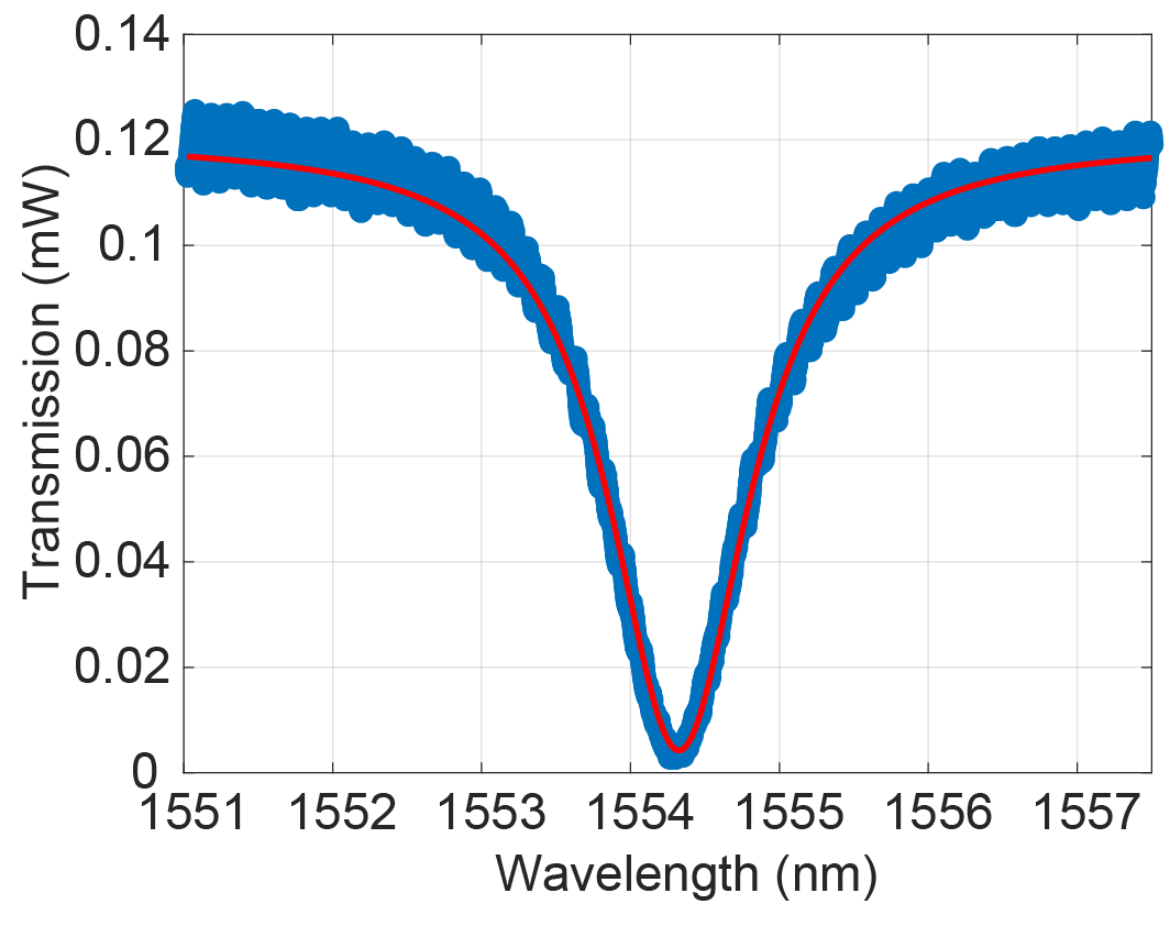
The extrinsic coupling rate and the intrinsic decay rate are estimated based on single-rings coupled to two waveguides, also known as add-drop filters (ADFs). Using the single mode approximation, the transmission spectrum of the through port of an ADF with a given and is a Lorentzian function:
| (S1) |
Here () is the extrinsic coupling to the input (output) waveguide. In the case of our lattice, due to identical coupling gaps, . By measuring the transmission from the through port (see Figure S2) and fitting the curve to the above Lorentzian we extract the values 30 GHz and 2 GHz. This corresponds to a single-ring loaded quality factor of about 1500.
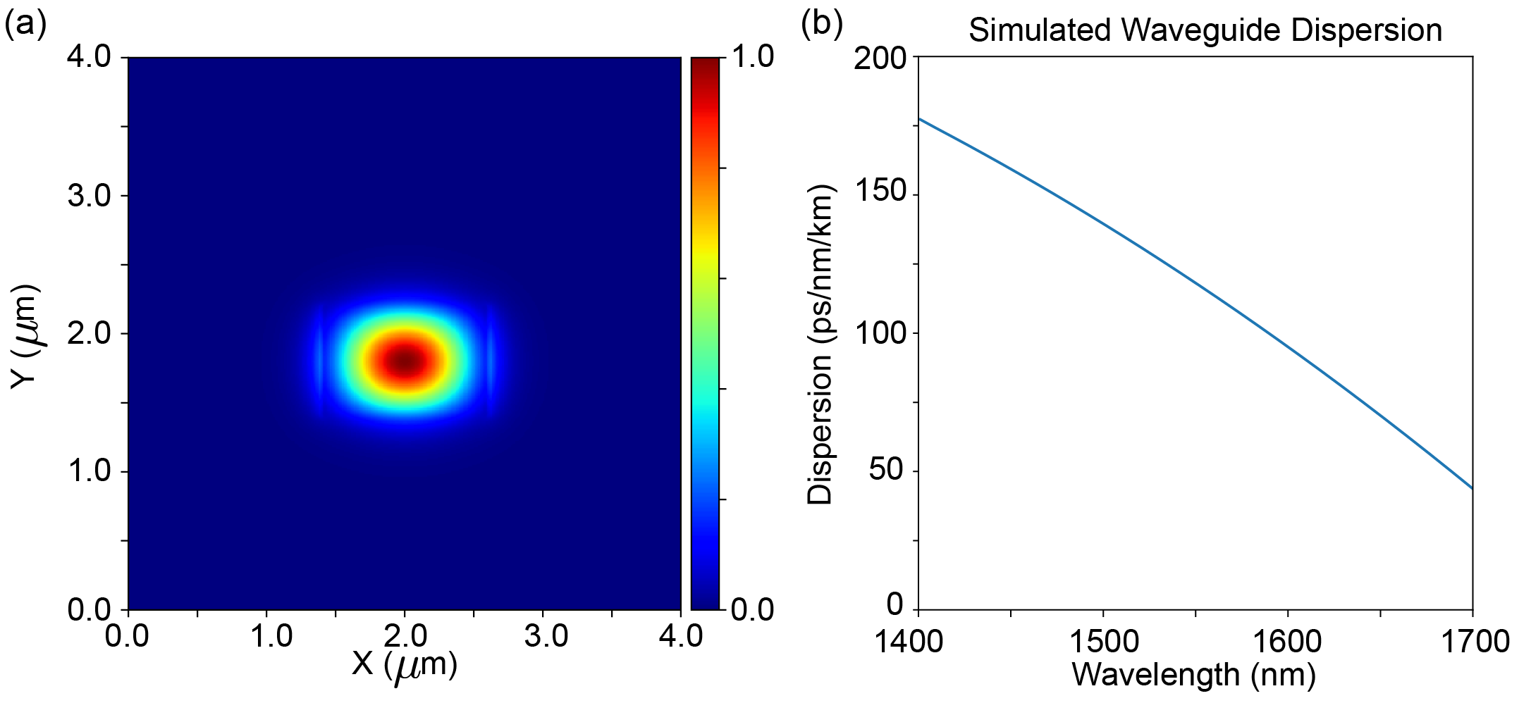
In our second quantized formalism, the strength of interaction is related to the effective Kerr nonlinear strength common in the literature as , where is the refractive index, is the circumference of the individual ring, and is the pump frequency. In order to estimate , we also require the nonlinear index and the effective mode area . Here, a value of m2 W-1 is used [59]. The refractive index of SiN at a wavelength of 1550 nm is taken as [48]. A value of m2 was calculated using FDTD simulation and . With these values, we calculate as:
| (S2) |
We note that the definition of effective Kerr nonlinear strength in this paper is common in the literature but differs from what was used in reference [44], in which it was taken as . The simulated mode profile and dispersion are displayed in Figure S3, using the dependence of the refractive index on wavelength reported in [48].
VIII.3 Band Structure
Figure S4 shows the calculated band structure of a semi-infinite (periodic in one axis, finite in the other) AQH lattice. A -wide edge band region (highlighted in grey) resides between two bulk bands. Unlike the bulk modes, which lack well-defined momentum, there are two unidirectional edge bands with opposite pseudospins. These bands travel in opposite directions and are robust against local disorder. [45, 46]. Additionally, the lattice unit cell is depicted schematically.
VIII.4 Pump Laser Characterization
The pump laser used in the nonlinear measurements described in this work is a tunable pulsed laser. The pulse duration is designed to be approximately 5 ns with a repetition rate of 250 kHz. This relatively long pulse duration (compared to the longest timescales of the lattice dynamics) and low repetition rate provide access to a high power quasi-continuous wave regime. In particular, operation in this regime allows power requirements to be satisfied and detrimental thermal effects to be minimized while numerical modeling using a single frequency pump remains applicable.
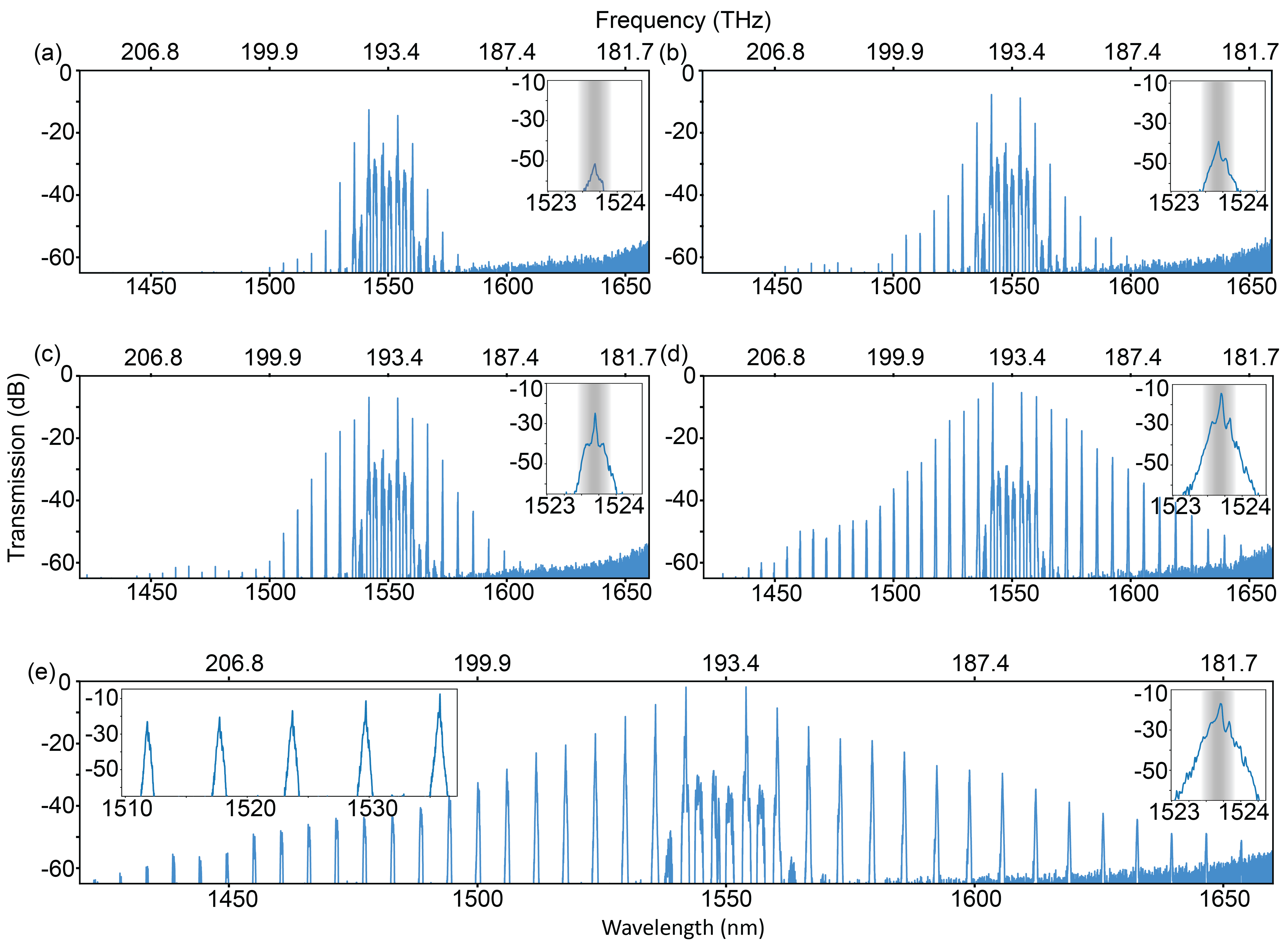
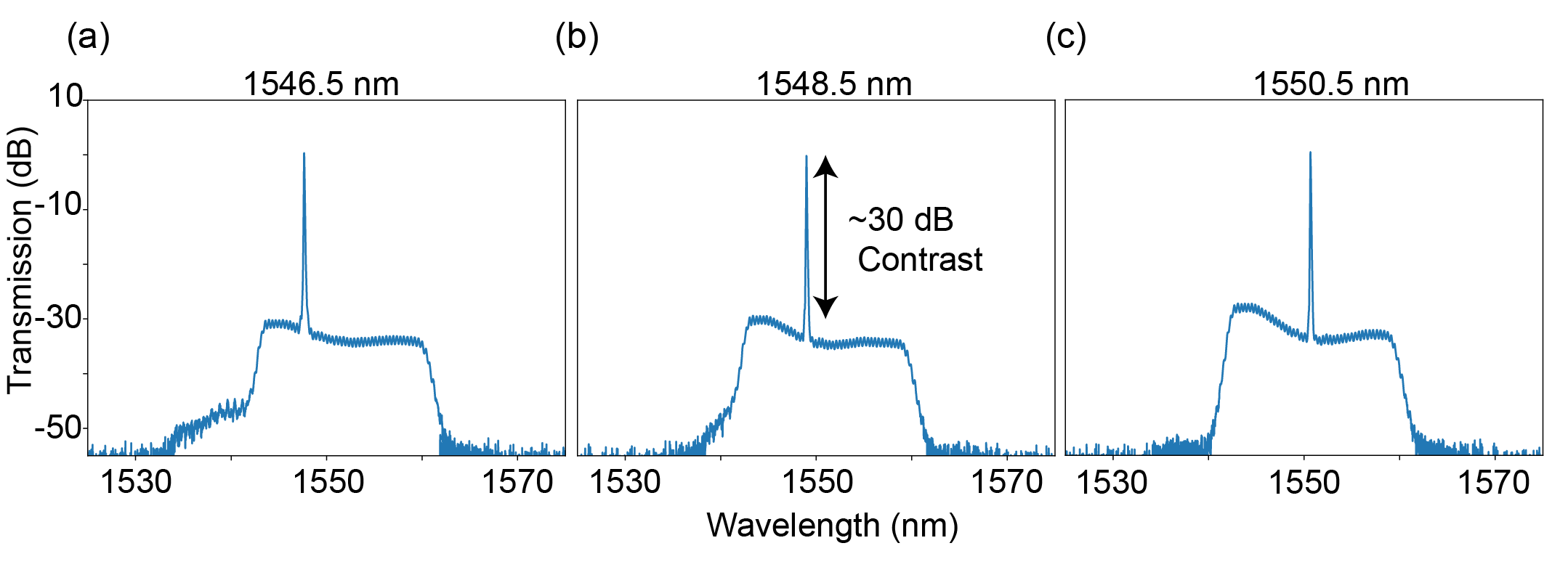
Three pump laser spectra are shown in Figure S5 for three different central wavelengths. As can be seen, the laser background remains approximately 30 dB suppressed from the laser peak regardless of the pump central wavelength.
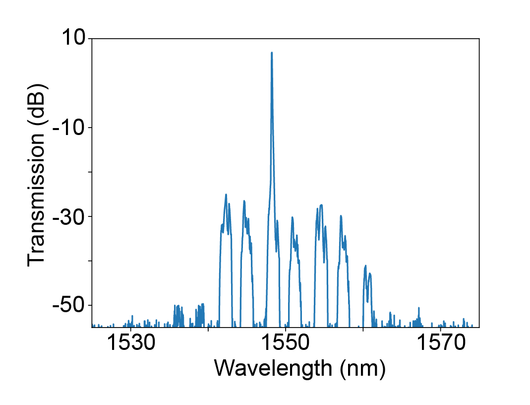
The same laser envelope can be observed when sending the pump through a topological lattice and collecting the drop port spectrum. The output spectrum of an identical AQH lattice as the one used in the nonlinear measurements in this work with a pump power below the comb formation threshold is shown in Figure S6. The broad laser background is transmitted through several edge bands as well as link-ring bands, producing a characteristic structure that can be observed in the main text.
VIII.5 Generation and Spectra of Imaged Modes
For the CCW and CW topological frequency comb images in Figure 4, the peak pump power in the waveguide was approximately 92 W and 100 W respectively. The wavelength was tuned through the edge band to a value of 1547.97 nm. In order to generate a bulk comb, the peak pump power in the waveguide was approximately 125 W and the laser was tuned onto resonance with a bulk mode at 1547.43 nm. Through port spectra of each of these combs are displayed in Figure S7. We note that while the pump power used here for the bulk mode is significantly higher than that of the topological combs, a broader systematic study would be required to determine the minimum power required to generate frequency combs in bulk modes of the lattice. Due to the highly variable nature of these bulk modes, such a study is outside the scope of the present work.