Nano-optical investigation of grain boundaries, strain and edges in CVD grown MoS2 monolayers
Abstract
The role of defects in two-dimensional semiconductors and how they affect the intrinsic properties of these materials have been a wide researched topic over the past decades. Optical characterization such as photoluminescence and Raman spectroscopies are important tools to probe their physical properties and the impact of defects. However, conventional optical techniques present a spatial resolution limitation lying in a m-scale, which can be overcomed by the use of near-field optical measurements. Here, we use tip-enhanced photoluminescence and Raman spectroscopies to unveil nanoscale optical heterogeneities at grain boundaries, local strain fields and edges in grown MoS2 monolayers. A noticeable enhancement of the exciton peak intensity corresponding to a trion emission quenching is observed at narrow regions down to 47 nm of width at grain boundaries related to doping effects. Besides, localized strain fields inside the sample lead to non-uniformities in the intensity and energy position of photoluminescence peaks. Finally, distinct samples present different nano-optical responses at their edges due to strain and passivation defects. The passivated defective edges show a photoluminescence intensity enhancement and energy blueshift as well as a frequency blueshift of the 2LA Raman mode. On the other hand, the strained edges display a photoluminescence energy redshift and frequency redshifts for E2g and 2LA Raman modes. Our work shows that different defect features can be only probed by using optical spectroscopies with a nanometric resolution, thus revealing hindered local impact of different nanoscale defects in two-dimensional materials.
keywords:
American Chemical Society, LaTeXIR,NMR,UV
Two-dimensional transition metal dichalcogenides (TMD) are semiconducting van der Waals materials with remarkable optical and electronic properties such as a transition from an indirect to a direct band gap when thinned to a monolayer 1, 2, strong many-body effects 3, 4, 5, 6, 7 and circular polarized light with valley selectively 8, 9, 10, 11. These properties lead TMDs as potential materials for the next generation of opto-electronic devices 12, 13, 14. However, the grown TMD samples with the large-area required for industrial-scale applications commonly present defects as vacancies, strain fields, electrical and chemical doping, grain boundaries and surface adsorbents 15. These defects are related with optical and electronic properties modifications, which can deeply affect the TMD performance in devices 16. On the other hand, there is also a great effort in the defect engineering of these 2D TMDs in order to achieve novel desirable properties 15, 17. Therefore, the characterization of these defects in TMDs is essential to both help in the development of their growth methods as well as to study the intentionally tuning of their properties.
These defects can be well ascertained with a nanoscale spatial resolution by scanning microscopy measurements such as scanning probe microscopy (SPM), scanning tunneling microscopy (STM) and scanning transmission electron microscopy (STEM) 18, 19, 20, 21. However, to investigate the role of these defects in the inhomogeneity of the optical properties throughout the grown samples there is a spatial resolution limitation of hundreds of nanometers due to the diffraction limit of light. Therefore, confocal optical techniques as -photoluminescence (PL) and -Raman spectroscopy are only able to provide averaged electronic and vibrational responses over a m-scale area. Hence, the precise determination of localized optical modifications by defects cannot be resolved by these techniques. Recently, tip-enhanced PL and Raman spectroscopies (TEPL and TERS, respectively) have also been used to study defective optical features in TMDs 22, 23, 24, 25. As the tip amplifies the light signal due to its plasmonic field, the spatial resolution of these tip-enhanced techniques is determined by the tip size. Thus, investigations of excitonic effects 26, 27, grain boundaries 28, 29, 30, edge defects 31, 32, 33, strain 34, wrinkles 35, 36, lateral interfaces 37, 38, 39, 40, hybrid heterostructures 41 and defect-bound localized states 42, 33 have been carried out by TEPL and TERS measurements. However, due to the implementation challenges of these optical techniques, it is possible to observe that several of these works have not reached the optimal spatial resolution of few dozens of nanometers. Moreover, as defects in grown TMDs can show distinct optical modifications depending on further factors as growth parameters and substrate 43, 44, a wide nanoscale characterization with combined electronic and vibrational information of different defects in TMD grown monolayers is still a demanding task.
In this work we studied several defects in chemical vapor deposition (CVD) grown MoS2 monolayers by TEPL and TERS measurements with spatial resolutions down to nm. We investigated the PL emission along distinct MoS2 monolayers grain boundaries, revealing a remarkable localized intensity enhancement of the exciton peak due to a suppression of trion formation along these defects. Furthermore, non-uniform nanoscale strain fields throughout the sample were also probed by TEPL and TERS measurements. Finally, MoS2 monolayers from distinct set of samples presented different defective edge features. In one case, the MoS2 monolayer displayed an enhanced and blueshifted PL signal at the edges. This PL shift is associated with a frequency shift of cm-1 in the second-order 2LA Raman mode and not at the first order Raman modes, implying in a possible defective electronic state. On the other hand, MoS2 monolayers from the other sample set revealed a distinct response in a nm width region at their edges. A PL redshift is observed at the edges, that corresponds to remarkable frequency redshifts for E2g and 2LA Raman modes. Atomic force microscopy (AFM) measurements were also performed and showed a suspension of nm at the edges, which suggests the presence of a strain field at the MoS2 monolayers edges. Our results highlights the importance of probing both electronic and vibrational responses with nanometer resolution in the 2D materials.
1 Results and discussion
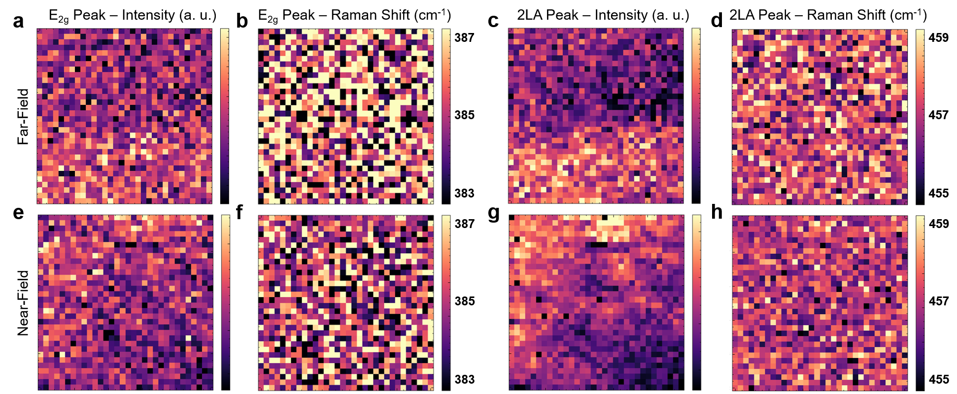
The MoS2 monolayer samples A1 and A2 investigated here were grown by a CVD method in two different batches that led to two different optical characteristics as we will show along the manuscript. Further growth details are described in the Methods Section. We first studied a multi-sided polygonal shaped MoS2 monolayer of A1 sample (see Supporting Information Figure S1a for its optical image). It is well-known that these CVD grown multi-sided TMD monolayers present grains with distinct crystallographic orientations 45, 46. The boundary between the two grains is thus a defective region in which the mismatched atoms present a distinct localized geometrical structure that depends on the relative orientation of the grains. These grain boundaries have been studied for different TMD monolayers in the past years 45, 46, 47, 48, 49, 50, 51. While SPM measurements are capable of determining the nanoscale features of the modified atomic structure along the grain boundaries 45, 46, 47, conventional optical measurements only give the averaged response of m-areas containing these defects 45, 48, 49, 50, 51. Therefore, although intensity enhancements and peak shifts had been reported for TMD monolayers grain boundaries by -PL and -Raman measurements, they were not able to ascertain the area in which the optical properties are affected due to their limited spatial resolution. More recently, TEPL and TERS measurements have also been carried out in monolayer TMDs in order to provide a wider comprehension of the nanoscale character of the grain boundaries optical features 28, 29, 30. However, these few existent reports showed quenched Raman and PL intensities along the grain boundaries, contrary to previously reported features and in accordance with a likely sample damage at these defects. Hence, a careful nano-optical investigation of TMD grain boundaries is required for a deeper understanding of the roles of defects in monolayer TMDs.
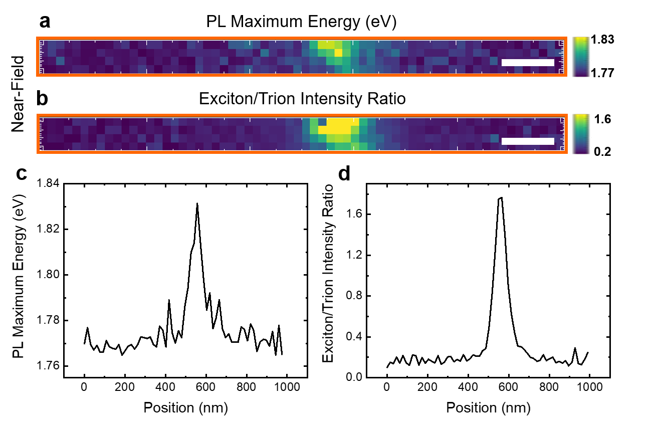
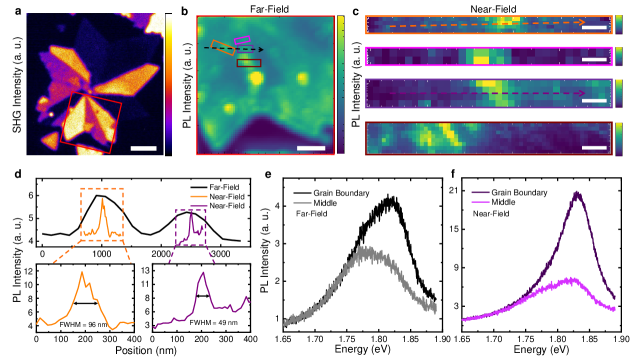
Figure 1a shows a polarized second-harmonic generation (SHG) image of the multi-sided polygonal shaped MoS2 monolayer (see Methods Section for experimental details). Since the SHG in monolayer TMDs is sensitive to the material crystallographic orientation 52, polarized SHG measurements are capable of determining the grain orientations and thus reveals the presence of grain boundaries 53. Hence, the different SHG intensities in Figure 1a shows the distinct grains and their boundaries throughout the MoS2 monolayer. Supporting Information Figure S1c displays the entire polarization dependence of the observed grains and their relative crystallographic orientations. Figure 1b shows the intensity map of a -PL hyperspectral measurement performed in the red squared region displayed in Figure 1a. In agreement with previously reports 45, 49, 50, 51, PL intensity enhancements are observed at grain boundaries. Therefore, in order to ascertain the localization and the real magnitude of the optical modifications in these grain boundaries, we performed TEPL measurements along distinct grain boundaries regions highlighted in colored rectangles in Figure 1b. To show the spatial resolution and signal enhancements of the technique, all TEPL and TERS measurements in this work were carried out with the tip up and down, respective to their far-field (FF) and near-field (NF) responses (further experimental details in Methods Section). Figure 1c displays PL intensity maps of 4 TEPL hyperspectral measurements along MoS2 monolayer grain boundaries regions. The underlined color around each TEPL hyperspectral map is respective to the rectangular areas of the same color in Figure 1b. A localized PL intensity enhancement is noted for all probed grain boundaries. Moreover, an energy blueshift is also observed at the grain boundaries, as shown in Supporting Information Figure S2. To quantify the spatial width of the optical modifications in these defects probed by the NF measurements and compare them with the spatial resolution of the FF measurements, Figure 1d shows PL intensity profiles taken along the black dashed arrow in Figure 1b and orange and purple dashed arrows in Figure 1c. The top intensity profile graph of Figure 1d reveals the remarkable increase in spatial resolution given by the tip. While the grain boundaries in the FF measurement presents spatial widths of nm, the bottom intensity profile graphs unveil that the region affected by these defects can be as narrow as 49 nm. Distinct grain boundaries present different structural modifications, hence it is natural that they also display different affected regions. For instance, the grain boundary presented in the brown underlined TEPL map of Figure 1c shows two separated enhanced lines, that correspond to a broader brighter region in the FF PL map of Figure 1b. Figures 1e,f compare the FF and NF PL spectra, respectively, of grain boundary and grain middle regions. The FF spectra present a PL energy blueshift and an intensity enhancement at the grain boundary. However, these features are emphasized in the NF spectra, which gives the real magnitude of the spectral modifications. As shown in Figure 1f, it can be observed that the grain middle region present a PL spectrum composed by trion and exciton peaks with similar intensities. At the grain boundary, the exciton peak presents a noticeable enhancement while the trion peak is quenched, which is responsible for the observed PL energy blueshift. The exciton/trion peak intensity ratio map shown in Supporting Information Figure S2 reveals a relative enhancement up to 9 times of the exciton intensity with respect to the trion at the grain boundary. This exciton emission increase due to a suppressed trion formation was previously associated to an electrical doping effect 54, which can be locally probed by these near-field measurements 55, 56. In fact, a commonly reported feature at MoS2 monolayer grain boundaries is the presence of electrical doping effects at these regions 45, 57, 50, related with defects such as sulfur vacancies 57 or chemical doping 50. Thus, our results shed light in the nanoscale aspect of the electrical and optical properties modifications of the mismatched grain boundary regions.
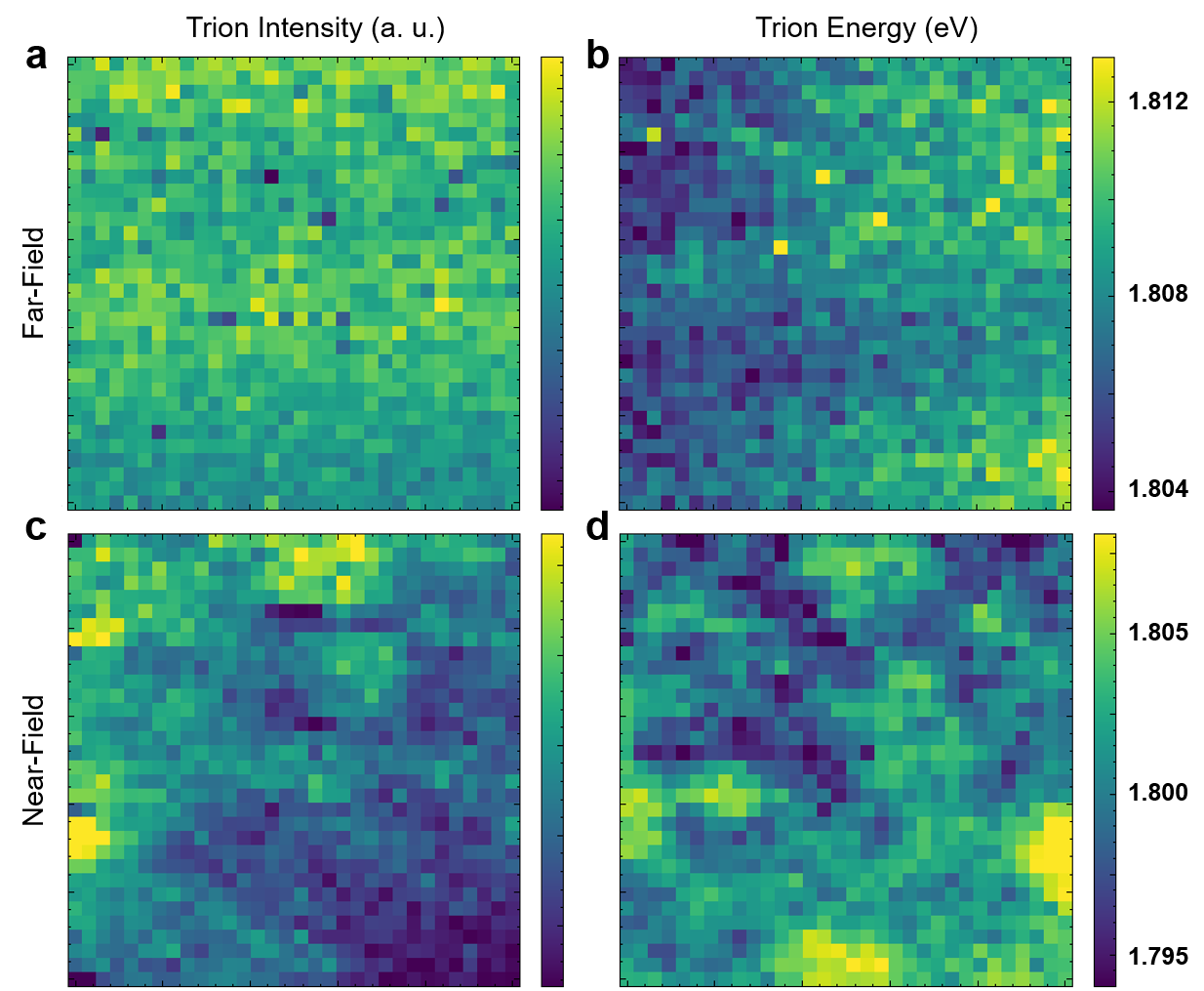
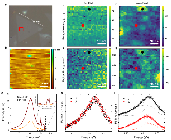
In the following, we performed TEPL and TERS measurements in the A2 sample in order to study further local heterogeneities. Figure 2a shows the optical image of a triangular shaped MoS2 monolayer from the A2 sample. The topography of the x nm squared region in the center of the monolayer highlighted in red in Figure 2a was probed by a non-contact mode AFM measurement (further details in Methods Section), as displayed in Figure 2b showing no large topographical variations along the sample area. Moreover, Figure 2c shows FF and NF spectra with Raman and PL peaks taken in the middle of the MoS2 flake. Spectral enhancement factors of and for PL and Raman intensities, respectively, were observed by engaging the tip. Hyperspectral measurements were also performed in the same region measured by AFM (Figure 2b) to investigate local optical features. The Raman hyperspectrum displayed an uniform response throughout this region in both FF and NF measurements, as shown in Supporting Information Figure S3. However, Figures 2d-g reveal nanoscale modifications in the PL emission over this area. While the FF PL hyperspectrum showed uniform exciton peak intensity (Figure 2d) and energy (Figure 2e) maps, the NF PL hyperspectrum presented local islands of an enhanced exciton intensity (Figure 2f) that matches to an exciton energy blueshift (Figure 2g). To better visualize these features, PL spectra of two distinct positions - p1 (black dot) and p2 (red dot) - are displayed in Figures 2h,i for both FF and NF measurements, respectively. The p1 and p2 position are shown in the PL hyperspectral maps and are related to an enhanced PL signal spot and to a decreased PL signal spot, respectively. Figure 2h presents similar FF PL spectra for p1 and p2, as observed in FF hyperspectral maps. On the other hand, Figure 2i evidences that the NF PL spectra shows an intensity enhancement and energy blueshift at the p1 position. Furthermore, Figure 2i also shows the fitted PL spectra by two Gaussian peaks, respective to the exciton - higher energy peak - and trion - lower energy peak. Supporting Information Figure S4 displays the FF and NF PL maps for the trion emission, presenting a similar behavior with respect to the exciton. It is worth mentioning that all spectra of both FF and NF hyperspectral measurements were fitted by two Gaussian peaks and the hyperspectral maps were made with these fitted parameters.
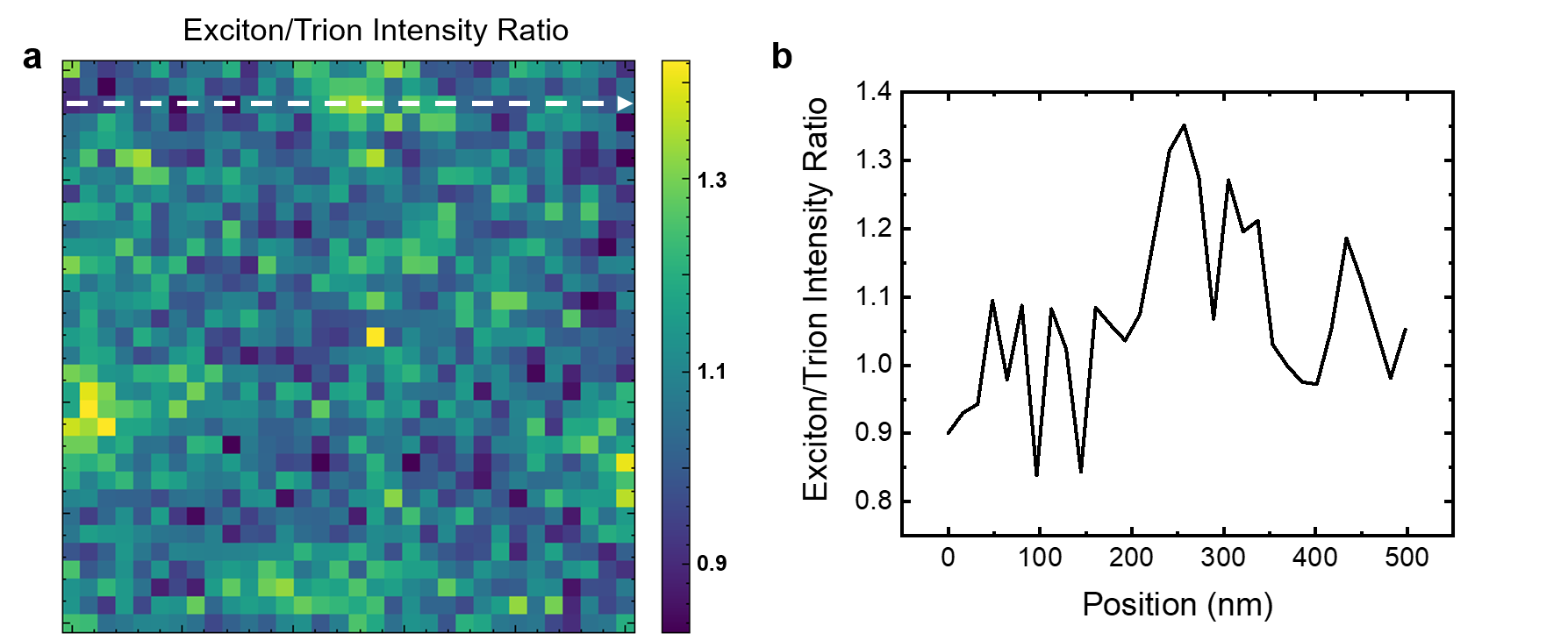
As commented, PL intensity enhancements and energy shifts in MoS2 monolayers can be associated with doping effects. However, as shown in Supporting Information Figure S5, the exciton/trion peak intensity ratio along the measured area is approximately uniform (variations lower than 35%), which is not consistent with a doping hypothesis. Another common feature reported in TMDs that induces PL energy blueshift and intensity enhancement is the variation of strain fields 58, 59, 60, 61 along the sample. CVD grown MoS2 monolayers have previously presented shifts around meV/ of strain for the exciton emission 58, 60. As we observe shifts up to meV for the exciton peak, it would be associated with a strain of . Indeed, this strain is not sufficient to be probed by Raman, as it would induce shifts of cm-1 and cm-1 in the E2g and A1g peaks 60, respectively, that is below our spectrometer resolution. Moreover, the PL intensity enhancement is also in accordance with the strain. Besides, as there is no coincidence between the AFM measurement and the local variation presented in the NF PL maps, the suggestive strain is not accounted on a topographic reason. As shown in Supporting Information Figure S6, this strained regions are also noticed in another region of the flake. Therefore, the observed non-uniform localized strain is presumably due to an expected thermal expansion coefficient and lattice constant mismatch between the monolayer and the substrate 62, which plays a major role in the growth process. Although strain is a well studied characteristic of TMDs, unveiling strained responses at this nanoscale can raise the understanding of the substrate and growth method roles in the optical properties of these 2D semiconductors.
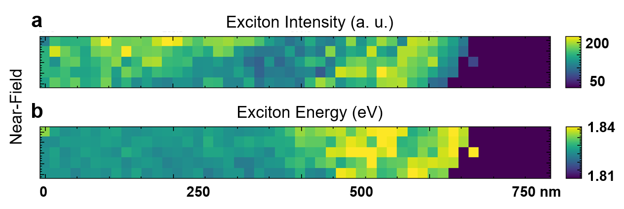
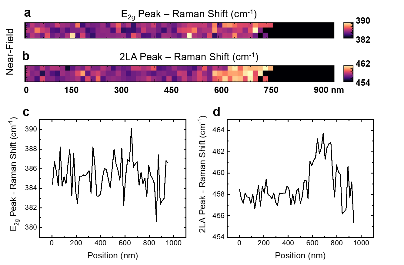
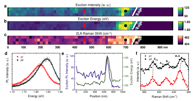
Another frequent heterogeneity reported in monolayer TMDs is associated to their edges 15. Thereby, we have also performed TEPL and TERS hyperspectral measurements in an edge region of the same MoS2 flake shown in Figure 2. Figures 3a,b display the exciton peak intensity and energy maps for the NF PL hyperspectral measurement in this edge region. An intensity enhancement and an energy blueshift of the exciton peak are noted at the edge within a spatial width of less than 100 nm, which was not observed in the FF measurements as shown in Supporting Information Figure S7. These features are also presented in Figure 3d, in which the PL spectra taken at the middle (p1) and at the edge (p2) of the sample confirm the intensity enhancement and energy shift at the edge. Moreover, Supporting Information Figure S8 also shows similar results for another edge region of the same sample. Unlike the PL energy shift in the inferred strained regions throughout the monolayer (Fig. 2), the observed energy shift at the edges are remarkably larger. As can be noticed in the exciton energy profile in Figure 3e, there is an energy shift of meV at the edge. Moreover, this blueshift corresponds to a PL enhancement of , as can also be seen in Figure 3d. If this observed PL energy shift was also due to strain, it would be associated with measurable Raman shifts. However, a NF Raman hyperspectral measurement showed no significant shift for the E2g mode at the edge as shown in Supporting Information Figure S9. On the other hand, the 2LA Raman mode presented a noticeable blueshift of cm-1 as displayed in the TERS peak position map (Figure 3c) and its profile along the edge (Supporting Information Figure S9). The absence of frequency shifts of the first order Raman modes as well as the blueshift of the 2LA mode is also shown in the Raman spectra of the middle p1 position and at the edge p2 position shown in Figure 3f. As shown by Carvalho et al. 63, the MoS2 monolayer 2LA Raman mode is in fact composed by different Raman peaks that are highly dependent with electronic resonances. As these peaks present distinct resonances by varying the laser wavelength 63, a similar behavior is expected if the material band gap is modified. Therefore, the observed 2LA frequency shift at the edge is presumably related to a modification in the relative intensities of the 2LA peaks due to the band gap shift noticed in the PL measurements. Previous reports 64, 65, 66, 31 have observed different PL features at MoS2 monolayer edges due to distinct defects. Water and oxygen passivation of vacancies at the edges also result in an enhancement in the PL intensity, but it corresponds to a redshift in the PL energy 64, 66. On the other hand, a similar nanoscale edge response was recently probed by hyperspectral TEPL measurements 31. However, an assertive determination of the defect responsible for these optical modifications at the edges is still lacking. Therefore, the association of this local PL enhancement and blueshift at the edges with a frequency shift of the 2LA mode brings more information of the influence of the edge defective states in the MoS2 monolayer optical properties.
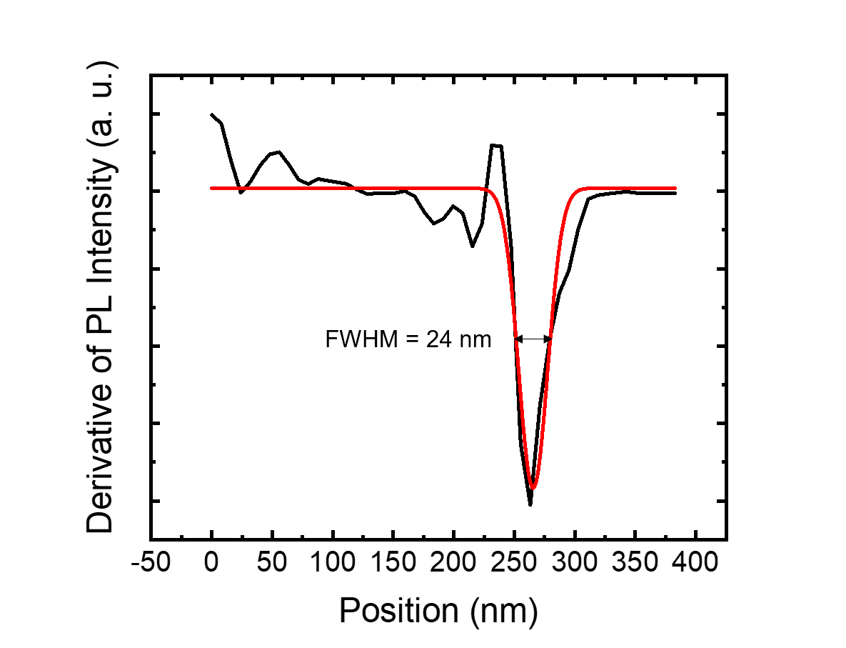
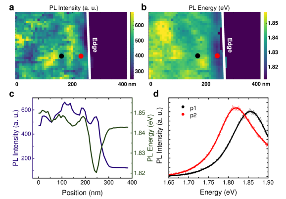
In order to further investigate other types of optical responses at the edges, we have measured other MoS2 monolayer edges from the A1 sample. Figures 4a,b shows the measured NF PL hyperspectrum of a A1 MoS2 monolayer edge. Conversely to the observed features of sample A2, the PL intensity map of Figure 4a presents no clear modification, whereas the PL energy map of Figure 4b reveals a significant redshift in an edge region of less than nm of width. TEPL measurements in distinct edge regions of different monolayer flakes of the same A1 sample presented a similar PL energy redshift, as displayed in Supporting Information Figure S10. Figure 4c shows PL intensity and energy profiles along the edge, in which the energy redshift of meV can be observed. Moreover, in the intensity profile is possible to extract the spatial resolution of the measurement, that is around nm (see further details in Supporting Information Figure S11). PL spectra at the middle (p1 position) and at the edge (p2 position) of the sample are shown in Figure 4d, clearly showing the PL redshift presented in the TEPL hiperspectral map and profile, but no clear spectral modification. Although there is a PL energy redshift associated with oxygen and water passivation at the edges 64, 66, the absence of a strong PL intensity enhancement suggests a different reason for this observed edge response. On the other hand, if this intense PL energy modification at the edge is related with strain, a shift in the first order Raman modes should be observed.
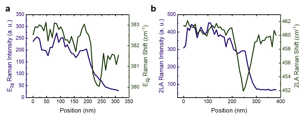
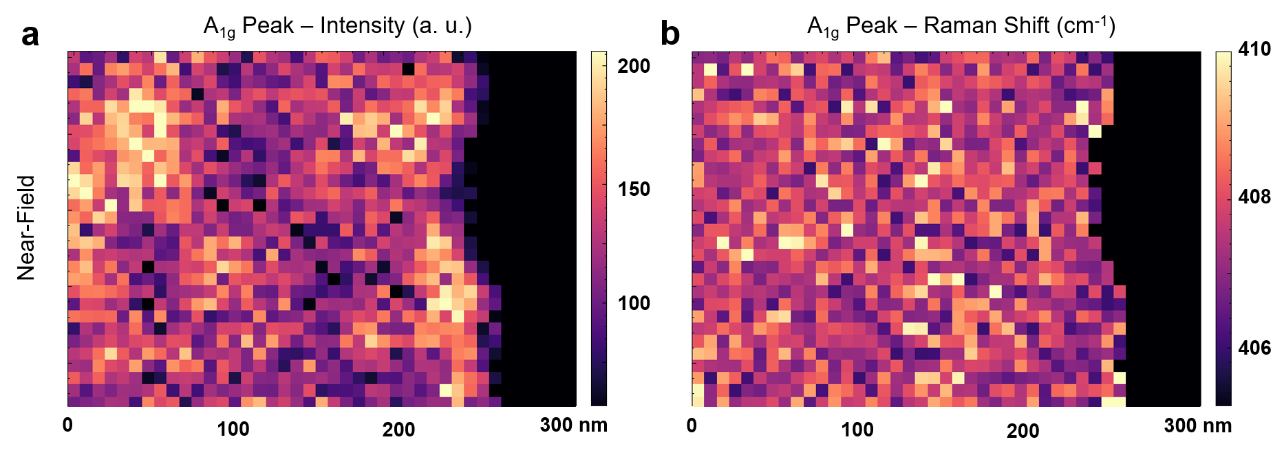
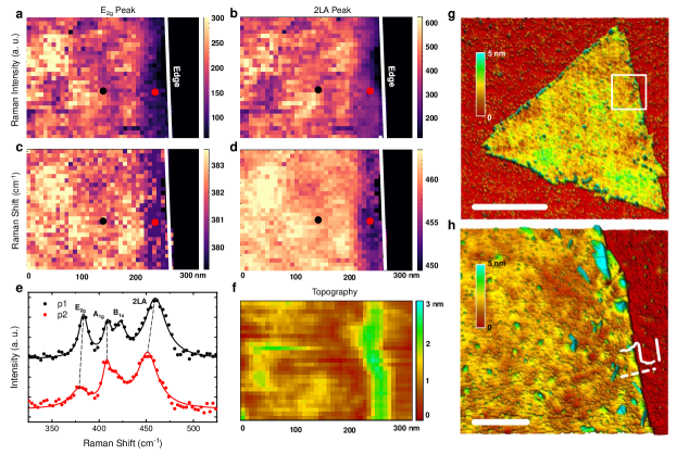
Therefore, we also performed a NF Raman hyperspectral measurement in the same region as the measurements of Figure 4. The Raman intensity maps of the E2g and 2LA modes are displayed in Figures 5a,b, while the frequency maps of these peaks are presented in Figures 5c,d. For both peaks it is observed an intensity quenching and a frequency redshift at the edge. Figure 5e shows Raman spectra taken in the middle of the monolayer (p1) and at its edge (p2), highlighting the features noted in the Raman maps. To better quantify the frequency shifts of the Raman modes, their intensity and frequency profiles along the edge are shown in Supporting Information Figure S12. It can be observed a cm-1 shift at the edge for the E2g peak and a cm-1 for the 2LA mode. As commented for the A2 sample, this 2LA shift can also be associated with the modification in the relative intensities of the 2LA peaks due to their distinct resonant responses 63. Moreover, it is worth commenting that the PL blueshift at the edge of A2 sample related to a 2LA frequency blueshift is in accordance with the PL redshift of the A1 sample at its edge corresponding to a 2LA redshift. Besides, for a strain hypothesis, the cm-1 redshift of the E2g mode is in agreement with the observed PL redshift of meV 60, which would be associated with a strain of approximately . Another commonly reported feature associated with strain with this magnitude in MoS2 monolayer is the splitting of the E2g mode in two peaks due to a lattice symmetry breaking 67. Although we did not have the spectral resolution to resolve these two peaks, the broadening of the E2g mode observed in the Raman spectrum at the edge of Figure 5e is another indication of strain. Furthermore, the Raman intensity and frequency maps and profiles of the A1g mode are shown in Supporting Information Figure S13. Whereas there is an intensity enhancement at the edge, no substantial shift is noted for the A1g peak. The expected A1g shift for a strain is cm-1, which was probably not detected due to our measurement spectral resolution and its convolution with the B1u mode.
In order to further corroborate the strain field responsible for the nanoscale optical features at the edge we performed AFM measurements in the A1 sample to probe possible topographic disorders. Simultaneously with the acquisition of the TEPL and TERS measurements, the topographic response of the tip (non-contact mode AFM) was also measured as shown in Figure 5f. A noticeable suspension in the edge region of less than nm of width can be observed, indicating the presence of a strain field there. In order to confirm this result, high resolution AFM images was measured as displayed in Figures 5g,h. Figure 5g present the AFM for the whole monolayer flake, while Figure 5h shows the AFM for the edge region highlighted in the inset white square of Figure 5g. Besides the surface roughness across the monolayer, both measurements presented a distinct topographic response at the edge, underlined by the height profile in the inset of Figure 5h. Thus, the sample indeed shows a localized topographic variation at the edges that can generate the observed strain fields that could be only probed by NF PL and Raman measurements.
In summary, we studied local defects in distinct CVD grown MoS2 monolayers by NF optical measurements. Electronic structure modifications in nanoscale regions along MoS2 monolayer grain boundaries were probed by TEPL, in which a remarkable intensity enhancement of the exciton peak related to a quenching in the trion peak emission due to a doping effect was revealed. Besides, local strain fields were observed throughout a MoS2 monolayer by TEPL and TERS measurements, revealing the role of the lattice mismatch between sample and substrate. Finally, edge defects were investigated by TEPL and TERS in MoS2 monolayers. While one of the grown MoS2 monolayer presented an PL intensity enhancement and energy blueshift at the edges, the other grown sample showed a PL energy redshift in the edge regions. Moreover, this last sample displayed a frequency redshift in the E2g and 2LA Raman modes as well as a topographic suspension revealed by the AFM measurement, which suggest a strong localized strain field at the edges. Our work highlights the importance of utilizing optical spectroscopies with nanometric resolution to probe localized defects and reveal the optical properties in two-dimensional materials, that would be otherwise hindered in typical micrometer resolved spectroscopies.
2 Methods
2.1 Sample Preparation
Monolayers A1 and A2 of MoS2 were synthesized on fused silica substrates using the CVD technique. Two different single-zone quartz tube furnaces were employed for the growth process, utilizing MoO3 ( purity, Aldrich) and sulfur powder (Aldrich, ) as precursors. Substrates were subjected to ultrasonic cleaning in baths of acetone and isopropyl alcohol for 10 minutes each.
For A1, the monolayer was grown at atmospheric pressure inside a 1-inch diameter quartz tube. The cleaned substrate was positioned over a crucible containing 1.1 mg of MoO3, centered in the tube coinciding with the position of the central thermopar. Another crucible, situated approximately 17 cm upstream from the substrate, held 234 mg of sulfur powder. Ar gas purging was carried out for 20 minutes at a flow rate of 180 standard cubic centimeters per minute (sccm), and during the growth process, a 40 sccm Ar gas flow served as the carrier. The sample temperature underwent an initial ramp to 300 °C at a rate of 7.5 °C.min-1, followed by a second ramp from 300 to 850 °C at a rate of 15 °C.min-1, with a 5-minute hold at the final temperature. At a central temperature of 600 °C, sulfur vapor was introduced by ramping up the temperature of the thermal rubber band at a rate of 50 °C.min-1 until reaching 150 °C, a temperature maintained throughout the growth until complete sulfur evaporation. Following growth, the furnace was powered off and allowed to cool naturally.
For A2, the monolayer was grown under atmospheric pressure inside a 2.5-inch diameter quartz tube. In this case, the cleaned fused silica substrate was placed over a cleaned Si/SiO2 (300nm) substrate. The stacked substrates were positioned over a crucible containing 1.1 mg of MoO3, centered in the tube coinciding with the central thermopar. Another crucible, situated approximately 21 cm upstream from the substrate, held 350 mg of sulfur powder. Ar gas purging and carrier gas conditions were identical to those of A1. The sample temperature underwent an initial ramp to 300 °C at a rate of 7.5 °C.min-1, followed by a second ramp from 300 to 800 °C at a rate of 15 °C.min-1, with a 15-minute hold at the final temperature. Sulfur vaporization commenced when the central temperature reached 600 °C. Following growth, the furnace was powered off and allowed to cool naturally.
2.2 Optical Measurements
In our TERS and TEPL measurements, we employed the FabNS Porto-SNOM system, utilizing an oil-immersion objective lens (NA=1.4), in conjunction with a radially polarized HeNe laser (632.8 nm). The probe tips utilized were the Plasmon-Tunable Tip Pyramid (PTTP) 68, tuned to match the laser wavelength. The acquired spectral data were subsequently analyzed with the PortoFlow Analysis Software (v1.15).
The SHG measurements were carried out by using a picosecond OPO laser (APE Picoemerald), with an incident power of 50 mW at the sample and a 810 nm excitation wavelength. The SHG imaging was performed by scanning the laser with a set of galvanometric mirrors (LaVison BioTec) in a Nikon microscope. The laser beam was focused on the sample by a 40x objective with numerical aperture N.A. = 0.95 after a half-wave plate and the backscattered signal was collected by the same objective and directed to a photomultiplier tube (PMT). We placed an analyzer in front of the PMT that we rotated together with the half-wave plate, as well as a 405/10 nm band-pass filter to collect only the SHG signal. The SHG images were taken in steps of 2° of the half wave plate and analyzer.
2.3 AFM Measurements
High resolution AFM experiments were carried out using a XE-70 atomic force microscope from Park Systems, Korea. All images were acquired in the intermittent contact mode and in ambient conditions. Si cantilevers (DPE/XSC11 hard, from MikroMasch), with spring constants of 3-16 N.m-1 and a tip radius of curvature 10 nm, were used throughout the study for sample imaging. These AFM images were processed (leveling, profiling, and 3D rendering) using the open-source software package Gwyddion.
The topographic response of the tip on the TERS and TEPL measurements were done by a shear force detection feedback AFM (non-contact mode).
The authors acknowledge financial support from CNPq, CAPES, FAPEMIG, FINEP, Brazilian Institute of Science and Technology (INCT) in Carbon Nanomaterials and Rede Mineira de Materiais 2D (FAPEMIG).
Polarized SHG. Exciton/trion intensity ratio maps. Far-field and near-field Raman maps. Far-field and near-field trion maps. Far-field and near-field exciton maps. Near-field spatial resolution. Near-field Raman modes intensity and frequency profiles.
References
- Mak et al. 2010 Mak, K. F.; Lee, C.; Hone, J.; Shan, J.; Heinz, T. F. Atomically Thin : A New Direct-Gap Semiconductor. Physical Review Letters 2010, 105, 136805
- Splendiani et al. 2010 Splendiani, A.; Sun, L.; Zhang, Y.; Li, T.; Kim, J.; Chim, C.-Y.; Galli, G.; Wang, F. Emerging Photoluminescence in Monolayer MoS2. Nano Letters 2010, 10, 1271–1275
- Mak et al. 2013 Mak, K. F.; He, K.; Lee, C.; Lee, G. H.; Hone, J.; Heinz, T. F.; Shan, J. Tightly bound trions in monolayer MoS2. Nature Materials 2013, 12, 207–211
- Chernikov et al. 2014 Chernikov, A.; Berkelbach, T. C.; Hill, H. M.; Rigosi, A.; Li, Y.; Aslan, O. B.; Reichman, D. R.; Hybertsen, M. S.; Heinz, T. F. Exciton Binding Energy and Nonhydrogenic Rydberg Series in Monolayer . Physical Review Letters 2014, 113, 76802
- Ugeda et al. 2014 Ugeda, M. M.; Bradley, A. J.; Shi, S.-F.; da Jornada, F. H.; Zhang, Y.; Qiu, D. Y.; Ruan, W.; Mo, S.-K.; Hussain, Z.; Shen, Z.-X.; Wang, F.; Louie, S. G.; Crommie, M. F. Giant bandgap renormalization and excitonic effects in a monolayer transition metal dichalcogenide semiconductor. Nature Materials 2014, 13, 1091–1095
- He et al. 2014 He, K.; Kumar, N.; Zhao, L.; Wang, Z.; Mak, K. F.; Zhao, H.; Shan, J. Tightly Bound Excitons in Monolayer . Physical Review Letters 2014, 113, 26803
- Sousa et al. 2023 Sousa, F. B.; Perea-Causin, R.; Hartmann, S.; Lafetá, L.; Rosa, B.; Brem, S.; Palekar, C.; Reitzenstein, S.; Hartschuh, A.; Malic, E.; Malard, L. M. Ultrafast hot electron–hole plasma photoluminescence in two-dimensional semiconductors. Nanoscale 2023, –
- Xiao et al. 2012 Xiao, D.; Liu, G.-B.; Feng, W.; Xu, X.; Yao, W. Coupled Spin and Valley Physics in Monolayers of and Other Group-VI Dichalcogenides. Physical Review Letters 2012, 108, 196802
- Mak et al. 2012 Mak, K. F.; He, K.; Shan, J.; Heinz, T. F. Control of valley polarization in monolayer MoS2 by optical helicity. Nature Nanotechnology 2012, 7, 494–498
- Zeng et al. 2012 Zeng, H.; Dai, J.; Yao, W.; Xiao, D.; Cui, X. Valley polarization in MoS2 monolayers by optical pumping. Nature Nanotechnology 2012, 7, 490–493
- Cao et al. 2012 Cao, T.; Wang, G.; Han, W.; Ye, H.; Zhu, C.; Shi, J.; Niu, Q.; Tan, P.; Wang, E.; Liu, B.; Feng, J. Valley-selective circular dichroism of monolayer molybdenum disulphide. Nature Communications 2012, 3, 887
- Radisavljevic et al. 2011 Radisavljevic, B.; Radenovic, A.; Brivio, J.; Giacometti, V.; Kis, A. Single-layer MoS2 transistors. Nature Nanotechnology 2011, 6, 147–150
- Lopez-Sanchez et al. 2013 Lopez-Sanchez, O.; Lembke, D.; Kayci, M.; Radenovic, A.; Kis, A. Ultrasensitive photodetectors based on monolayer MoS2. Nature Nanotechnology 2013, 8, 497–501
- Pospischil et al. 2014 Pospischil, A.; Furchi, M. M.; Mueller, T. Solar-energy conversion and light emission in an atomic monolayer p–n diode. Nature Nanotechnology 2014, 9, 257–261
- Lin et al. 2016 Lin, Z.; Carvalho, B. R.; Kahn, E.; Lv, R.; Rao, R.; Terrones, H.; Pimenta, M. A.; Terrones, M. Defect engineering of two-dimensional transition metal dichalcogenides. 2D Materials 2016, 3, 22002
- Zhang et al. 2019 Zhang, Y.; Yao, Y.; Sendeku, M. G.; Yin, L.; Zhan, X.; Wang, F.; Wang, Z.; He, J. Recent Progress in CVD Growth of 2D Transition Metal Dichalcogenides and Related Heterostructures. Advanced Materials 2019, 31, 1901694
- Liang et al. 2021 Liang, Q.; Zhang, Q.; Zhao, X.; Liu, M.; Wee, A. T. S. Defect Engineering of Two-Dimensional Transition-Metal Dichalcogenides: Applications, Challenges, and Opportunities. ACS Nano 2021, 15, 2165–2181
- Addou et al. 2015 Addou, R.; Colombo, L.; Wallace, R. M. Surface Defects on Natural MoS2. ACS Applied Materials & Interfaces 2015, 7, 11921–11929
- Prado et al. 2015 Prado, M. C.; Nascimento, R.; Faria, B. E. N.; Matos, M. J. S.; Chacham, H.; Neves, B. R. A. Nanometre-scale identification of grain boundaries in MoS2 through molecular decoration. Nanotechnology 2015, 26, 475702
- Fei et al. 2016 Fei, L.; Lei, S.; Zhang, W.-B.; Lu, W.; Lin, Z.; Lam, C. H.; Chai, Y.; Wang, Y. Direct TEM observations of growth mechanisms of two-dimensional MoS2 flakes. Nature Communications 2016, 7, 12206
- Wang et al. 2018 Wang, S.; Robertson, A.; Warner, J. H. Atomic structure of defects and dopants in 2D layered transition metal dichalcogenides. Chemical Society Reviews 2018, 47, 6764–6794
- Malard et al. 2021 Malard, L. M.; Lafeta, L.; Cunha, R. S.; Nadas, R.; Gadelha, A.; Cançado, L. G.; Jorio, A. Studying 2D materials with advanced Raman spectroscopy: CARS, SRS and TERS. Physical Chemistry Chemical Physics 2021, 23, 23428–23444
- Kim and Kim 2021 Kim, Y.; Kim, J. Near-field optical imaging and spectroscopy of 2D-TMDs. Nanophotonics 2021, 10, 3397–3415
- Shao and Su 2022 Shao, J.; Su, W. Tip-enhanced nanoscopy of two-dimensional transition metal dichalcogenides: progress and perspectives. Nanoscale 2022, 14, 17119–17133
- Kwon et al. 2023 Kwon, S.; Kim, J. M.; Ma, P. J.; Guan, W.; Nam, S. Near-Field Nano-Optical Imaging of van der Waals Materials. Advanced Physics Research 2023, n/a, 2300009
- Su et al. 2016 Su, W.; Kumar, N.; Mignuzzi, S.; Crain, J.; Roy, D. Nanoscale mapping of excitonic processes in single-layer MoS2 using tip-enhanced photoluminescence microscopy. Nanoscale 2016, 8, 10564–10569
- Okuno et al. 2018 Okuno, Y.; Lancry, O.; Tempez, A.; Cairone, C.; Bosi, M.; Fabbri, F.; Chaigneau, M. Probing the nanoscale light emission properties of a CVD-grown MoS2 monolayer by tip-enhanced photoluminescence. Nanoscale 2018, 10, 14055–14059
- Lee et al. 2015 Lee, Y.; Park, S.; Kim, H.; Han, G. H.; Lee, Y. H.; Kim, J. Characterization of the structural defects in CVD-grown monolayered MoS2 using near-field photoluminescence imaging. Nanoscale 2015, 7, 11909–11914
- Smithe et al. 2018 Smithe, K. K. H.; Krayev, A. V.; Bailey, C. S.; Lee, H. R.; Yalon, E.; Aslan, B.; Muñoz Rojo, M.; Krylyuk, S.; Taheri, P.; Davydov, A. V.; Heinz, T. F.; Pop, E. Nanoscale Heterogeneities in Monolayer MoSe2 Revealed by Correlated Scanning Probe Microscopy and Tip-Enhanced Raman Spectroscopy. ACS Applied Nano Materials 2018, 1, 572–579
- Su et al. 2021 Su, W.; Kumar, N.; Shu, H.; Lancry, O.; Chaigneau, M. In Situ Visualization of Optoelectronic Behavior of Grain Boundaries in Monolayer WSe2 at the Nanoscale. The Journal of Physical Chemistry C 2021, 125, 26883–26891
- Rodriguez et al. 2019 Rodriguez, A.; Verhagen, T.; Kalbac, M.; Vejpravova, J.; Frank, O. Imaging Nanoscale Inhomogeneities and Edge Delamination in As-Grown MoS2 Using Tip-Enhanced Photoluminescence. physica status solidi (RRL) – Rapid Research Letters 2019, 13, 1900381
- Huang et al. 2019 Huang, T.-X.; Cong, X.; Wu, S.-S.; Lin, K.-Q.; Yao, X.; He, Y.-H.; Wu, J.-B.; Bao, Y.-F.; Huang, S.-C.; Wang, X.; Tan, P.-H.; Ren, B. Probing the edge-related properties of atomically thin MoS2 at nanoscale. Nature Communications 2019, 10, 5544
- Wang et al. 2023 Wang, J.; Han, Z.; He, Z.; Wang, K.; Liu, X.; Sokolov, A. V. Tip-enhanced photoluminescence of monolayer MoS2 increased and spectrally shifted by injection of electrons. Nanophotonics 2023, 12, 2937–2943
- Rahaman et al. 2017 Rahaman, M.; Rodriguez, R. D.; Plechinger, G.; Moras, S.; Schüller, C.; Korn, T.; Zahn, D. R. T. Highly Localized Strain in a MoS2/Au Heterostructure Revealed by Tip-Enhanced Raman Spectroscopy. Nano Letters 2017, 17, 6027–6033
- Kato et al. 2019 Kato, R.; Umakoshi, T.; Sam, R. T.; Verma, P. Probing nanoscale defects and wrinkles in MoS2 by tip-enhanced Raman spectroscopic imaging. Applied Physics Letters 2019, 114, 73105
- Shao et al. 2022 Shao, J.; Chen, F.; Su, W.; Kumar, N.; Zeng, Y.; Wu, L.; Lu, H.-W. Probing Nanoscale Exciton Funneling at Wrinkles of Twisted Bilayer MoS2 Using Tip-Enhanced Photoluminescence Microscopy. The Journal of Physical Chemistry Letters 2022, 13, 3304–3309
- Sahoo et al. 2019 Sahoo, P. K.; Zong, H.; Liu, J.; Xue, W.; Lai, X.; Gutiérrez, H. R.; Voronine, D. V. Probing nano-heterogeneity and aging effects in lateral 2D heterostructures using tip-enhanced photoluminescence. Optical Materials Express 2019, 9, 1620–1631
- Shao et al. 2021 Shao, J.; Chen, F.; Su, W.; Zeng, Y.; Lu, H.-W. Multimodal Nanoscopic Study of Atomic Diffusion and Related Localized Optoelectronic Response of WS2/MoS2 Lateral Heterojunctions. ACS Applied Materials & Interfaces 2021, 13, 20361–20370
- Fali et al. 2021 Fali, A.; Zhang, T.; Terry, J. P.; Kahn, E.; Fujisawa, K.; Kabius, B.; Koirala, S.; Ghafouri, Y.; Zhou, D.; Song, W.; Yang, L.; Terrones, M.; Abate, Y. Photodegradation Protection in 2D In-Plane Heterostructures Revealed by Hyperspectral Nanoimaging: The Role of Nanointerface 2D Alloys. ACS Nano 2021, 15, 2447–2457
- Garg et al. 2022 Garg, S.; Fix, J. P.; Krayev, A. V.; Flanery, C.; Colgrove, M.; Sulkanen, A. R.; Wang, M.; Liu, G.-Y.; Borys, N. J.; Kung, P. Nanoscale Raman Characterization of a 2D Semiconductor Lateral Heterostructure Interface. ACS Nano 2022, 16, 340–350
- Gadelha et al. 2023 Gadelha, A. C.; Santos, J. C. C.; Rabelo, C.; Vasconcelos, T. L.; Alencar, R. S.; Monken, V.; Miranda, H. L. S.; Cury, L. A.; Jaques, Y. M.; Tromer, R. M.; Galvão, D. S.; Cançado, L. G.; Neves, B. R. A.; Jorio, A. Locally-enhanced optical properties in a hybrid organic/inorganic (coronene/MoS2) Van der Waals heterostructure. 2D Materials 2023, 10, 25015
- Lee et al. 2017 Lee, Y.; Yun, S. J.; Kim, Y.; Kim, M. S.; Han, G. H.; Sood, A. K.; Kim, J. Near-field spectral mapping of individual exciton complexes of monolayer WS2 correlated with local defects and charge population. Nanoscale 2017, 9, 2272–2278
- Buscema et al. 2014 Buscema, M.; Steele, G. A.; van der Zant, H. S. J.; Castellanos-Gomez, A. The effect of the substrate on the Raman and photoluminescence emission of single-layer MoS2. Nano Research 2014, 7, 561–571
- Senkić et al. 2023 Senkić, A.; Bajo, J.; Supina, A.; Radatović, B.; Vujičić, N. Effects of CVD growth parameters on global and local optical properties of MoS2 monolayers. Materials Chemistry and Physics 2023, 296, 127185
- van der Zande et al. 2013 van der Zande, A. M.; Huang, P. Y.; Chenet, D. A.; Berkelbach, T. C.; You, Y.; Lee, G.-H.; Heinz, T. F.; Reichman, D. R.; Muller, D. A.; Hone, J. C. Grains and grain boundaries in highly crystalline monolayer molybdenum disulphide. Nature Materials 2013, 12, 554–561
- Zhou et al. 2013 Zhou, W.; Zou, X.; Najmaei, S.; Liu, Z.; Shi, Y.; Kong, J.; Lou, J.; Ajayan, P. M.; Yakobson, B. I.; Idrobo, J.-C. Intrinsic Structural Defects in Monolayer Molybdenum Disulfide. Nano Letters 2013, 13, 2615–2622
- Azizi et al. 2014 Azizi, A.; Zou, X.; Ercius, P.; Zhang, Z.; Elías, A. L.; Perea-López, N.; Stone, G.; Terrones, M.; Yakobson, B. I.; Alem, N. Dislocation motion and grain boundary migration in two-dimensional tungsten disulphide. Nature Communications 2014, 5, 4867
- Ly et al. 2014 Ly, T. H.; Chiu, M.-H.; Li, M.-Y.; Zhao, J.; Perello, D. J.; Cichocka, M. O.; Oh, H. M.; Chae, S. H.; Jeong, H. Y.; Yao, F.; Li, L.-J.; Lee, Y. H. Observing Grain Boundaries in CVD-Grown Monolayer Transition Metal Dichalcogenides. ACS Nano 2014, 8, 11401–11408
- Kim et al. 2016 Kim, M. S.; Yun, S. J.; Lee, Y.; Seo, C.; Han, G. H.; Kim, K. K.; Lee, Y. H.; Kim, J. Biexciton Emission from Edges and Grain Boundaries of Triangular WS2 Monolayers. ACS Nano 2016, 10, 2399–2405
- Karvonen et al. 2017 Karvonen, L.; Säynätjoki, A.; Huttunen, M. J.; Autere, A.; Amirsolaimani, B.; Li, S.; Norwood, R. A.; Peyghambarian, N.; Lipsanen, H.; Eda, G.; Kieu, K.; Sun, Z. Rapid visualization of grain boundaries in monolayer MoS2 by multiphoton microscopy. Nature Communications 2017, 8, 15714
- Rosa et al. 2022 Rosa, B. L. T.; Fujisawa, K.; Santos, J. C. C.; Zhang, T.; Matos, M. J. S.; Sousa, F. B.; Barbosa, T. C.; Lafeta, L.; Ramos, S. L. L. M.; Carvalho, B. R.; Chacham, H.; Neves, B. R. A.; Terrones, M.; Malard, L. M. Investigation of spatially localized defects in synthetic monolayers. Physical Review B 2022, 106, 115301
- Malard et al. 2013 Malard, L. M.; Alencar, T. V.; Barboza, A. P. M.; Mak, K. F.; de Paula, A. M. Observation of intense second harmonic generation from MoS2 atomic crystals. Physical Review B 2013, 87, 201401
- Yin et al. 2014 Yin, X.; Ye, Z.; Chenet, D. A.; Ye, Y.; O’Brien, K.; Hone, J. C.; Zhang, X. Edge Nonlinear Optics on a MoS¡sub¿2¡/sub¿ Atomic Monolayer. Science 2014, 344, 488 LP – 490
- Mouri et al. 2013 Mouri, S.; Miyauchi, Y.; Matsuda, K. Tunable Photoluminescence of Monolayer MoS2 via Chemical Doping. Nano Letters 2013, 13, 5944–5948
- Gadelha et al. 2021 Gadelha, A. C.; Vasconcelos, T. L.; Cançado, L. G.; Jorio, A. Nano-optical Imaging of In-Plane Homojunctions in Graphene and MoS2 van der Waals Heterostructures on Talc and SiO2. The Journal of Physical Chemistry Letters 2021, 12, 7625–7631
- Nadas et al. 2023 Nadas, R. B.; Gadelha, A. C.; Barbosa, T. C.; Rabelo, C.; de Lourenço e Vasconcelos, T.; Monken, V.; Portes, A. V. R.; Watanabe, K.; Taniguchi, T.; Ramirez, J. C.; Campos, L. C.; Saito, R.; Cançado, L. G.; Jorio, A. Spatially Coherent Tip-Enhanced Raman Spectroscopy Measurements of Electron–Phonon Interaction in a Graphene Device. Nano Letters 2023, 23, 8827–8832
- Bao et al. 2015 Bao, W. et al. Visualizing nanoscale excitonic relaxation properties of disordered edges and grain boundaries in monolayer molybdenum disulfide. Nature Communications 2015, 6, 7993
- Liu et al. 2014 Liu, Z. et al. Strain and structure heterogeneity in MoS2 atomic layers grown by chemical vapour deposition. Nature Communications 2014, 5, 5246
- Castellanos-Gomez et al. 2015 Castellanos-Gomez, A.; Singh, V.; van der Zant, H. S. J.; Steele, G. A. Mechanics of freely-suspended ultrathin layered materials. Annalen der Physik 2015, 527, 27–44
- Christopher et al. 2019 Christopher, J. W.; Vutukuru, M.; Lloyd, D.; Bunch, J. S.; Goldberg, B. B.; Bishop, D. J.; Swan, A. K. Monolayer MoS2 Strained to 1.3Microelectromechanical System. Journal of Microelectromechanical Systems 2019, 28, 254–263
- Li et al. 2020 Li, Z. et al. Efficient strain modulation of 2D materials via polymer encapsulation. Nature Communications 2020, 11, 1151
- Deng et al. 2018 Deng, S.; Sumant, A. V.; Berry, V. Strain engineering in two-dimensional nanomaterials beyond graphene. Nano Today 2018, 22, 14–35
- Carvalho et al. 2017 Carvalho, B. R.; Wang, Y.; Mignuzzi, S.; Roy, D.; Terrones, M.; Fantini, C.; Crespi, V. H.; Malard, L. M.; Pimenta, M. A. Intervalley scattering by acoustic phonons in two-dimensional MoS2 revealed by double-resonance Raman spectroscopy. Nature Communications 2017, 8, 14670
- Birmingham et al. 2018 Birmingham, B.; Yuan, J.; Filez, M.; Fu, D.; Hu, J.; Lou, J.; Scully, M. O.; Weckhuysen, B. M.; Zhang, Z. Spatially-Resolved Photoluminescence of Monolayer MoS2 under Controlled Environment for Ambient Optoelectronic Applications. ACS Applied Nano Materials 2018, 1, 6226–6235
- Kumar et al. 2018 Kumar, P.; Chatterjee, D.; Maeda, T.; Roy, A.; Kaneko, K.; Balakrishnan, V. Scalable faceted voids with luminescent enhanced edges in WS2 monolayers. Nanoscale 2018, 10, 16321–16331
- Hu et al. 2019 Hu, Z.; Avila, J.; Wang, X.; Leong, J. F.; Zhang, Q.; Liu, Y.; Asensio, M. C.; Lu, J.; Carvalho, A.; Sow, C. H.; Castro Neto, A. H. The Role of Oxygen Atoms on Excitons at the Edges of Monolayer WS2. Nano Letters 2019, 19, 4641–4650
- Conley et al. 2013 Conley, H. J.; Wang, B.; Ziegler, J. I.; Haglund, R. F. J.; Pantelides, S. T.; Bolotin, K. I. Bandgap Engineering of Strained Monolayer and Bilayer MoS2. Nano Letters 2013, 13, 3626–3630
- Vasconcelos et al. 2018 Vasconcelos, T. L.; Archanjo, B. S.; Oliveira, B. S.; Valaski, R.; Cordeiro, R. C.; Medeiros, H. G.; Rabelo, C.; Ribeiro, A.; Ercius, P.; Achete, C. A., et al. Plasmon-Tunable Tip Pyramids: Monopole Nanoantennas for Near-Field Scanning Optical Microscopy. Advanced Optical Materials 2018, 6, 1800528
Supporting Information for
Nano-optical investigation of grain boundaries, strain and edges in CVD grown MoS2 monolayers
Frederico B. Sousa, Rafael Battistella Nadas, Rafael Martins, Ana P. M. Barboza, Bernardo R. A. Neves, Ive Silvestre, Ado Jorio, and Leandro M. Malard.
This Supporting Information includes:
Figure S1. Optical image and polarized SHG of MoS2 monolayer sample A1.
Figure S2. PL maximum energy and exciton/trion intensity ratio maps at the grain boundary of MoS2 monolayer sample A1.
Figure S3. Far-field and near-field Raman maps of MoS2 monolayer sample A2.
Figure S4. Far-field and near-field trion maps of MoS2 monolayer sample A2.
Figure S5. Exciton/trion intensity ratio map of MoS2 monolayer sample A2.
Figure S6. Near-field exciton maps of MoS2 monolayer sample A2.
Figure S7. Far-field exciton maps at the edge of MoS2 monolayer sample A2.
Figure S8. Near-field exciton maps at the edge of MoS2 monolayer sample A2.
Figure S9. Near-field Raman maps at the edge of MoS2 monolayer sample A2.
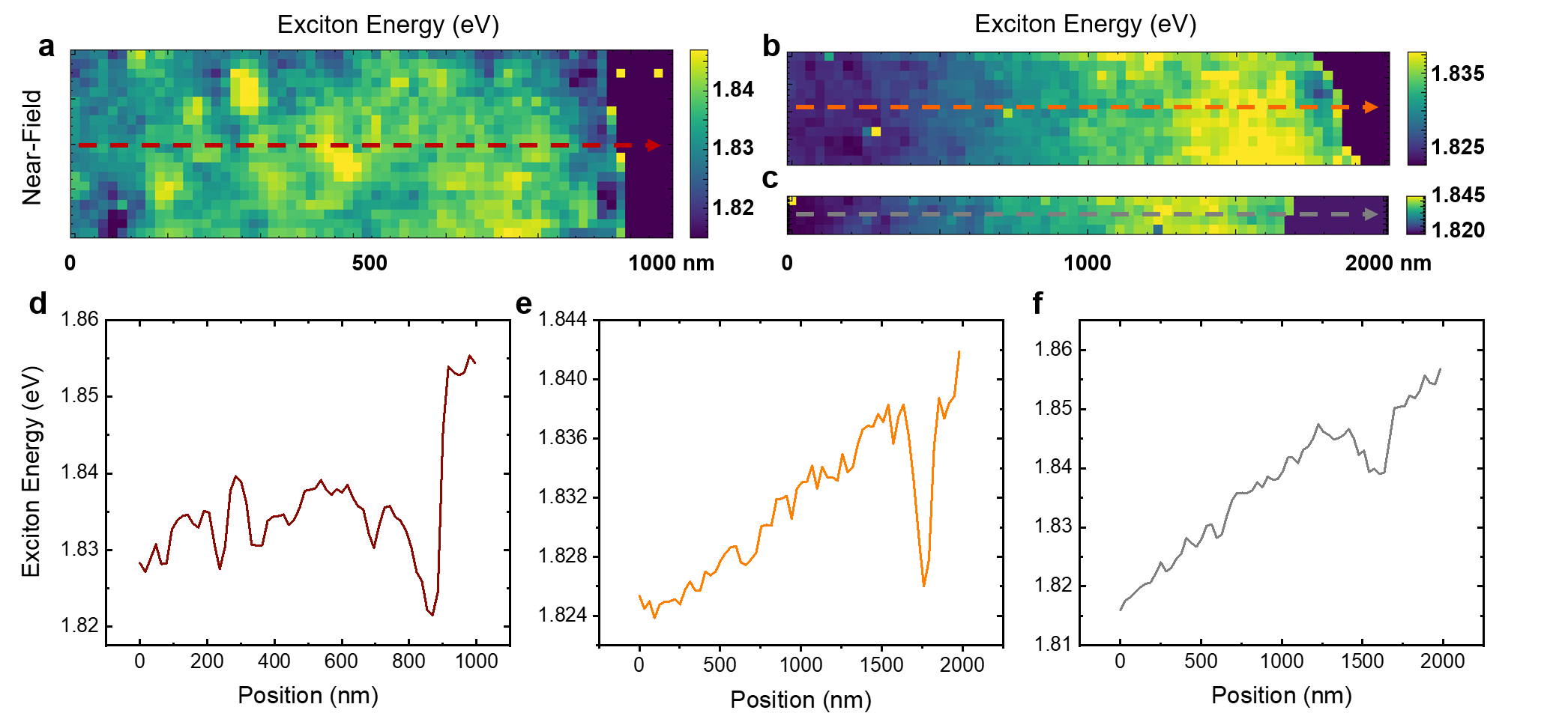
Figure S10. Near-field exciton maps at the edge of MoS2 monolayer sample A1.
Figure S11. Near-field spatial resolution.
Figure S12. Near-field Raman modes intensity and frequency profiles along the edge of MoS2 monolayer sample A1.
Figure S13. Near-field A1g maps at the edge of MoS2 monolayer sample A1.

