Fractal Quantum Transport in \chMoS2 Superlattices
Abstract
We study the band structure and quantum transport of \chMoS2 on a nanometer-scale periodic potential under magnetic fields. Using the continuum model, we compute the band structure of the system with and without magnetic fields. We found the formation of a self-similar fractal band gaps for values of the magnetic field of about . Additionally, we simulate the quantum transport along a realistic two-terminal device affected by the same potential and find a remarkably good consistency between these two apporaches. Our results can be extended to provide a theoretical understanding on the transport phenomenon on transition metal-dichalcogenides.
During the past decade, we have witnessed the rise of transition metal-dichalcogenides, which have become a platform to explore many physical phenomena and phase transitions in two-dimensional (2D) systems, including spin-orbit coupling [1], exciton condensates [2, 3], superconductivity [4, 5, 6] and ferroelectricity [7, 8]. Among this rich family of materials, \chMoS2, a 2D semiconductor with a direct band gap of at the K-point [9, 10], has stood up as a formidable candidate to lead the next generation of electronic devices [11, 12, 13], where gating enables us to control the electron concentration [14] and external electric fields can even induce superconductivity [15]. More recently, with the advent of twistronics [16], engineering stacks of \chMoS2 monolayers with a relative angle between them became a tuning knob that allowed to extend the toolbox of methods for exploring new physics in \chMoS2 heterostructures [8].
On the other hand, applying magnetic fields has also been used to study the properties of \chMoS2 [17, 18]. Typically, weak magnetic fields (–) discretizes the electronic spectrum in a series of Landau levels, which generates distinctive signatures in the quantum transport, such as Shubnikov-de Haas oscillations [19, 20, 21]. At higher values of the magnetic fields, it is expected that the electronic spectrum of \chMoS2 exhibits a fractal self-similar structure of band gaps as a function of magnetic field [22], often referred to as Hofstadter’s butterfly [23]. However, the values of the magnetic field required for its observation are orders of magnitude greater than those achievable in experiments. Superlattice potentials, with nanometer-scale lattice constants, have allowed the observation of the Hofstadter’s spectrum in graphene materials, which have been extensively studied both theoretically [24, 25, 26, 27, 28, 29, 30, 31] and experimentally [32, 33, 34, 35, 36, 37]. However, a similar study on \chMoS2 superlattices is still missing.

In this Letter, we investigate the electronic structure, with and without a perpendicular magnetic field, of a monolayer \chMoS2 under a hexagonal superlattice potential arising from another \chMoS2 layer twisted and stacked on top of it, and the corresponding transport properties, considering a two-terminal device schematically shown in Figure 1(a). In particular, we focus on the energy range close to the conduction and valence band edges, as \chMoS2 hosts a direct band gap at the K-point, where the wavefunction of band edges are mostly prescribed by the d-orbtals of molybdenum [38, 39, 40]. They form a hexagonal lattice with lattice constant , thus here we model the spectrum as a two-dimensional electron gas (2DEG), with effective masses and [39] ( is the free electron mass), in the conduction and valence side, respectively [41]. As sketched in Figure 1(a), the additional \chMoS2 layer, assumed to be uncontacted and serve only as a proximity background layer, makes a twist angle of set to be in this work, resulting in a hexagonal superlattice with periodicity . Note, however, that our results are not limited to any particular , as long as the resulting is on the order of , suitable for experimental observations.
In order to focus on the conduction and valence band edges where the energy bands of \chMoS2 are strictly parabolic, as well as to minimize the complexity of the moiré superlattice potential, the above described system is modeled by the following Hamiltonian:
| (1) |
where is the band index and
| (2) |
is the model potential accounting for the moiré pattern of the twisted bilayer \chMoS2 with the reciprocal superlattice vectors given by with . Note that despite the simplicity of Eq. (2), it was first adopted to describe the superlattice in graphene due to the aligned hexagonal boron nitride (hBN) lattice [42], and later found to give rather satisfactory quantum transport simulations [43, 44].
The parameter in Eq. (2) characterizing the strength of the periodic potential was estimated to be for the graphene/hBN case [42], and here originates from the coupling between d-orbitals of molybdenum atoms in different layers. While this phenomenological parameter is unknown, several ab initio studies suggest that the interlayer between two \chMoS2 monolayers is generally weak [45, 46, 47, 48, 49, 50]. Thus, here we consider a value of and employ the continuum model [51, 52, 53, 54] to construct its band structure. The first term in the Hamiltonian (1) is diagonal in the basis of plane waves , with being the wavevector and a normalization factor. In turn, the second term produces the matrix elements . Hence we expand the basis of plane waves , where the matrix elements of the Hamiltonian takes the form
| (3) |
The Hamiltonian above becomes finite after truncating the basis to some maximum value of wavenumber shift that ensures convergence of the miniband spectrum at the energy range of interest. From the band structure , the density of states (DoS) can be computed numerically using,
| (4) |
where reflects the valley and spin degeneracy.
Figure 1 (c) considers and shows the mini-band structure within the energy range , where the lowest four minibands can be seen. Note that is defined as the conduction band bottom in this work, and as the valence band top. In addition, the carrier density as a function of energy is generally given by for a 2DEG. For the conduction band, doping up to the maximal energy of we considered corresponds to , which is a typical density value that can be experimentally achieved by electrical gating. Similarly, the energy corresponds to for the valence band of \chMoS2. As seen in Fig. 1(c), the lowest two mini bands exhibit a graphene-like dispersion, with touching points at the corners of the mini Brillouin zone, also mimicking low-energy graphene Dirac-like spectrum. This feature is known to emerge in free electron gases under triangular potential, which is often referred to as artificial graphene [55, 56, 57]. It originates from the lowest energy states in these systems, which are localized around the valleys of Fig. 1(b) and form a honeycomb lattice; see Supplementary Material for an elaborated explanation.
The DoS with various superlattice strength is shown in Figure 1(d), where the vertical dashed line marks the case of considered in Fig. 1(c). For values of the superlattice constant , the DoS plot reflects the complete isolation of the first two minibands, and the flattening of the third band, spanning about . These features are consistently observed in the two-terminal transmission spectrum shown in Fig. 1(e), which is computed by performing quantum transport simulations based on the real-space Green’s function method [58].
Contrary to the miniband structure and DoS that are calculated within the continuum model, we adopt real-space tight-binding models for electronic transport in the \chMoS2 lattice. Instead of using, for examples, the three-band model [38] or the eleven-band-model [39], we adopt the finite-difference method [58] to discretize the Hamiltonian (1) from the continuum space onto a square lattice [white empty circles on Fig. 1(b)] of a scalable lattice spacing :
| (5) |
where is the hopping matrix accounting for the conduction band bottom and valence band top, () creates (annihilates) an electron at site , stands for all nearest neighboring site pairs, and , where is the onsite energy of the orbital at location of the th site, and is the same as Eq. (2) but truncated to fit into the finite-size scattering region; see Fig. 1(b). As we focus only on the low energy range, we choose such that and .
A similar analysis is done in the valence side of \chMoS2 and shown in Figs. 1(f)–(h). In contrast to the lowest-energy electrons in the conduction side, the highest-energy electrons in the first mini band have a dispersion resembling that of a hexagonal lattice. This strong electron-hole asymmetry is also explained by analysing the wavefunction composition of the topmost band, which has maximal amplitude around the lattice points of a hexagonal lattice. The first valence band is always isolated from the rest of the bands, which is reflected in the DoS shown in Fig. 1(g), alongside with the flattening of the second and third valence bands [Fig. 1(f)]. To note, our quantum transport simulations shown in Fig. 1(h) confirm that low energy states also prescribes low conductance, with exactly zero conductance inside band gaps.
In the presence of a perpendicular magnetic field, the first term in Eq. (1), features the energy quantization , while the second term couples different eigenstates with guiding centres differing by an amount fixed by the commensurability condition. We can diagonalise the Hamiltonian by constructing a large unit cell and using the magnetic Bloch functions
| (6) |
Above, is the guiding centre in the Landau gauge , is the number of magnetic unit cells, is the number of Landau levels within the magnetic unit cell, and is an integer that goes from to (see Supplementary Material for further details). The eigenvalues of the resulting Hamiltonian are used to compute the band structure while the eigenvectors encode the information to obtain the Chern numbers associated to each band, which we compute following the references [59, 25].
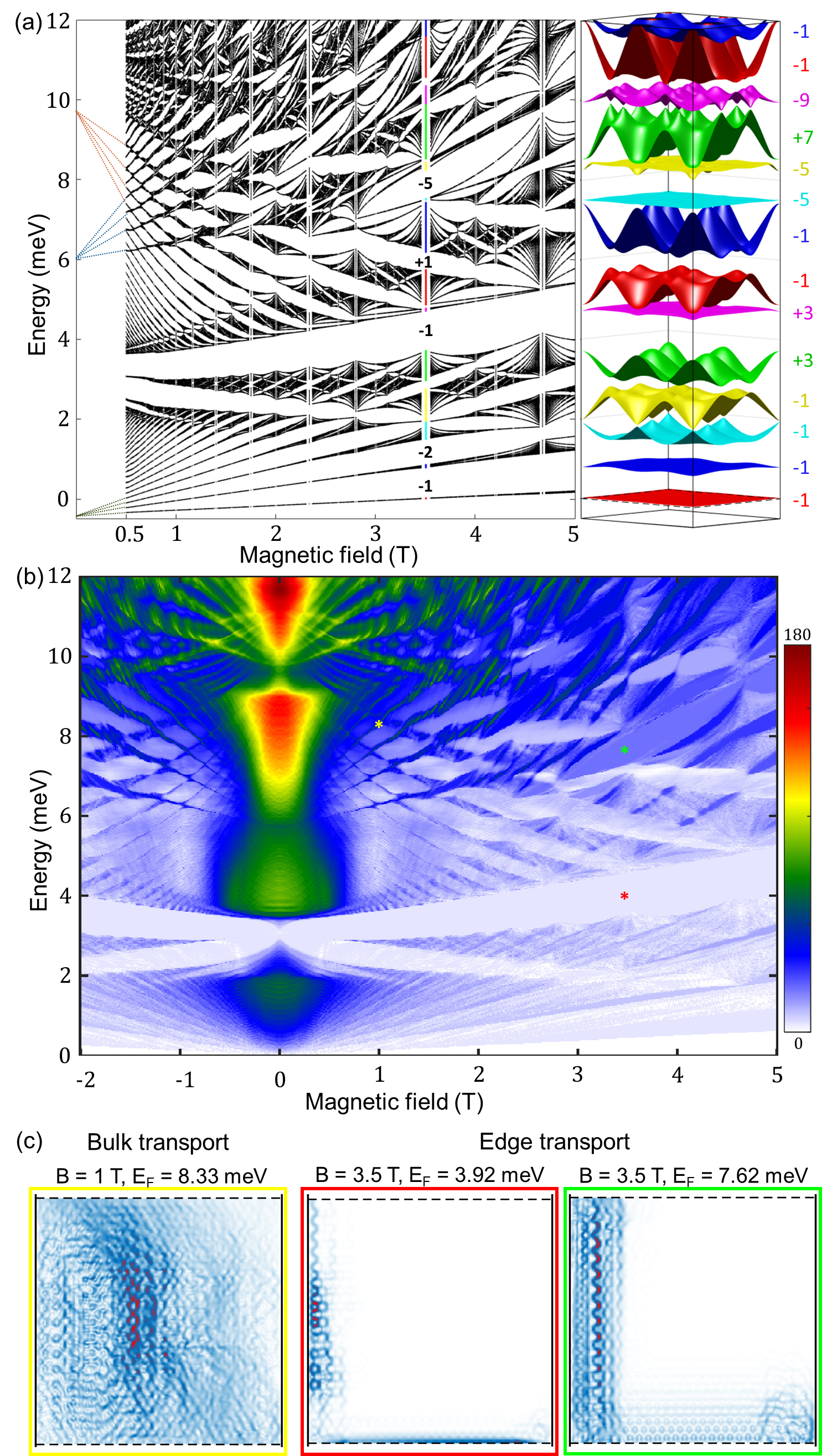
Magnetic fields induces strong reconstructions in the mini band structure described above. At very low magnetic fields, the spectrum in the conduction band turns into a series of Landau levels, linear in magnetic field, and with origins at the parabolic band edges of the non-magnetic bands, as shown in dotted lines in Fig. 2 (a). For magnetic fields T, we observe a rhomboid mesh-like structure at meV, originated from the inter-crossing of Landau levels coming from the top edge of the second and the bottom edge of the third non-magnetic mini bands. At higher magnetic fields, these rhomboid mesh develops into an intricate self-similar structure of larva-like energy windows of absence of states, which co-exists with other butterfly-like structures. We also observe two windows of empty states, separated by a fractal structure that originates from meV, which corresponds to the zeroth order Landau level of the conical dispersion in Fig. 1 (b), for very low magnetic fields.
The quantum transport simulation across a two-terminal device is shown in Fig. 2 (b). Overall, the transport map exhibits identical features to those in the Hofstadter’s butterfly computations. However, unlike in Figs. 1 (b) and (c), transport inside band gaps is not zero, but times an integer value of the fundamental conductance, . This is because gaps host topologically protected edge states, which we confirm by computing the Chern numbers associated to each magnetic mini band, for a the commensurate structure that corresponds to ( T). We checked that inside a given gap, the numerically computed value for the conductance is equal to the sum of all chern number of the bands below [shown inside the Hofstadter’s map in Fig. 2 (a)] times . Conversely, quantum transport inside the bands occurs inside the bulk. To visualise these two types of quantum transport, we present the current density amplitude plot in panel (c) of the same figure. While in bulk transport the maximum amplitude of the current density is at the centre of the sample, in edge transport, the centre of the sample features absence of states, forcing the transport to occur at the left edge of the sample.
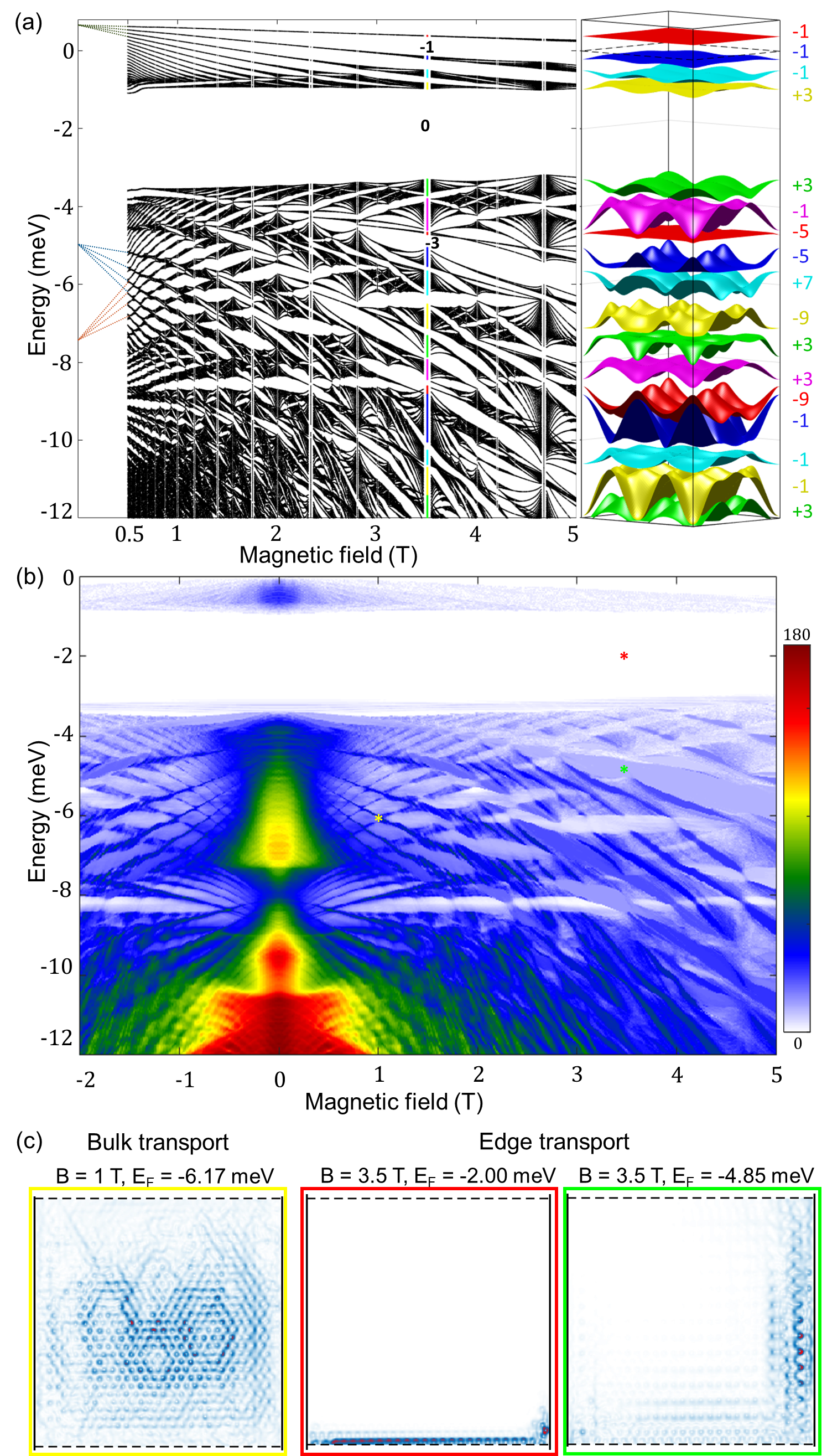
In Fig. 3 we present an analogue study for the valence band of \chMoS2. Similar features are observed in this plot: a rhomboid mesh-like structure at T produced by the inter crossing of Landau levels from different bands and the topologically protected edge states inside the gaps, inside which of the conductance is constant and equal to times the sum of the Chern number of the bands above a certain gap. Notice that, as opposed to the conduction side, the topologically trivial gap induced by the superlattice in Fig. 1 (b) is not closed by the magnetic field, and because the sum of the Chern numbers cannot change inside a given window of empty states, there is no edge states transport for , as shown in Fig 3 (c). As a consequence, the system is always a trivial insulator for a doping concentration of 4 holes per superlattice unit cell, which in our case is . This qualitative difference between the transport in n-dope and p-dope \chMoS2 is reversed for negative values of , which provides an experimental route to identify the is sign this parameter.
In conclusion, superlattice potentials induce changes on the electronic spectrum of \chMoS2 that can be traced in transport experiments, with and without magnetic fields. Our modelled superlattice potential depends only on one parameter, , the sign of which entails a qualitatively different electronic features. We have neglected the effect of spin-orbit interaction, which typically induces a band splitting. In the valence band this band splitting is of the order of meV[60], well above the range of energies considered here. Therefore, our conclusions remains unchanged for this band, with the only change in the degeneracy factor . In the conduction side, however, the band splitting is smaller. Experiments suggest it could be as low as meV [61] or as large as meV [18], and it may have a quantitative impact on our results. We leave the changes in the spectrum derived from spin-orbit coupling as the subject for future studies.
Acknowledgements.
We thank National Science and Technology Council (NSTC 112-2112-M-006-019-MY3) for financial support and National Center for High-performance Computing (NCHC) for providing computational and storage resources.
References
- Rademaker [2022] L. Rademaker, Physical Review B 105, 195428 (2022), publisher: American Physical Society, URL https://link.aps.org/doi/10.1103/PhysRevB.105.195428.
- Kogar et al. [2017] A. Kogar, M. S. Rak, S. Vig, A. A. Husain, F. Flicker, Y. I. Joe, L. Venema, G. J. MacDougall, T. C. Chiang, E. Fradkin, et al., Science 358, 1314 (2017), publisher: American Association for the Advancement of Science, URL https://www.science.org/doi/10.1126/science.aam6432.
- Gao et al. [2023] Q. Gao, Y.-h. Chan, Y. Wang, H. Zhang, P. Jinxu, S. Cui, Y. Yang, Z. Liu, D. Shen, Z. Sun, et al., Nature Communications 14, 994 (2023), ISSN 2041-1723, number: 1 Publisher: Nature Publishing Group, URL https://www.nature.com/articles/s41467-023-36667-x.
- Frindt [1972] R. F. Frindt, Physical Review Letters 28, 299 (1972), publisher: American Physical Society, URL https://link.aps.org/doi/10.1103/PhysRevLett.28.299.
- Foner and McNiff [1973] S. Foner and E. J. McNiff, Physics Letters A 45, 429 (1973), ISSN 0375-9601, URL https://www.sciencedirect.com/science/article/pii/0375960173906932.
- Khestanova et al. [2018] E. Khestanova, J. Birkbeck, M. Zhu, Y. Cao, G. L. Yu, D. Ghazaryan, J. Yin, H. Berger, L. Forro, T. Taniguchi, et al., Nano Letters 18, 2623 (2018), ISSN 1530-6984, publisher: American Chemical Society, URL https://doi.org/10.1021/acs.nanolett.8b00443.
- Rogee et al. [2022] L. Rogee, L. Wang, Y. Zhang, S. Cai, P. Wang, M. Chhowalla, W. Ji, and S. P. Lau, Science 376, 973 (2022), publisher: American Association for the Advancement of Science, URL https://www.science.org/doi/10.1126/science.abm5734.
- Weston et al. [2022] A. Weston, E. G. Castanon, V. Enaldiev, F. Ferreira, S. Bhattacharjee, S. Xu, H. Corte-Leon, Z. Wu, N. Clark, A. Summerfield, et al., Nature Nanotechnology 17, 390 (2022), ISSN 1748-3395, number: 4 Publisher: Nature Publishing Group, URL https://www.nature.com/articles/s41565-022-01072-w.
- Mak et al. [2010] K. F. Mak, C. Lee, J. Hone, J. Shan, and T. F. Heinz, Physical Review Letters 105, 136805 (2010), publisher: American Physical Society, URL https://link.aps.org/doi/10.1103/PhysRevLett.105.136805.
- Splendiani et al. [2010] A. Splendiani, L. Sun, Y. Zhang, T. Li, J. Kim, C.-Y. Chim, G. Galli, and F. Wang, Nano Letters 10, 1271 (2010), ISSN 1530-6984, publisher: American Chemical Society, URL https://doi.org/10.1021/nl903868w.
- Radisavljevic et al. [2011] B. Radisavljevic, A. Radenovic, J. Brivio, V. Giacometti, and A. Kis, Nature Nanotechnology 6, 147 (2011), ISSN 1748-3395, number: 3 Publisher: Nature Publishing Group, URL https://www.nature.com/articles/nnano.2010.279.
- Pham et al. [2019] T. Pham, G. Li, E. Bekyarova, M. E. Itkis, and A. Mulchandani, ACS Nano 13, 3196 (2019), ISSN 1936-0851, publisher: American Chemical Society, URL https://doi.org/10.1021/acsnano.8b08778.
- Kumar et al. [2020] R. Kumar, W. Zheng, X. Liu, J. Zhang, and M. Kumar, Advanced Materials Technologies 5, 1901062 (2020), ISSN 2365-709X, _eprint: https://onlinelibrary.wiley.com/doi/pdf/10.1002/admt.201901062, URL https://onlinelibrary.wiley.com/doi/abs/10.1002/admt.201901062.
- Liao et al. [2019] F. Liao, Y. Sheng, Z. Guo, H. Tang, Y. Wang, L. Zong, X. Chen, A. Riaud, J. Zhu, Y. Xie, et al., Nano Research 12, 2515 (2019), ISSN 1998-0000, URL https://doi.org/10.1007/s12274-019-2478-5.
- Taniguchi et al. [2012] K. Taniguchi, A. Matsumoto, H. Shimotani, and H. Takagi, Applied Physics Letters 101, 042603 (2012), ISSN 0003-6951, URL https://doi.org/10.1063/1.4740268.
- Hennighausen and Kar [2021] Z. Hennighausen and S. Kar, Electronic Structure 3, 014004 (2021), ISSN 2516-1075, publisher: IOP Publishing, URL https://dx.doi.org/10.1088/2516-1075/abd957.
- Goryca et al. [2019] M. Goryca, J. Li, A. V. Stier, T. Taniguchi, K. Watanabe, E. Courtade, S. Shree, C. Robert, B. Urbaszek, X. Marie, et al., Nature Communications 10, 4172 (2019), ISSN 2041-1723, number: 1 Publisher: Nature Publishing Group, URL https://www.nature.com/articles/s41467-019-12180-y.
- Pisoni et al. [2018] R. Pisoni, A. Kormanyos, M. Brooks, Z. Lei, P. Back, M. Eich, H. Overweg, Y. Lee, P. Rickhaus, K. Watanabe, et al., Physical Review Letters 121, 247701 (2018), publisher: American Physical Society, URL https://link.aps.org/doi/10.1103/PhysRevLett.121.247701.
- Cui et al. [2015] X. Cui, G.-H. Lee, Y. D. Kim, G. Arefe, P. Y. Huang, C.-H. Lee, D. A. Chenet, X. Zhang, L. Wang, F. Ye, et al., Nature Nanotechnology 10, 534 (2015), ISSN 1748-3395, number: 6 Publisher: Nature Publishing Group, URL https://www.nature.com/articles/nnano.2015.70.
- Kormanyos et al. [2015] A. Kormanyos, P. Rakyta, and G. Burkard, New Journal of Physics 17, 103006 (2015), ISSN 1367-2630, publisher: IOP Publishing, URL https://dx.doi.org/10.1088/1367-2630/17/10/103006.
- Smolenski et al. [2019] T. Smolenski, O. Cotlet, A. Popert, P. Back, Y. Shimazaki, P. Knüppel, N. Dietler, T. Taniguchi, K. Watanabe, M. Kroner, et al., Physical Review Letters 123, 097403 (2019), publisher: American Physical Society, URL https://link.aps.org/doi/10.1103/PhysRevLett.123.097403.
- Ho et al. [2015] Y.-H. Ho, W.-P. Su, and M.-F. Lin, RSC Advances 5, 20858 (2015), ISSN 2046-2069, publisher: The Royal Society of Chemistry, URL https://pubs.rsc.org/en/content/articlelanding/2015/ra/c4ra15271a.
- Hofstadter [1976] D. R. Hofstadter, Physical Review B 14, 2239 (1976), publisher: American Physical Society, URL https://link.aps.org/doi/10.1103/PhysRevB.14.2239.
- Bistritzer and MacDonald [2011a] R. Bistritzer and A. H. MacDonald, Physical Review B 84, 035440 (2011a), publisher: American Physical Society, URL https://link.aps.org/doi/10.1103/PhysRevB.84.035440.
- Hejazi et al. [2019] K. Hejazi, C. Liu, and L. Balents, Physical Review B 100, 035115 (2019), publisher: American Physical Society, URL https://link.aps.org/doi/10.1103/PhysRevB.100.035115.
- Crosse et al. [2020] J. A. Crosse, N. Nakatsuji, M. Koshino, and P. Moon, Physical Review B 102, 035421 (2020), publisher: American Physical Society, URL https://link.aps.org/doi/10.1103/PhysRevB.102.035421.
- Moon and Koshino [2012] P. Moon and M. Koshino, Physical Review B 85, 195458 (2012), publisher: American Physical Society, URL https://link.aps.org/doi/10.1103/PhysRevB.85.195458.
- Lian et al. [2021] B. Lian, F. Xie, and B. A. Bernevig, Physical Review B 103, L161405 (2021), publisher: American Physical Society, URL https://link.aps.org/doi/10.1103/PhysRevB.103.L161405.
- Fabian et al. [2022] T. Fabian, M. Kausel, L. Linhart, J. Burgdörfer, and F. Libisch, Physical Review B 106, 165412 (2022), publisher: American Physical Society, URL https://link.aps.org/doi/10.1103/PhysRevB.106.165412.
- Chen et al. [2014] X. Chen, J. R. Wallbank, A. A. Patel, M. Mucha-Kruczynski, E. McCann, and V. I. Falko, Physical Review B 89, 075401 (2014), publisher: American Physical Society, URL https://link.aps.org/doi/10.1103/PhysRevB.89.075401.
- Ponomarenko et al. [2013] L. A. Ponomarenko, R. V. Gorbachev, G. L. Yu, D. C. Elias, R. Jalil, A. A. Patel, A. Mishchenko, A. S. Mayorov, C. R. Woods, J. R. Wallbank, et al., Nature 497, 594 (2013), ISSN 1476-4687, number: 7451 Publisher: Nature Publishing Group, URL https://www.nature.com/articles/nature12187.
- Huber et al. [2020] R. Huber, M.-H. Liu, S.-C. Chen, M. Drienovsky, A. Sandner, K. Watanabe, T. Taniguchi, K. Richter, D. Weiss, and J. Eroms, Nano Letters 20, 8046 (2020), ISSN 1530-6984, publisher: American Chemical Society, URL https://doi.org/10.1021/acs.nanolett.0c03021.
- Krishna Kumar et al. [2017] R. Krishna Kumar, X. Chen, G. H. Auton, A. Mishchenko, D. A. Bandurin, S. V. Morozov, Y. Cao, E. Khestanova, M. Ben Shalom, A. V. Kretinin, et al., Science 357, 181 (2017), publisher: American Association for the Advancement of Science, URL https://www.science.org/doi/10.1126/science.aal3357.
- Krishna Kumar et al. [2018] R. Krishna Kumar, A. Mishchenko, X. Chen, S. Pezzini, G. H. Auton, L. A. Ponomarenko, U. Zeitler, L. Eaves, V. I. Fal’ko, and A. K. Geim, Proceedings of the National Academy of Sciences 115, 5135 (2018), publisher: Proceedings of the National Academy of Sciences, URL https://www.pnas.org/doi/full/10.1073/pnas.1804572115.
- Barrier et al. [2020] J. Barrier, P. Kumaravadivel, R. Krishna Kumar, L. A. Ponomarenko, N. Xin, M. Holwill, C. Mullan, M. Kim, R. V. Gorbachev, M. D. Thompson, et al., Nature Communications 11, 5756 (2020), ISSN 2041-1723, number: 1 Publisher: Nature Publishing Group, URL https://www.nature.com/articles/s41467-020-19604-0.
- Huber et al. [2022] R. Huber, M.-N. Steffen, M. Drienovsky, A. Sandner, K. Watanabe, T. Taniguchi, D. Pfannkuche, D. Weiss, and J. Eroms, Nature Communications 13, 2856 (2022), ISSN 2041-1723, number: 1 Publisher: Nature Publishing Group, URL https://www.nature.com/articles/s41467-022-30334-3.
- Yang et al. [2016] W. Yang, X. Lu, G. Chen, S. Wu, G. Xie, M. Cheng, D. Wang, R. Yang, D. Shi, K. Watanabe, et al., Nano Letters 16, 2387 (2016), ISSN 1530-6984, publisher: American Chemical Society, URL https://doi.org/10.1021/acs.nanolett.5b05161.
- Liu et al. [2013] G.-B. Liu, W.-Y. Shan, Y. Yao, W. Yao, and D. Xiao, Physical Review B 88, 085433 (2013), publisher: American Physical Society, URL https://link.aps.org/doi/10.1103/PhysRevB.88.085433.
- Fang et al. [2015] S. Fang, R. Kuate Defo, S. N. Shirodkar, S. Lieu, G. A. Tritsaris, and E. Kaxiras, Physical Review B 92, 205108 (2015), ISSN 1098-0121, 1550-235X, URL https://link.aps.org/doi/10.1103/PhysRevB.92.205108.
- Shahriari et al. [2018] M. Shahriari, A. Ghalambor Dezfuli, and M. Sabaeian, Superlattices and Microstructures 114, 169 (2018), ISSN 0749-6036, URL https://www.sciencedirect.com/science/article/pii/S0749603617329154.
- Kadantsev and Hawrylak [2012] E. S. Kadantsev and P. Hawrylak, Solid State Communications 152, 909 (2012), ISSN 0038-1098, URL https://www.sciencedirect.com/science/article/pii/S0038109812000889.
- Yankowitz et al. [2012] M. Yankowitz, J. Xue, D. Cormode, J. D. Sanchez-Yamagishi, K. Watanabe, T. Taniguchi, P. Jarillo-Herrero, P. Jacquod, and B. J. LeRoy, Nat. Phys. 8, 382 (2012), ISSN 1745-2473.
- Chen et al. [2020] S.-C. Chen, R. Kraft, R. Danneau, K. Richter, and M.-H. Liu, Commun. Phys. 3, 71 (2020).
- Kraft et al. [2020] R. Kraft, M.-H. Liu, P. B. Selvasundaram, S.-C. Chen, R. Krupke, K. Richter, and R. Danneau, Phys. Rev. Lett. 125, 217701 (2020), URL https://journals.aps.org/prl/abstract/10.1103/PhysRevLett.125.217701.
- Xian et al. [2021] L. Xian, M. Claassen, D. Kiese, M. M. Scherer, S. Trebst, D. M. Kennes, and A. Rubio, Nature Communications 12, 5644 (2021), ISSN 2041-1723, number: 1 Publisher: Nature Publishing Group, URL https://www.nature.com/articles/s41467-021-25922-8.
- Liu et al. [2014] K. Liu, L. Zhang, T. Cao, C. Jin, D. Qiu, Q. Zhou, A. Zettl, P. Yang, S. G. Louie, and F. Wang, Nature Communications 5, 4966 (2014), ISSN 2041-1723, number: 1 Publisher: Nature Publishing Group, URL https://www.nature.com/articles/ncomms5966.
- Chang et al. [2014] T.-R. Chang, H. Lin, H.-T. Jeng, and A. Bansil, Scientific Reports 4, 6270 (2014), ISSN 2045-2322, number: 1 Publisher: Nature Publishing Group, URL https://www.nature.com/articles/srep06270.
- Zhong et al. [2016] H. Zhong, R. Quhe, Y. Wang, Z. Ni, M. Ye, Z. Song, Y. Pan, J. Yang, L. Yang, M. Lei, et al., Scientific Reports 6, 21786 (2016), ISSN 2045-2322, number: 1 Publisher: Nature Publishing Group, URL https://www.nature.com/articles/srep21786.
- Liu et al. [2012] Q. Liu, L. Li, Y. Li, Z. Gao, Z. Chen, and J. Lu, The Journal of Physical Chemistry C 116, 21556 (2012), ISSN 1932-7447, publisher: American Chemical Society, URL https://doi.org/10.1021/jp307124d.
- Huang et al. [2014] S. Huang, X. Ling, L. Liang, J. Kong, H. Terrones, V. Meunier, and M. S. Dresselhaus, Nano Letters 14, 5500 (2014), ISSN 1530-6984, publisher: American Chemical Society, URL https://doi.org/10.1021/nl5014597.
- Lopes dos Santos et al. [2007] J. M. B. Lopes dos Santos, N. M. R. Peres, and A. H. Castro Neto, Physical Review Letters 99, 256802 (2007), publisher: American Physical Society, URL https://link.aps.org/doi/10.1103/PhysRevLett.99.256802.
- Bistritzer and MacDonald [2011b] R. Bistritzer and A. H. MacDonald, Proceedings of the National Academy of Sciences 108, 12233 (2011b), publisher: Proceedings of the National Academy of Sciences, URL https://www.pnas.org/doi/10.1073/pnas.1108174108.
- Koshino [2015] M. Koshino, New Journal of Physics 17, 015014 (2015), ISSN 1367-2630, publisher: IOP Publishing, URL https://dx.doi.org/10.1088/1367-2630/17/1/015014.
- Garcia-Ruiz et al. [2021] A. Garcia-Ruiz, H.-Y. Deng, V. V. Enaldiev, and V. I. Fal’ko, Physical Review B 104, 085402 (2021), publisher: American Physical Society, URL https://link.aps.org/doi/10.1103/PhysRevB.104.085402.
- Polini et al. [2013] M. Polini, F. Guinea, M. Lewenstein, H. C. Manoharan, and V. Pellegrini, Nature Nanotechnology 8, 625 (2013), ISSN 1748-3387, 1748-3395, URL https://www.nature.com/articles/nnano.2013.161.
- Krix and Sushkov [2020] Z. E. Krix and O. P. Sushkov, Physical Review B 101, 245311 (2020), ISSN 2469-9950, 2469-9969, URL https://link.aps.org/doi/10.1103/PhysRevB.101.245311.
- Chen et al. [2021] P. Chen, N. Zhang, K. Peng, L. Zhang, J. Yan, Z. Jiang, and Z. Zhong, ACS Nano 15, 13703 (2021), ISSN 1936-0851, publisher: American Chemical Society, URL https://doi.org/10.1021/acsnano.1c04995.
- Datta [1995] S. Datta, Electronic Transport in Mesoscopic Systems (Cambridge University Press, Cambridge, 1995).
- Fukui et al. [2005] T. Fukui, Y. Hatsugai, and H. Suzuki, Journal of the Physical Society of Japan 74, 1674 (2005), ISSN 0031-9015, publisher: The Physical Society of Japan, URL https://journals.jps.jp/doi/10.1143/JPSJ.74.1674.
- Zhang et al. [2015] Y. Zhang, H. Li, H. Wang, R. Liu, S.-L. Zhang, and Z.-J. Qiu, ACS Nano 9, 8514 (2015), ISSN 1936-0851, publisher: American Chemical Society, URL https://doi.org/10.1021/acsnano.5b03505.
- Marinov et al. [2017] K. Marinov, A. Avsar, K. Watanabe, T. Taniguchi, and A. Kis, Nature Communications 8, 1938 (2017), ISSN 2041-1723, number: 1 Publisher: Nature Publishing Group, URL https://www.nature.com/articles/s41467-017-02047-5.