Mass inversion at the Lifshitz transition in monolayer graphene by diffusive, high-density, on-chip, doping
Abstract
Experimental setups for charge transport measurements are typically not compatible with the ultra-high vacuum conditions for chemical doping, limiting the charge carrier density that can be investigated by transport methods. Field-effect methods, including dielectric gating and ionic liquid gating, achieve too low a carrier density to induce electronic phase transitions. To bridge this gap, we developed an integrated flip-chip method to dope graphene by alkali vapour in the diffusive regime, suitable for charge transport measurements at ultra-high charge carrier density. We introduce a cesium droplet into a sealed cavity filled with inert gas to dope a monolayer graphene sample by the process of cesium atom diffusion, adsorption and ionization at the graphene surface, with doping beyond an electron density of monitored by operando Hall measurement. The sealed assembly is stable against oxidation, enabling measurement of charge transport versus temperature and magnetic field. Cyclotron mass inversion is observed via the Hall effect, indicative of the change of Fermi surface geometry associated with the Liftshitz transition at the hyperbolic point of monolayer graphene. The transparent quartz substrate also functions as an optical window, enabling non-resonant Raman scattering. Our findings show that chemical doping, hitherto restricted to ultra-high vacuum, can be applied in a diffusive regime at ambient pressure in an inert gas environment and thus enable charge transport studies in standard cryogenic environments.
1 Introduction
The electron transport properties of nearly charge neutral graphene have been the subject of intense investigation. Much less is know about the electron transport properties of heavily electron doped graphene, where the massive, hyperbolic dispersion at the saddle points in the Brillouin zone lead to a van Hove singularity (vHS) in the density of states 1, 2, 3, 4. Angle resolved photoemission spectroscopy (ARPES) studies have mapped the Fermi surface of heavily doped monolayer graphene in the vicinity of the point 1, 5, 6, 7, 8. The role of many-body interactions in flattening and thereby extending the vHS is a matter of active debate9, 10, 11. Indeed, it can be difficult to probe many-body effects by ARPES due to the flattness of the band, further motivating investigation by complementary methods such as charge transport. The emergence of superconductivity in doped monolayer graphene prompted by strong electron-phonon coupling at the extended vHS has been the subject of theoretical inquiry 12, 13 and experimental evidence of electron-phonon coupling enhancement has been reported 14. Charge transport is one of several physical properties that are sensitive to changes in the Fermi surface geometry at a vHS 15, known as a Lifshitz transition (Fig. 1), yet no transport measurements in heavily doped graphene in the vicinity of the vHS have been reported to date.
Alkaline metal doping (Li, K, Ca, Cs) and rare earth doping (Er, Yb) of graphene in an ultra-high vacuum (UHV) environment has enabled doping in excess of for surface science studies of graphene 1, 5, 6, 7, 10, 9, 8. However, UHV environment requirements are rarely fulfilled in charge transport measurements, particularly in high magnetic field experiments. Li doping of epitaxial graphene on SiC in an integrated deposition and cryogenic charge transport measurement system was used to achieve electron densities as high as 16. Ionic liquid gating has enabled electron doping in the range of in electrically contacted graphene on Si/SiO2 substrates 17, 18, 19. Ion exchange glass has achieved doping up to with potassium20. Lithium polymer electrolytic gating has been used to achieve electron doping as high as in electrically contacted bilayer graphene 21 and can be integrated with magnetotrasport measurements. Transmission electron microscopy reveals domains with superdense Li ordering in suspended graphene bilayers corresponding to per graphene sheet 22, below the monolayer vHS threshold. There is thus a need to develop new methods that combine the advantages of chemical doping, high electron density and selection of chemical species, that can be easily integrated with existing charge transport experimental environments.
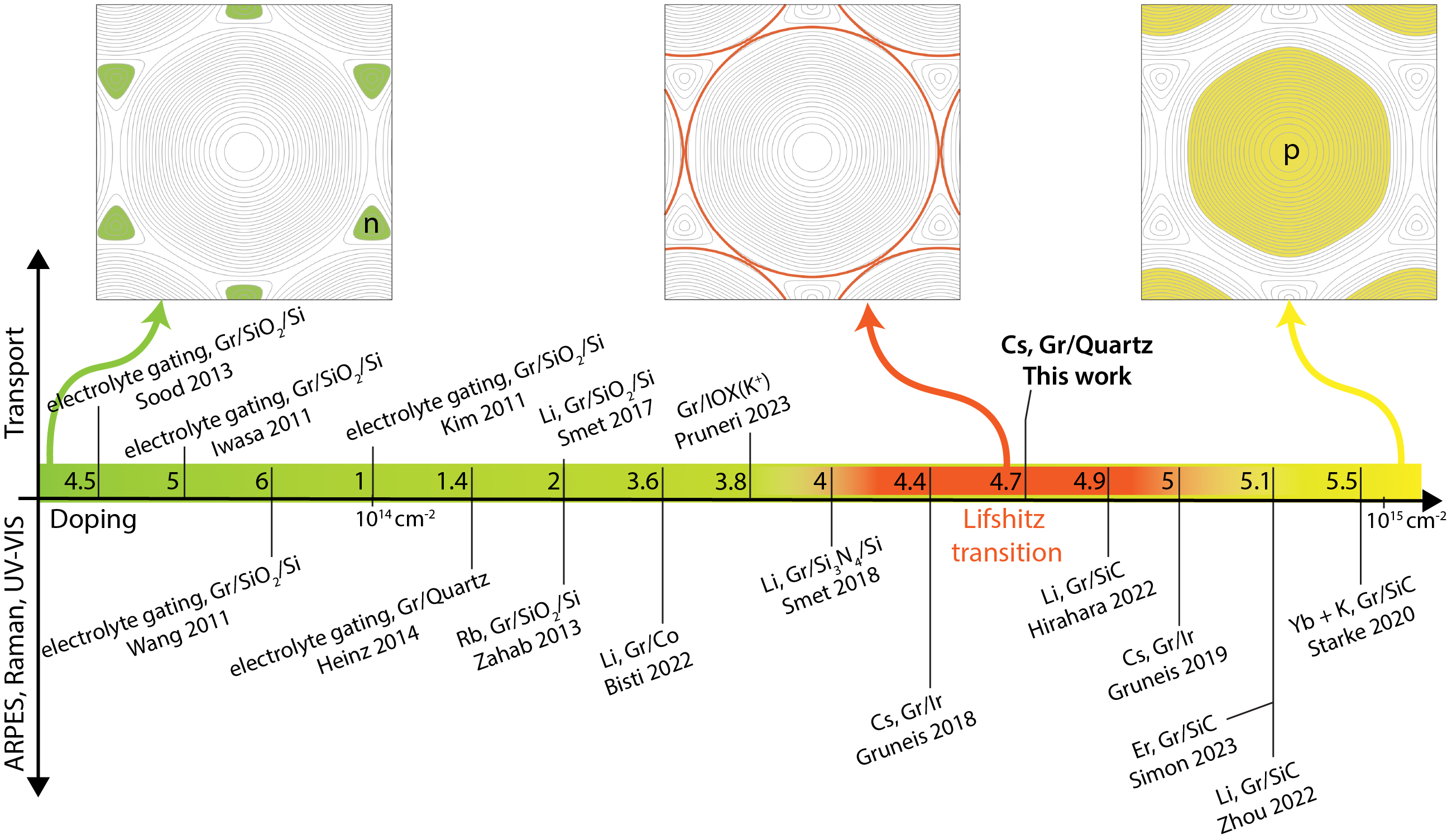
We present here an integrated flip-chip method to dope graphene by alkali vapour in the diffusive regime, suitable for charge transport measurements at ultra-high charge carrier density. The method enables operando electronic characterization and allows the hermetically sealed device to be analyzed without the requirement of UHV or inert gas environmental conditions. We demonstrate our method by doping electrically contacted large-area graphene to ultra-high charge carrier density, reaching as confirmed by the inversion of effective mass in high-field Hall measurements. This flip-chip method is versatile: it can be applied to different host material and dopant systems, and is not limited to monolayer or few-layer host materials.
The method is compatible with operando charge transport characterization during alkali doping. As shown in Fig. 2a), flip-chip encapsulation of an alkaline metal vapour source in an inert gas environment electron dopes electrically contacted graphene. The impermeability of the encapsulation to external oxidizing agents permits sample manipulation in an ambient atmospheric environment, enabling the study of heavily doped graphene by different experimental techniques. We report here operando measurements of the graphene resistivity tensor elements and in an AC magnetic field during the doping process, as well as the measurement of Hall effect, weak-localization and magnetoresistance at cryogenic temperature K at magnetic fields up to T. Cryogenic Hall measurements reveal inversion of the Hall coefficient, corresponding to the inversion of the cyclotron effective mass , where is the area subtended by the Fermi-surface 23, as expected at the Lifshitz transition at the hyperbolic point of heavily doped graphene (Fig. 1). Non-resonant Raman measurement of heavily doped graphene through the optically transparent quartz substrate reveals a peak Raman shift in agreement with previous reports of heavily doped graphene 5.
2 Experimental Methods
We used graphene grown by chemical vapour deposition (CVD) on poly-crystalline copper foil in a cold wall CVD reactor (Aixtron BM) at Graphenea, and transferred onto a 100 mm diameter quartz (001) substrate following sacrificial etch of the copper growth substrate. The graphene crystal domain size is estimated to be 1.5 m by Raman spectroscopy (see Supplementary Information). Quartz is the substrate of choice due to its chemical inertness and optical transparency. We prepare graphene Hall-bar devices using photo-lithographic methods, with Ti/Au (5 nm /80 nm) Ohmic contacts. Sonication in an acetone bath, followed by hour immersion in 1,2 dichloroethane is required to minimize organic residue contamination that may inhibit charge transfer. The six-contact Hall-bar geometry enables the simultaneous measurement of four-probe longitudinal resistance and transverse resistance .
The flip-chip method uses a ceramic chip carrier with a cavity and gold electrodes atop a recessed mesa (Fig. 2a). A drop of Cs (L in volume) is drop-cast by glass pipette into the cavity inside an inert gas glove box (H2O 0.1 ppm and O2 1 ppm). Prior to all doping experiments, we thermally annealed the Hall bar samples and chip carriers in the inert glove box environment for hours at 120∘C to remove adsorbed water. Experiments conducted in an Ar environment enabled higher doping density to be achieved than in an N2 environment. The quartz substrate with the graphene Hall bar is flipped onto the chip carrier. Pure In spheres (0.5 mm diameter) are used for reliable electrical contact between the electrodes of the chip carrier and the quartz substrate. The graphene Hall bar faces the Cs source directly and is exposed to Cs vapour within the cavity. A compact resistive heater under the chip carrier is used to increase temperature and thus Cs vapour pressure. Interestingly, these experiments are carried out in a 1 atm inert gas environment, which limits the mean free path of the Cs atoms, corresponding to a diffusive vapour transport regime as opposed to the ballistic regime of alkali doping in UHV conditions. Despite this significant difference in the vapour transport regime, we observe that similar charge carrier densities can be achieved.
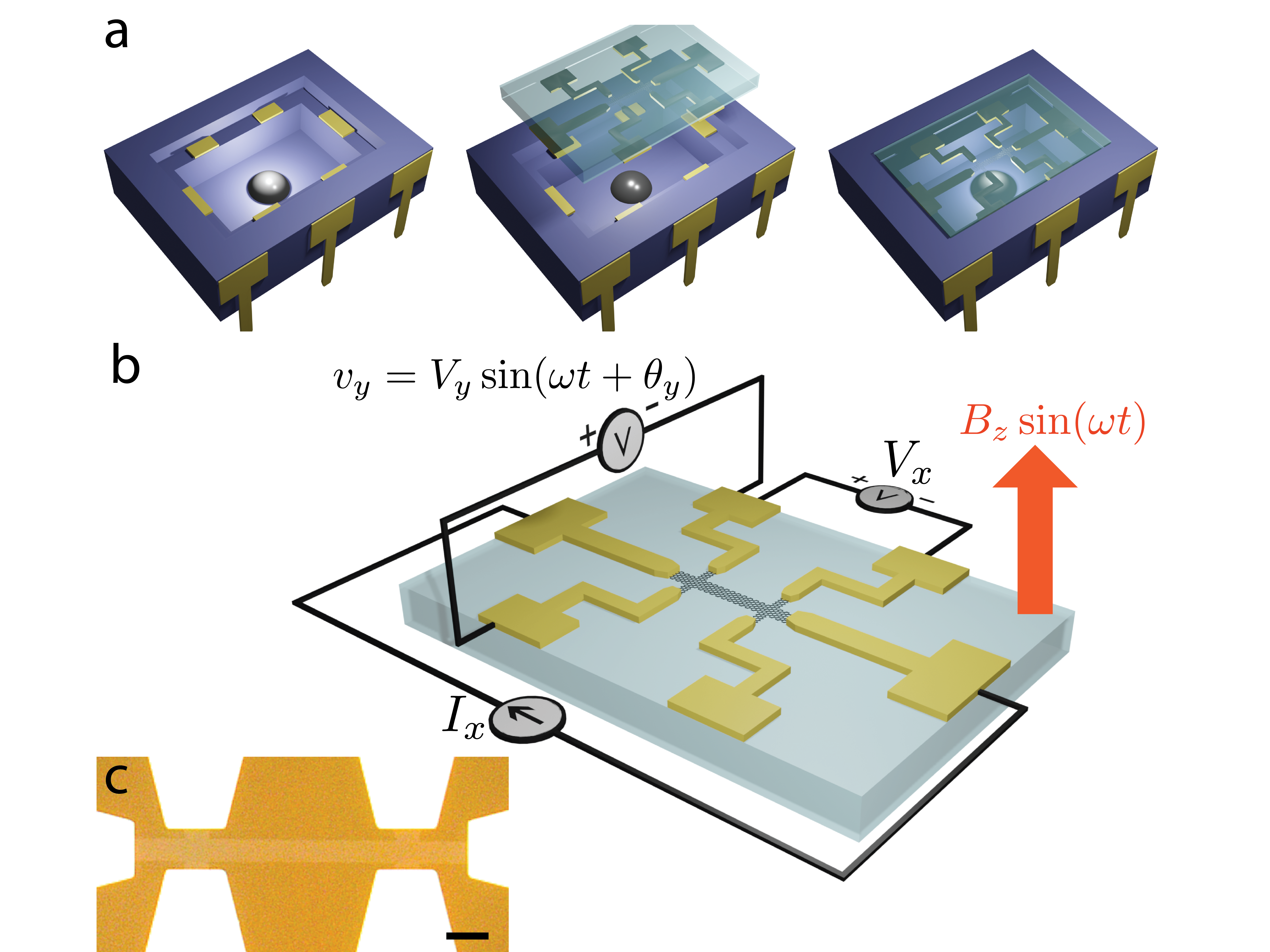
An electromagnet was used for operando Hall measurement during doping in a glove box. We used an AC-DC Hall measurement configuration (Fig. 2b) with an AC magnetic field, of amplitude = 20-25 mT and frequency Hz, and a DC sample bias current, . A similar method has been employed for Hall measurement of organic field effect transistors 24. The Hall voltage is expected to be where is 0 or according to charge carrier type. In all experiments, the direction of the bias current is selected such that Hall voltage phase () corresponds to electron (hole) doped graphene. The background inductive voltage was subtracted to obtain sample response.
Following Cs doping, we sealed the flip-chip cavity with a UV activated epoxy (Solarez) followed by potting epoxy compound (Loctite Stycast). The adhesives were degassed of oxidizing vapours in an inert gas environment prior to use. The sealed device was removed from the glove box for high magnetic field transport measurements and Raman spectroscopy. A representative optical image of a graphene Hall bar on quartz substrate is shown in Fig. 2c. High magnetic field ( = 7 T) and low-temperature ( = 1.3 K) measurement of longitudinal and transverse resistance was performed in a closed-cycle cryostat with a superconducting solenoid. Raman spectroscopy was performed with a Renishaw InVia confocal Raman microscope, 50-X magnification, nm, mW.
3 Results
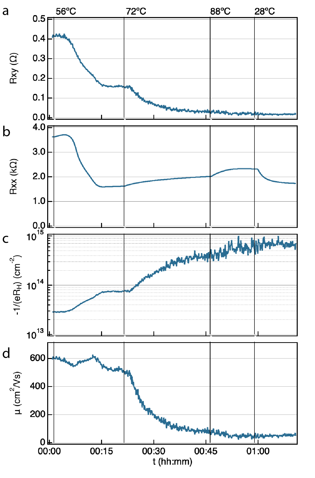
CVD grown graphene transferred onto quartz is initially p-type doped (, ), as measured by Hall effect in our samples prior to doping. During exposure to Cs vapour, ionization of adsorbed Cs atoms leads to valence electron donation to the graphene. The resistances and are shown in Fig. 3a,b during a representative Cs vapour exposure experiment. Doping is sufficiently rapid that conduction is already n-type at the beginning of the measurement. A slower doping rate in a less thoroughly cleaned graphene sample allows observation of passage through the charge neutrality point (see Supplementary Information). The Cs doping process is partially reversible, achieved by heating a doped graphene sample in Cs free chipe carrier (see Supplementary Information). The Hall coefficient can be used to directly infer charge carrier density in the case of conduction by a single charge carrier type, with for n-type graphene. The quantity and the Hall mobility , where is the graphene resistivity determined from and Hall bar geometry, versus time are shown in Fig. 3c,d. The chip carrier was heated to elevate Cs temperature, and thus Cs vapour pressure, doping rate, and doping density. Note that the Hall coefficient becomes sufficiently small upon doping that the noise limit of the operando Hall measurement is reached, and the inferred electron density exceeds the stoichiometric limit of corresponding to CsC8 observed in UHV Cs-doping experiments6. We attribute this observation to the onset of partially compensated conduction of charge carriers with positive and negative effective masses at the vHS, requiring investigation at higher magnetic field.
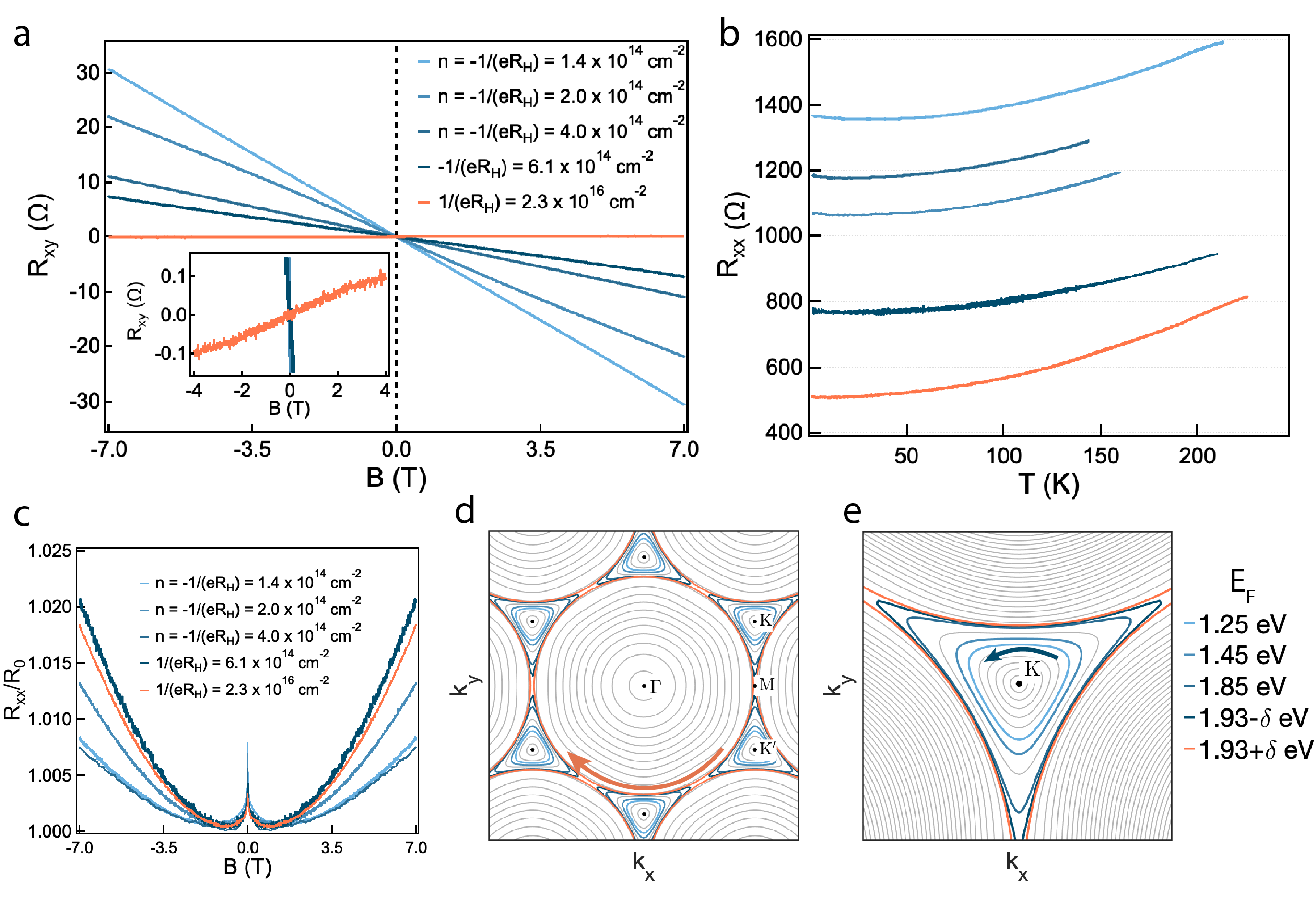
Magnetotransport experiments were conducted at high field ( T) and cryogenic temperature ( K). The Hall resistance versus is shown in Fig. 4a for five samples (identified 1-5), with an inset of the low regime. All samples show a reduction in as temperature decreases (Fig. 4b), as well as a weak localization peak and small magnetoresistance in versus (Fig. 4c). Table 1 presents a summary of the inferred charge carrier density , Hall mobility and other properties of samples 1-5. Samples 1-3 exhibit n-type behaviour with charge carrier density up to . Samples 4 and 5 exhibit a reciprocal Hall coefficient too large to be attributed to a single charge carrier type, with sample 5 exhibiting an inversion in the sign of the Hall coefficient corresponding to a change from n-type to p-type conduction.
To gain further insight into the electronic properties of these heavily doped samples, a third-nearest neighbour tight-binding (3NNTB) calculation of electronic band structure using hopping and overlap parameters determined from ARPES25 was performed. From the 3NNTB electronic structure and experimental electron density , the Fermi level was inferred, and Fermi surfaces identified in the graphene band (Fig. 4d,e). The compensated conduction of samples 4 and 5 correspond to a Fermi surface below and above, respectively, the Lifshitz transition where eV. The Hall coefficient in the vicinity of the Lifshitz transition can be understood with a simple two-band model 23 in the low-field limit,
| (1) |
where and are the Hall coefficients and conductivities of two bands. Electrons at eV for small are characterized by a Hall coefficient , where is the area around the and points enclosed by the Fermi surface in the first Brillouin zone. The factor of 2 accounts for spin degeneracy, and the numerical value of is inferred from 3NNTB calculation. Electrons at eV for small are characterized by a Hall coefficient , where is the area enclosing with opposite cyclotron motion to that of . Equivalently, the effective cyclotron mass reverses sign as crosses the vHS beyond the equi-energy contours connecting the -points, and undergoes a discontinuous change from an n-type to a p-type . With the two-band model of Eq. 1, we find that and for samples 4 and 5, respectively, corresponding to net n-type and p-type behaviour in the vicinity of the vHS. As electron doping increased, conduction in the electron pockets around and is closed and conduction in the hole pocket around is opened.
| CsCx | |||||||
|---|---|---|---|---|---|---|---|
| () | () | () | (eV) | ||||
| Sample 1 | 319 | CsC27.3 | 1.25 | 0.290 | |||
| Sample 2 | 298 | CsC19.1 | 1.45 | 0.371 | |||
| Sample 3 | 137 | CsC9.5 | 1.85 | 1.036 | |||
| Sample 4 | 38 | CsC8.1 | 1.93 - | - | |||
| Sample 5 | 59 | CsC8.1 | 1.93 + | - |
Quadratic magnetoresistance versus is observed at high field and a weak-localization peak is observed at low field. Omitting the low field regions ( T), the magnetoresistance was fit to a quadratic form . Here, is a dimensionless coefficient and is the zero-field resistance in the absence of the quantum effects, namely weak-localization. It is not possible to unambiguously identify the origin of magnetoresistance from the observation of a quadratic dependence on . The two-band conduction model 23 attributes quadratic magnetoresistance to the coexistance of a uniform distribution of two carrier types. The effective medium theory of Ping et al.26 attributes quadratic magnetoresistance to inhomogeneity in charge carrier density in graphene. If inhomogeneity in charge density leads to electron-hole puddle formation, deviation from quadratic magnetoresistance can be observed only in the limit of large magnetoresistance 27, beyond what is observable in heavily doped graphene at T.
All samples exhibited a weak localization (WL) peak in versus in the low-field regime (Fig.3c). WL occurs due to quantum coherent back-scattering of charge carriers, enhancing resistivity at T, with the effect disappearing by introduction of magnetic flux breaking the phase coherence of back-scattering events 28, 29, 30, 31, 32, 33. Weak-localization is sensitive to the contributions from multiple scattering mechanisms characterized by the following scattering lengths: phase coherence length, , intervalley scattering length, , and intravalley scattering length . The intervalley and intravalley scattering processes are illustrated schematically in Fig. 4c. The WL correction to longitudinal conductivity, , has been analytically calculated for weakly doped graphene where the Dirac cone is an accurate model for dispersion28, 29,
| (2) |
where , is the digamma function and is the flux quantum. For magnetic field T, and thus . A numerical fit of the experimental over T to Eq. 2 was used to determine the scattering lengths, with a representative example shown in Fig.5(a) for sample 5 (see Supplementary Information for other samples). The scattering lengths and versus doping density at K are shown in Fig. 5b. The magnetoresistance is less than 3% of the magnitude of the WL resistance peak for T, and error bars were determined by the fit parameter deviation that increases the sum of squares error between fit and measurement two-fold over that at optimum fit value. At K, the phase coherence lengths are in the range and the intervalley scattering lengths are in the range nm in our heavily doped graphene samples, in general agreement with previous reports of WL in graphene 30, 33, 34. The shortening of and with increasing carrier density over the range has been previously observed in monolayer graphene 34.
Being shorter than the estimated mean free path , the intravalley scattering length could not be reliably determined by fit of Eq. 2 to the experimental 32, 35. As the effective mass diverges at the Lifshitz transition, the more weakly doped samples 1-3 were used to estimate the mean free path nm, where is the Fermi velocity and the scattering time is estimated from . Nonetheless, we may observe that trigonal warping is the dominant source of intravalley scattering at densities of with an estimated scattering length 28, 34,
| (3) |
where is the graphene lattice constant and eV is the nearest-neighbour hopping energy (see Supplementary Information), corresponding to nm. This model is based on a 1NN approximation that is appropriate to weakly-doped graphene where a Dirac cone approximation to energy-momentum dispersion is accurate. A theoretical treatment of the scattering rates and lengths near the vHS of monolayer graphene has yet to be developed for doping levels close to the Lifshitz transition.
Beyond charge transport measurements, Raman spectroscopy provides an independent experimental probe of charge carrier density via the measured shift of the vibrational frequencies to the effects of lattice expansion and electron-phonon coupling. Raman Stokes spectra were measured in an series of Cs-doped graphene samples independent of those used in charge transport experiments. Fig. 6a presents the room temperature Raman spectra of several samples with different doping densities determined from AC Hall measurements. The Raman -peak position, initially at 1586 cm-1 for pristine samples with native doping, shifts up with doping and reaches a peak value of 1613 cm-1, followed by a slight downshift with further doping (Fig. 6b) in qualitative agreement with previous experimental observations of ionic liquid gated graphene36, 37, 38, Rb-doped graphene on SiO2 39, and Cs-doped graphene on Ir 5, and first-principles calculations of the phonon hardening / softening 40. Further insight can be obtained by comparison of the observed -peak shift, , relative to pristine samples with the model of Hell et al.5,
| (4) |
where the static contribution, , is associated with lattice expansion and adiabatic electron-phonon coupling, is the ratio of static -peak shift of graphene in the presence of graphene-substrate interactions to that of an ideally decoupled graphene, and the dynamic contribution, , is associated with non-adiabatic electron-phonon coupling effects. The static contribution is estimated with an analytic approximation to numerical calculation 40. The dynamic contribution is determined by numerical calculation of the electron-phonon coupling 40, using 3NNTB electronic structure 25 and the deformation potential, derived from ARPES analysis of Cs doped graphene 5 (see Supplementary Information). A fit of the experimentally observed to the model of Eq. 4, shown in Fig. 6b gives agreement with . In comparison with Cs doped graphene on Ir (111), where was found 5, the interaction of graphene transferred to quartz suppresses lattice expansion to a lesser degree than epitaxial graphene on Ir (111).
Increased Cs-doping also suppresses the () peak intensity relative to the peak intensity (Fig. 4a), in agreement with experiments with ionic liquid gated doped graphene 37, 19 and Rb-doped graphene 39. We used pump excitation at nm ( eV) to minimize fluorescence. At this excitation energy, as illustrated in Fig. 4c, and Raman scattering is strongly detuned from resonance. Under the highly detuned conditions of our experiments, the () peak intensity is expected to be diminished to a greater extent than the peak intensity as detuning increases with doping, since the () and processes are 2nd order and 1st order, respectively. In summary, Raman spectroscopy provides an independent confirmation of the high doping achieved in Cs doped graphene produced in this study.
4 Conclusion
We have demonstrated a comparatively facile method utilizing an inert glove box environment for doping graphene to a high charge carrier density, up to , approaching the stoichiometric limit CsC8, and sufficient to observe effective mass inversion at the Lifshitz transition of monolayer graphene. The method permits operando charge transport characterization during alkali doping, and enables further experimental characterization by methods such as magnetotransport and Raman spectroscopy. Surprisingly, this method shows that the charge densities that can be achieved by alkali doping in a diffusive vapour transport regime are similar to those achieved in UHV conditions. The charge carrier density reached by this method exceeds previous reports, and is thus anticipated to enable studies of highly doped few-layer materials, complementing ARPES studies of highly doped systems on metallic substrates. The extension of the doping method presented here to other alkali dopants and target materials and devices may provide a new means of exploring the physics of highly doped low-dimensional systems such as heavily doped black phosphorus which have been shown to exhibit bandgap modulation, closure, and inversion owing to an unusually strong Stark effect 41, 42, or alkali doped C60 to synthesize high critical temperature superconductors 43. In terms of commercial applications, the flip-chip method can be implemented to dope microfabricated ion traps designed for quantum computing 44.
5 Acknowledgements
A.M.A., O.D., S.N.R.B. and T.S. acknowledge financial support from the Natural Sciences and Engineering Research Council of Canada (RGPIN-2018-04851,ALLRP-571923-22), Fonds de recherche du Québec – Nature et technologies (299633), and technical assistance from the Laboratoire de Microfabrication, École Polytechnique, Montréal. A.G. acknowledges Deutsche Forschungsgemeinschaft projects SE2575/4 and GR3708/4-1.
References
- McChesney et al. 2010 McChesney, J. L.; Bostwick, A.; Ohta, T.; Seyller, T.; Horn, K.; González, J.; Rotenberg, E. Extended van Hove singularity and superconducting instability in doped graphene. Physical Review Letters 2010, 104, 136803
- Kravets et al. 2010 Kravets, V.; Grigorenko, A.; Nair, R.; Blake, P.; Anissimova, S.; Novoselov, K.; Geim, A. Spectroscopic ellipsometry of graphene and an exciton-shifted van Hove peak in absorption. Physical Review B 2010, 81, 155413
- Mak et al. 2011 Mak, K. F.; Shan, J.; Heinz, T. F. Seeing many-body effects in single-and few-layer graphene: observation of two-dimensional saddle-point excitons. Physical Review Letters 2011, 106, 046401
- Mak et al. 2014 Mak, K. F.; Da Jornada, F. H.; He, K.; Deslippe, J.; Petrone, N.; Hone, J.; Shan, J.; Louie, S. G.; Heinz, T. F. Tuning many-body interactions in graphene: The effects of doping on excitons and carrier lifetimes. Physical Review Letters 2014, 112, 207401
- Hell et al. 2018 Hell, M. G.; Ehlen, N.; Senkovskiy, B. V.; Hasdeo, E. H.; Fedorov, A.; Dombrowski, D.; Busse, C.; Michely, T.; Di Santo, G.; Petaccia, L.; others Resonance Raman spectrum of doped epitaxial graphene at the Lifshitz transition. Nano Letters 2018, 18, 6045–6056
- Ehlen et al. 2020 Ehlen, N.; Hell, M.; Marini, G.; Hasdeo, E. H.; Saito, R.; Falke, Y.; Goerbig, M. O.; Di Santo, G.; Petaccia, L.; Profeta, G.; Gruneis, A. Origin of the Flat Band in Heavily Cs-Doped Graphene. ACS Nano 2020, 14, 1055–1069
- Rosenzweig et al. 2020 Rosenzweig, P.; Karakachian, H.; Marchenko, D.; Küster, K.; Starke, U. Overdoping graphene beyond the van Hove singularity. Physical Review Letters 2020, 125, 176403
- Zaarour et al. 2023 Zaarour, A.; Malesys, V.; Teyssandier, J.; Cranney, M.; Denys, E.; Bubendorff, J.; Florentin, A.; Josien, L.; Vonau, F.; Aubel, D.; others Flat band and Lifshitz transition in long-range-ordered supergraphene obtained by Erbium intercalation. Physical Review Research 2023, 5, 013099
- Bao et al. 2022 Bao, C.; Zhang, H.; Wu, X.; Zhou, S.; Li, Q.; Yu, P.; Li, J.; Duan, W.; Zhou, S. Coexistence of extended flat band and Kekulé order in Li-intercalated graphene. Physical Review B 2022, 105, L161106
- Ichinokura et al. 2022 Ichinokura, S.; Toyoda, M.; Hashizume, M.; Horii, K.; Kusaka, S.; Ideta, S.; Tanaka, K.; Shimizu, R.; Hitosugi, T.; Saito, S.; others Van Hove singularity and Lifshitz transition in thickness-controlled Li-intercalated graphene. Physical Review B 2022, 105, 235307
- Jugovac et al. 2022 Jugovac, M.; Tresca, C.; Cojocariu, I.; Di Santo, G.; Zhao, W.; Petaccia, L.; Moras, P.; Profeta, G.; Bisti, F. Clarifying the apparent flattening of the graphene band near the van Hove singularity. Physical Review B 2022, 105, L241107
- Profeta et al. 2012 Profeta, G.; Calandra, M.; Mauri, F. Phonon-mediated superconductivity in graphene by lithium deposition. Nature Physics 2012, 8, 131–134
- Nandkishore et al. 2012 Nandkishore, R.; Levitov, L. S.; Chubukov, A. V. Chiral superconductivity from repulsive interactions in doped graphene. Nature Physics 2012, 8, 158–163
- Ludbrook et al. 2015 Ludbrook, B.; Levy, G.; Nigge, P.; Zonno, M.; Schneider, M.; Dvorak, D.; Veenstra, C.; Zhdanovich, S.; Wong, D.; Dosanjh, P.; others Evidence for superconductivity in Li-decorated monolayer graphene. Proceedings of the National Academy of Sciences 2015, 112, 11795–11799
- Kaganov and Lifshits 1979 Kaganov, M. I.; Lifshits, I. M. Electron theory of metals and geometry. Soviet Physics Uspekhi 1979, 22, 904
- Khademi et al. 2019 Khademi, A.; Kaasbjerg, K.; Dosanjh, P.; Stöhr, A.; Forti, S.; Starke, U.; Folk, J. A. Weak localization measurements of electronic scattering rates in Li-doped epitaxial graphene. Physical Review B 2019, 100, 161405
- Efetov and Kim 2010 Efetov, D. K.; Kim, P. Controlling electron-phonon interactions in graphene at ultrahigh carrier densities. Physical Review Letters 2010, 105, 256805
- Ye et al. 2011 Ye, J.; Craciun, M. F.; Koshino, M.; Russo, S.; Inoue, S.; Yuan, H.; Shimotani, H.; Morpurgo, A. F.; Iwasa, Y. Accessing the transport properties of graphene and its multilayers at high carrier density. Proceedings of the National Academy of Sciences 2011, 108, 13002–13006
- Chen et al. 2011 Chen, C. F.; Park, C. H.; Boudouris, B. W.; Horng, J.; Geng, B.; Girit, C.; Zettl, A.; Crommie, M. F.; Segalman, R. A.; Louie, S. G.; Wang, F. Controlling inelastic light scattering quantum pathways in graphene. Nature 2011, 471, 617–20
- Graham et al. 2023 Graham, C.; Marchena, M.; Paulillo, B.; Bhattacharyya, I.; Mazumder, P.; Pruneri, V. Highly doped graphene on ion-exchanged glass. 2D Materials 2023, 10, 035037
- Kühne et al. 2017 Kühne, M.; Paolucci, F.; Popovic, J.; Ostrovsky, P. M.; Maier, J.; Smet, J. H. Ultrafast lithium diffusion in bilayer graphene. Nature Nanotechnology 2017, 12, 895
- Kühne et al. 2018 Kühne, M.; Börrnert, F.; Fecher, S.; Ghorbani-Asl, M.; Biskupek, J.; Samuelis, D.; Krasheninnikov, A. V.; Kaiser, U.; Smet, J. H. Reversible superdense ordering of lithium between two graphene sheets. Nature 2018, 564, 234–239
- Ashcroft and Mermin 1976 Ashcroft, N. W.; Mermin, N. D. Solid State Physics,; Holt Saunders International, 1976
- Chen et al. 2016 Chen, Y.; Yi, H. T.; Podzorov, V. High-Resolution AC Measurements of the Hall Effect in Organic Field-Effect Transistors. Physical Review Applied 2016, 5, 034008
- Grüneis et al. 2008 Grüneis, A.; Attaccalite, C.; Wirtz, L.; Shiozawa, H.; Saito, R.; Pichler, T.; Rubio, A. Tight-binding description of the quasiparticle dispersion of graphite and few-layer graphene. Physical Review B 2008, 78, 205425
- Ping et al. 2014 Ping, J.; Yudhistira, I.; Ramakrishnan, N.; Cho, S.; Adam, S.; Fuhrer, M. S. Disorder-induced magnetoresistance in a two-dimensional electron system. Phys Rev Lett 2014, 113, 047206
- Cho and Fuhrer 2008 Cho, S.; Fuhrer, M. S. Charge transport and inhomogeneity near the minimum conductivity point in graphene. Physical Review B 2008, 77, 081402
- McCann et al. 2006 McCann, E.; Kechedzhi, K.; Fal’ko, V. I.; Suzuura, H.; Ando, T.; Altshuler, B. L. Weak-localization magnetoresistance and valley symmetry in graphene. Phys Rev Lett 2006, 97, 146805
- Fal’ko et al. 2007 Fal’ko, V. I.; Kechedzhi, K.; McCann, E.; Altshuler, B.; Suzuura, H.; Ando, T. Weak localization in graphene. Solid State Communications 2007, 143, 33–38
- Morozov et al. 2006 Morozov, S. V.; Novoselov, K. S.; Katsnelson, M.; Schedin, F.; Ponomarenko, L.; Jiang, D.; Geim, A. K. Strong suppression of weak localization in graphene. Physical Review Letters 2006, 97, 016801
- Tikhonenko et al. 2008 Tikhonenko, F.; Horsell, D.; Gorbachev, R.; Savchenko, A. Weak localization in graphene flakes. Physical Review Letters 2008, 100, 056802
- Tikhonenko et al. 2008 Tikhonenko, F.; Horsell, D.; Wilkinson, B.; Gorbachev, R.; Savchenko, A. The effect of inter-valley scattering on weak localisation in graphene. Physica E: Low-dimensional Systems and Nanostructures 2008, 40, 1364–1366
- Ki et al. 2008 Ki, D.-K.; Jeong, D.; Choi, J.-H.; Lee, H.-J.; Park, K.-S. Inelastic scattering in a monolayer graphene sheet: A weak-localization study. Physical Review B 2008, 78, 125409
- Baker et al. 2012 Baker, A. M. R.; Alexander-Webber, J. A.; Altebaeumer, T.; Janssen, T. J. B. M.; Tzalenchuk, A.; Lara-Avila, S.; Kubatkin, S.; Yakimova, R.; Lin, C. T.; Li, L. J.; Nicholas, R. J. Weak localization scattering lengths in epitaxial, and CVD graphene. Physical Review B 2012, 86, 235441
- Lara-Avila et al. 2011 Lara-Avila, S.; Tzalenchuk, A.; Kubatkin, S.; Yakimova, R.; Janssen, T.; Cedergren, K.; Bergsten, T.; Fal’ko, V. Disordered Fermi liquid in epitaxial graphene from quantum transport measurements. Physical review letters 2011, 107, 166602
- Pisana et al. 2007 Pisana, S.; Lazzeri, M.; Casiraghi, C.; Novoselov, K. S.; Geim, A. K.; Ferrari, A. C.; Mauri, F. Breakdown of the adiabatic Born-Oppenheimer approximation in graphene. Nat Mater 2007, 6, 198–201
- Das et al. 2008 Das, A.; Pisana, S.; Chakraborty, B.; Piscanec, S.; Saha, S. K.; Waghmare, U. V.; Novoselov, K. S.; Krishnamurthy, H. R.; Geim, A. K.; Ferrari, A. C.; Sood, A. K. Monitoring dopants by Raman scattering in an electrochemically top-gated graphene transistor. Nat Nanotechnol 2008, 3, 210–5
- Froehlicher and Berciaud 2015 Froehlicher, G.; Berciaud, S. Raman spectroscopy of electrochemically gated graphene transistors: Geometrical capacitance, electron-phonon, electron-electron, and electron-defect scattering. Physical Review B 2015, 91, 205413
- Parret et al. 2013 Parret, R.; Paillet, M.; Huntzinger, J.-R.; Nakabayashi, D.; Michel, T.; Tiberj, A.; Sauvajol, J.-L.; Zahab, A. A. In situ Raman probing of graphene over a broad doping range upon rubidium vapor exposure. ACS nano 2013, 7, 165–173
- Lazzeri and Mauri 2006 Lazzeri, M.; Mauri, F. Nonadiabatic Kohn anomaly in a doped graphene monolayer. Phys Rev Lett 2006, 97, 266407
- Kim et al. 2015 Kim, J.; Baik, S. S.; Ryu, S. H.; Sohn, Y.; Park, S.; Park, B.-G.; Denlinger, J.; Yi, Y.; Choi, H. J.; Kim, K. S. Observation of tunable band gap and anisotropic Dirac semimetal state in black phosphorus. Science 2015, 349, 723–726
- Ehlen et al. 2018 Ehlen, N.; Sanna, A.; Senkovskiy, B.; Petaccia, L.; Fedorov, A.; Profeta, G.; Grüneis, A. Direct observation of a surface resonance state and surface band inversion control in black phosphorus. Physical Review B 2018, 97, 045143
- Zong et al. 2022 Zong, L.-N.; Wang, R.-S.; Peng, D.; Chen, X.-J. Superconductivity in Nonstoichiometric Rubidium-Doped C60. The Journal of Physical Chemistry C 2022, 126, 2912–2919
- Auchter et al. 2022 Auchter, S.; Axline, C.; Decaroli, C.; Valentini, M.; Purwin, L.; Oswald, R.; Matt, R.; Aschauer, E.; Colombe, Y.; Holz, P.; Monz, T.; Blatt, R.; Schindler, P.; Rössler, C.; Home, J. Industrially microfabricated ion trap with 1 eV trap depth. Quantum Science and Technology 2022, 7, 035015