A parametrically programmable delay line for microwave photons
Abstract
Delay lines capable of storing quantum information are crucial for advancing quantum repeaters and hardware efficient quantum computers. Traditionally, they are physically realized as extended systems that support wave propagation, such as waveguides. But such delay lines typically provide limited control over the propagating fields. Here, we introduce a parametrically addressed delay line (PADL) for microwave photons that provides a high level of control over the dynamics of stored pulses, enabling us to arbitrarily delay or even swap pulses. By parametrically driving a three-waving mixing superconducting circuit element that is weakly hybridized with an ensemble of resonators, we engineer a spectral response that simulates that of a physical delay line, while providing fast control over the delay line’s properties and granting access to its internal modes. We illustrate the main features of the PADL, operating on pulses with energies on the order of a single photon, through a series of experiments, which include choosing which photon echo to emit, translating pulses in time, and swapping two pulses. We also measure the noise added to the delay line from our parametric interactions and find that the added noise is much less than one photon.
Delay lines that preserve quantum information have been proposed as a resource for universal, fault-tolerant, hardware-efficient quantum computing [1, 2]. Although microwave superconducting circuits are a leading platform for building a quantum computer, implementing a delay line in these systems is challenging. For example, a superconducting coplanar waveguide (CPW) on silicon would need to be meters in length to provide a s delay.
Several innovative approaches have been developed to circumvent traditional delay lines’ substantial physical length requirements. The first of these employs slow-wave or slow-light structures, which effectively reduce the speed of electromagnetic wave propagation by using metamaterials [3] or resonator arrays [4, 5]. This technique allows for a significant decrease in the physical size of the delay line while maintaining its function. The second approach involves using waves that are not electromagnetic. A classic example is acoustic waves, such as those used by early mercury delay lines [6], and more recent Surface Acoustic Wave (SAW) technologies [7] which have been applied for delaying quantum information [8]. These methods use waves with inherently slower propagation speeds, in this case acoustic, to achieve the desired delay in a reasonable amount of space. Lastly, approaches that use atoms or emitters based on Electromagnetically Induced Transparency (EIT) [9], or those using atomic frequency combs (AFCs) [10, 11] have been developed in the last decades with a view towards quantum information. The latter AFC schemes are noteworthy as they emulate the response of a traditional delay line through light-matter interactions facilitated by pump fields. They realize what is in effect a virtual delay line – even if the system behaves as if a localized pulse is propagating down a waveguide, in reality the excitation is in the coherences of a large number of atoms and may be distributed in space and frequency in a manner that does not resemble a localized propagating pulse. The unique advantage here lies in the ability to alter the characteristics of the delay line simply by modifying the pump fields, offering a dynamic solution for implementing a more robust and versatile delay line.
In this study, we introduce a Parametrically Addressed Delay Line (PADL) as a versatile virtual delay line for microwave photons, leveraging pump fields that drive parametric processes to dynamically control the speed, direction, coupling strength, and connection points of the signal within the line. We implement the delay line by realizing an ensemble of resonators that are parametrically coupled to a lumped element readout mode. Controlling all of the delay line’s properties translates to controlling the parametric drive frequencies, amplitudes, and phases. We show how a parametric delay line gives us more control than a physical waveguide by: (1) controlling the drive amplitudes to selectively choose the number of round trips that a wavepacket makes inside the delay line, (2) controlling the drive phases to translate the pulse in time, and (3) controlling the drive detunings to swap two wavepackets in time. A key question is how the delay line will perform for quantum pulses, and whether the PADL’s parametric nature leads to excess noise, such as through parasitic processes, to degrade performance. For this, we measure the added noise from the parametric drives by calibrating the gain of our measurement apparatus using our resonators as quantum microwave parametric oscillators (MPOs) [12] that operate as quantum-calibrated sources of microwave radiation. Specifically, we use the number of photons in our quantum MPO near threshold as an in-situ noise power calibration device [13], and find that the added noise is much less than one photon per mode.
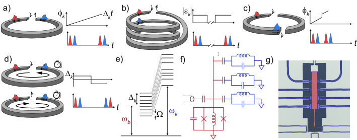
Fig. 1 illustrates the operational principle of the PADL and its analogy to a physical waveguide delay line. A reflectively terminated waveguide probed at one end appears as a collection of harmonically placed modes with detunings where and where is the free spectral range (FSR). These modes evolve by accruing a phase and rephase after a round-trip time , as shown in Fig. 1a. The PADL emulates this phase response by using a number of parametric drives. In Fig. 1b, we illustrate how we can effectively disconnect the waveguide from the input/output by shutting off the parametric drives, i.e., setting their amplitudes . This prevents the rephased signal from being emitted into the environment and causes it to propagate around the waveguide for longer. Turning the drives back on reconnects the waveguide to the environment and causes the pulse to be re-emitted at the next round-trip time for some positive integer . This mode of operation is analogous to fiber loop buffers which have been recently considered for storing quantum information [14]. Full control over the phases of the drives allows us arbitrary access to information stored in the delay line. In Fig. 1c, we illustrate how we continuously translate the pulse forwards or backwards in time by an amount (modulo ) by translating each phase by . This is analogous to accessing the pulse at positions other than the open port in a physical waveguide. In Fig. 1d, we illustrate how controlling the parametric drive detunings allows us to swap two pulses in time. Specifically, changing is equivalent to taking in terms of the phase that the delay line modes accrue. This is analogous to switching the pulse propagation direction. While we focus on these four experiments, one can engineer more complicated pulse dynamics with the novel degree of control provided by a parametric delay line.
We implement the PADL by coupling an ensemble of resonators (with arbitrarily distributed frequencies ) to a lumped element readout mode (with frequency , which we refer to as the buffer mode) via parametric drives as shown in Fig. 1e. By controlling the parametric drives, we engineer the buffer mode’s spectrum to emulate the characteristics of a reflective delay line. We achieve this by parametrically placing the modes at evenly spaced detunings and tuning the drive amplitudes to realize the desired loading. We implement the physical circuit on-chip by fabricating eight quarter-wavelength CPW resonators that are weakly capacitively coupled with a nonlinear resonant circuit known as an Asymmetrically Threaded SQUID (ATS) [15]. Crucially, the CPW frequencies do not need to be precisely placed or tuned – we use the parametric drive frequencies to compensate for any disorder to realize the mode spacing [16]. The circuit diagram is illustrated in Fig. 1f, where we illustrate the CPW resonators by their equivalent lumped element LC models. A false-color optical micrograph of the PADL device is shown in Fig. 1g, where the ATS is highlighted in red and the CPW resonators are highlighted in blue (see Appendix A for details on fabricating this device).
The ATS provides the lumped element buffer mode that we use to readout our pulses, as well as the necessary nonlinearity to parametrically couple the different modes of our circuit. We choose to use an ATS for three reasons. Firstly, the ATS provides three-wave mixing as opposed to four-wave mixing – the native nonlinearity of Josephson junctions. Three-wave mixing allows us to parametrically swap between the ATS lumped element mode and the CPW modes while minimizing the adverse effects from four-wave-mixing interactions that are characteristic of a multimode systems connected to junctions. Secondly, the ATS has an inductor, and therefore its lumped element mode can be strongly driven before it becomes nonlinear. Finally, we can use the three-wave mixing nonlinearity to implement a quantum MPO in the CPWs, which we can use for noise power calibration.
When the ATS is precisely biased at its “saddle-point,” the energy associated with the phase drop across the junctions changes from the usual to . This crucial modification shifts the dominant nonlinear term from to . As elaborated in Appendix B, we use this altered nonlinearity to enable the three-wave mixing processes essential for the operations conducted here. The Hamiltonian at the saddle-point is
| (1) |
where is the node flux zero-point fluctuation (ZPF) of the buffer mode across the ATS Josephson junctions with annihilation operator and frequency . Similarly is the ZPF of the CPW resonator fundamental mode at the same circuit node with annihilation operator and frequency . is the individual junction energy in the SQUID, and is a time-dependent parametric flux pump threading the SQUID. Note that we have assumed .
We resonantly select specific interactions by driving the buffer mode while simultaneously flux pumping the SQUID. We focus here on a beamsplitter interaction between the buffer mode and the CPW’s fundamental mode. We flux pump the SQUID at a single frequency and drive the buffer mode with multiple drives tones, as captured by the following driving Hamiltonian:
| (2) |
Here, is the frequency of a detuned drive on the buffer with field amplitude . We choose the drive frequencies to satisfy
| (3) |
In the frame where both the CPW mode and the buffer are rotated out, our total Hamiltonian approximately becomes [17]:
| (4) |
where is the parametric coupling strength between the buffer and the CPW’s fundamental mode, and is the small displacement on generated by the drive. By operating the buffer in the fast-cavity regime, i.e., , we can adiabatically eliminate it. We tune the drive amplitudes and frequencies so that the and harmonically placed in the resulting effective Hamiltonian closely resemble that of a delay line. Importantly, by controlling the parametric drives’ frequency, amplitude, and phase, we control the corresponding delay line mode’s detuning, coupling, and phase.
The ATS parameters are chosen such that GHz and GHz (see Appendix C for more details). The buffer is capacitively coupled to the environment at a rate MHz. We estimate from finite element electromagnetic simulations (see Appendix C for more details) that the buffer impedance and hybridization strengths with the CPWs leads to flux ZPF across the junction for each mode of roughly and .
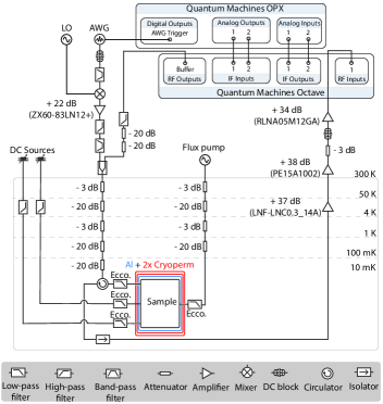
We first start with the simplest PADL experiment – implementing a response that mimics that of a reflectively terminated transmission line probed at the other end. For this, we tune and fix the parametric drives’ amplitudes, phases, and detunings (as illustrated in Fig. 1a) for seven of the CPWs 111For all the experiments in this work, we only parametrically couple seven of the eight CPW resonators to the buffer as we observed one of the CPW modes to have larger frequency fluctuations, which we attribute to a nearby two-level system (TLS) defect.. We set the FSR to be so the delay line bandwidth closely matches the buffer mode’s extrinsic coupling rate. The continuous wave (CW) pump tone is provided by a signal generator (Keysight E8257D PSG). The parametric drive intermediate frequency (IF) tones are all generated on a single arbitrary waveform generator (AWG) channel (Tektronix 5200) before being up-converted to drive the buffer mode. Before being up-converted, the AWG output is amplified by a room-temperature low-noise amplifier (see Appendix D for more details). All pulses sent into the delay line are played, demodulated, and digitized using an Operator-X (OPX) from Quantum Machines Inc. (QM), and similarly the pulses are up-converted and down-converted using an Octave from QM (see Appendix D for more details).
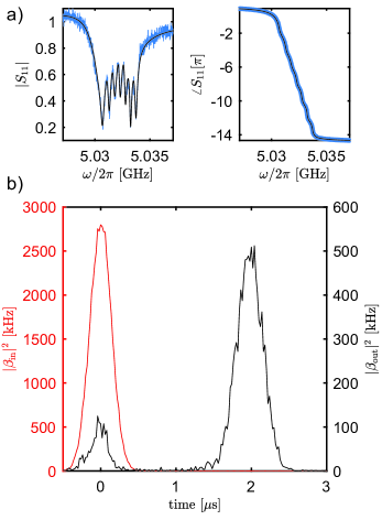
We probe the PADL on reflection near the buffer mode frequency and clearly observe the parametrically coupled modes in the normalized reflection coefficient (Fig. 2a). We tune the parameters to obtain an approximately linear phase response centered at GHz to emulate the phase response of a physical delay line. We measure the time-domain response by sending pulses at the PADL. Fig. 2b shows the results of reflecting an attenuated Gaussian pulse (, with a temporal FWHM of 471 ns; see Appendix H for more details on the calibration of the attenuation). The red pulse centered at results from reflecting a pulse off of the device in the absence of pump and drives and with the buffer mode far-detuned, so that the device acts as a mirror. The black pulse results from reflecting a pulse off the buffer mode while the device is emulating a delay line. We observe that the pulse is approximately delayed by . The small reflected pulse at in the black trace is due to mismatched impedance between the environment and the parametric delay line, including any inevitable mismatches from device packaging (see Appendix G for more details). The time-domain traces are reported in units of photon flux.
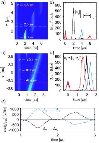
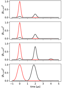
By turning the parametric drive amplitudes off, we prevent a stored wavepacket from being emitted, causing the pulse to undertake another round trip in the delay line. Turning the amplitudes back on allows the next photon echo to be emitted. In Fig. 3a, we sweep the duration over which we turn off the parametric drive amplitude. Delay corresponds to the drives being on continuously. We see that as exceeds , the first echo disappears and the second echo at becomes more prominent. Similarly, as exceeds , the second photon echo disappears and the third photon echo at becomes more prominent. In Fig. 3b, we show the ADC data of traces taken with = s (black), s (blue), and s (red).
We fine-tune the photon emission time by modifying the parametric drive phases . By changing these phases we continuously translate the pulse in time, as illustrated in Fig. 1c. Specifically, by translating , we can translate our pulse by a time modulo . In Fig. 3c, we sweep the duration by which we translate our pulse, where corresponds continuous parametric driving without phase modification. We see that as we sweep , the time at which at the pulse re-emits translates linearly. In Fig. 3d, we show the ADC data of traces taken with = s (black), s (red), and s (blue).
Finally, we show how controlling the parametric drive detunings allows us to swap two pulses in time, as illustrated in Fig. 1d. Swapping the detunings , is analogous to performing time reversal in the phase accrued by the delay line modes, causing the first stored pulse to be emitted after the second pulse. In Fig. 3e, we show two complex ADC traces: one where the detunings are swapped (blue) and one where they are not (black). In this experiment, we send two pulses with FWHM = ns and separation of ns. We make the first pulse have a phase shift relative to the second pulse and plot one quadrature of the measured ADC data to clearly show that the two pulses are swapped in order when the detunings are swapped. The black trace in Fig. 3e plots the case where the detunings are not swapped, corresponding to the case of continuous drives. The blue trace in Fig. 3e plots the case where the detunings are swapped, corresponding to the case where we take . We clearly see that relative to the black trace, the pulses have been swapped.
An important figure of merit in quantum memories is the fidelity of the state being read out compared to that which was stored. Ideally, the output pulse should be identical in amplitude and phase to the input pulse. In reality, distortions and loss induced by storage in the PADL and thermal noise reduce the fidelity. We will show that the latter is negligible in our system, and first focus on distortion and loss. Given two pulses that are characterized by temporal mode operators and , we define the fidelity as . Here, is the temporal mode profile for the input pulse, while is the temporal mode profile for the delayed pulse. We calculate these mode profiles by normalizing the detected field measured on the ADC. The input mode is always normalized such that corresponding to unit detection probability. To isolate the impact of distortions on the pulse while it is stored in the PADL, we first normalize the delayed pulse such that . We also exclusively focus on the pulse centered at and neglect contributions from the small reflected pulse at , which can be caused by impedance mismatches in the device packaging. Ignoring losses, we measure . Time-domain simulations of the semi-classical equations of motion for and derived from Eq. 4 show that fidelity can be further improved by optimizing the parametric delay line parameters and input pulse bandwidth (see Appendix G for more details). To include the effect of losses, we normalize by the same factor that we normalize resulting in . In this case, we find a that includes both loss and distortion, showing that the infidelity is primarily due to losses in the storage resonators.
In addition to loss and distortion, an important concern is whether the parametric driving of the PADL leads to excess noise being added to the microwave field. We estimate the added noise by measuring the power spectral density of the field emitted at the CPW mode frequencies when the drives are on. The key challenge is to calibrate the gain and loss in the readout signal path with sufficient precision to be able to infer the microwave fluctuations at the device from the field detected outside the fridge. Previously, this has been accomplished by using in-situ calibrated sources, such as shot noise tunnel junctions [19] or qubits [20]. In both these cases, the physics of the source is sufficiently well-understood to provide a signal with a well-defined photon flux or noise power without requiring a component-by-component accounting of gain and loss. Here we use the device itself, operated as a parametric oscillator, as such a quantum calibrated source. In a classical model of a parametric oscillator there is a discontinuity at the oscillation threshold. This discontinuity is smoothed away by the fluctuations of the electromagnetic field in a more accurate quantum model of a parametric oscillator. The dependence of number of intracavity photons vs. drive power obtains a characteristic shape [21, 13] which we use to infer the number of photons and calibrate the gain of our amplification chain (see Appendix H for more details).
We implement the MPO on the same device by pumping the ATS at to resonantly select a 2-photon swapping term given by . After adiabatically eliminating the fast-decaying buffer mode and applying a resonant drive, the effective dynamics of the CPW mode are governed by a Lindblad master equation , with the Hamiltonian and loss operators given by
| (5) |
In these equations, is the two-photon drive strength, is the two-photon loss rate, and is the single-photon loss rate.
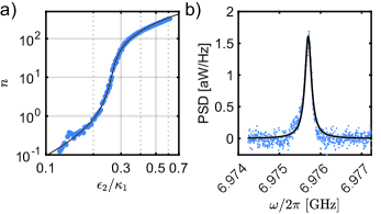
In Fig. 4a, we show how the steady-state CPW intracavity photon number changes with the amplitude of the normalized two-photon drive when we operate one of the CPWs (the resonator at 6.975562 GHz) as a quantum MPO. We measure the integrated power spectral density (PSD), which is proportional to , on an RF spectrum analyzer and plot the result versus the amplitude of the driving field sent to the buffer mode. A smooth transition is clearly visible and the data agrees closely with the quantum model of the MPO (eqn. 5) with three fitting parameters: (1) the proportionality constant between and the driving field at the instrument, (2) the proportionality constant between and the integrated PSD at the instrument, which is related to the gain, and (3) .
With the gain calibrated, we can determine the number of added noise photons. In Fig. 4b, we show the spectrum of the same CPW resonator as in Fig. 4a but now with the parametric drives and pump for the delay line experiments turned on. By fitting this spectrum to a Lorentzian to extract the spectral area and by using our calibrated gain, we conclude that 0.11 noise photons are added to this mode when it is operated as the PADL. We find that the added noise in all modes is always less than 0.15 photons for the reported drive intensities. The added noise is probably due to our strong parametric flux pump. This pump power is comparable to previous quantum-limited parametric amplifiers [22, 23] and is likely comparable to previous ATS-based devices with higher quality-factor resonators demonstrating cat states [15, 24]. Therefore, we do not believe this small added noise will hinder future quantum applications for the PADL.
Unlike a waveguide delay line, the PADL gives us complete control over the detunings, phases, and coupling rates of the delay line modes. Furthermore, delays that are comparable to a several kilometer long waveguide can be achieved for microwave photons in a small footprint. Unlike catch-and-release methods that require a single resonant mode and precise mode matching via dynamic and precisely timed control of cavity parameters, PADL offers far greater flexibility. By using a three-wave mixing circuit element we sidestep issues due to parasitic processes that arise more frequently in four-wave mixing schemes. In lieu of performing process tomography on encoded qubits, we characterize the bosonic channel by measuring the number of photons of noise that are added into our delay line as well as the overlap between the input and output wavepackets. We demonstrate dynamic programmability by selecting emission of later photon echos, translating pulses continuously in time, and swapping two pulses stored in the emulated delay line. Finally we stress that more intricate control can be engineered, given that the PADL is fully programmable, and that integration with qubits is a possibility. In future work, integration with recently developed ultra-high-Q microwave cavities [25, 26] coupled to ATSs [15, 13, 24] may open the route to long programmable delays in quantum processors with much higher fidelity than demonstrated here. In addition to memories being essential for emerging quantum network applications, such devices may enable more hardware efficient approaches to quantum information processing [1, 2].
Acknowledgements
The authors thank O. Hitchcock, R. Gruenke, M. Maksymowych, T. Rajabzadeh, Z. Wang, W. Jiang, F. Mayor, S. Malik, S. Gyger, and E. A. Wollack for useful discussions and assistance with fabrication. The authors thank K. Villegas and T. Gish from QM for their assistance with the Octave and OPX. Device fabrication was performed at the Stanford Nano Shared Facilities (SNSF) and the Stanford Nanofabrication Facility (SNF), supported by the NSF award ECCS-2026822. TM acknowledges support from the National Science Foundation Graduate Research Fellowship Program (grant no. DGE-1656518).
Appendix A: Device Fabrication
Our device is patterned in aluminum on m thick high-resistivity silicon ( 10 kcm). The sample is first solvent cleaned in acetone and isopropyl alcohol, followed by the following four-mask process:
-
1.
Etched alignment marks: Alignment marks are patterned with photolithography (Heidelberg MLA150 direct-writer) and etched into the sample using XeF2. The sample is then cleaned in baths of piranha (3:1 H2SO4:H2O2) and buffered oxide etchant.
-
2.
Circuit patterning: Ground planes, CPWs, flux lines, and the ATS island are patterned with photolithography, followed by a gentle oxygen plasma. Aluminum is deposited in an electron beam evaporator (Plassys) and lifted off in N-Methyl-2-pyrrolidone (NMP).
-
3.
Junction patterning: The ATS itself (including the SQUID loop and the superinductor) are patterned by electron beam lithography (Raith Voyager), followed by a gentle oxygen plasma. Aluminum is deposited at an angle of 62∘, followed by oxidation at 50 Torr for 10 minutes, followed by aluminum deposition at an angle of 0∘. Liftoff is performed in NMP.
-
4.
Bandaging: We use a bandage mask to ensure a superconducting connection between the previous two masks. The bandages are patterned with electron beam lithography and overlap both masks. Prior to aluminum deposition (at 0∘), we ion-mill in-situ to clear away any oxide, thus ensuring a superconducting connection. Liftoff is performed in NMP.
Appendix B: Circuit Analysis
The ATS consists of a SQUID (with individual junction energies ) that is threaded by an inductor (with energy ). In terms of the node flux operator of the ATS node, the potential from the inductor and SQUID can be written as:
| (6) |
where:
| (7) |
| (8) |
and where and are the external magnetic fluxes threading the left and right loops formed by the inductor and a Josephson junction [15, 13, 24].
When the device is flux-biased to and a small RF modulation is applied to , the potential (to first order in ) becomes:
| (9) |
Since the ATS is capacitively coupled to other modes, the node flux operator representing the flux across the junction can be written in terms of the normal modes of the linear circuit as:
| (10) |
where is the node flux ZPF of the “buffer-like” normal mode, and is the node flux ZPF of the “CPW-like” normal mode of the CPW mode [27]. The full Hamiltonian is then:
| (11) |
as dicussed in the main text.
Microwave Parametric Amplification: When is pumped at a frequency , we need to look for terms in the Hamiltonian that can resonate with this frequency. They are of the form [17]:
These terms represent processes where two photons from the CPW mode are either absorbed or emitted in combination with the emission or absorption of a photon from the buffer-like mode.
Beamsplitter operation: Alternatively, when is pumped at a frequency , and a second drive at frequency is applied to the buffer, we will implement a beam splitter interaction between the buffer-like mode and the CPW mode. In this setup, the interaction Hamiltonian can be simplified to terms that resonate with the combined effect of both drives. The resonant terms in this case are [17]:
Appendix C: Device Parameters
Our device parameters are summarized in Table 1. To determine for the CPW resonators and for the buffer mode, we simulate the capacitive coupling between the CPWs and the buffer and fit the inductance of the ATS junction array that reproduces the measured buffer mode frequency. We leave the ATS junction array and SQUID junctions open in our capacitance simulation. We find the ATS junction array inductance to be = 7.50 nH. This values agrees within 8% of values computed from room-temperature resistance measurements (using the Ambegaokar-Baratoff formula) of nominally identical junctions that are fabricated near the device. The SQUID junction energy is also inferred from room-temperature measurements.
Given the capacitance matrix, the ATS inductance, and by treating the quarter-wavelength CPW resonators as effective lumped element LC resonators (based on their designed characteristic impedances and lengths), we can diagonalize the circuit to find the eigenfrequencies and ZPFs at the ATS node. We find that our calculated eigenfrequencies agree well with our measured frequencies (within 1%). The resulting eigenvectors are used to compute and .
The buffer mode and the CPW modes are characterized using spectroscopy with a vector network analyzer when the buffer is flux biased at the saddle point. The measured values are reported in Table 1. The buffer frequency, extrinsic loss, and intrinsic loss are respectively labeled by , , . The CPW frequencies, extrinsic losses, and intrinsic losses are respectively labeled by , , .
| 5.0073 GHz | |
|---|---|
| 7.50 nH | |
| 0.336 | |
| 3.9527 MHz | |
| 128.23 kHz | |
| 5.28 GHz |
| [GHz] | [kHz] | [kHz] | |
|---|---|---|---|
| 6.904939 | 0.0186 | 36.9077 | 31.9779 |
| 6.975562 | 0.0228 | 39.8118 | 29.0615 |
| 7.156324 | 0.0210 | 69.7096 | 41.0523 |
| 7.247145 | 0.0175 | 56.6518 | 34.0546 |
| 7.318975 | 0.0179 | 74.4013 | 39.3084 |
| 7.389379 | 0.0186 | 101.8696 | 25.0361 |
| 7.460333 | 0.0211 | 131.4977 | 67.0512 |
Appendix D: Experimental details and setup
The experimental setup is shown in Fig. 5. Here, we describe the main components of our experiment: (1) parametric driving of the buffer mode, (2) playing and digitizing pulses, (3) DC flux biasing, and (4) flux pumping.
Parametric driving of the buffer mode: We use a 5 GS/s AWG to simultaneously play the seven drive tones that parametrically couple the CPW resonators to the buffer mode. Each individual drive tone had a ranging from 3.3 mV to 27 mV depending on the detuning. These tones are amplified after up-conversion to provide strong enough driving on the buffer mode. The output is combined with the output of the QM OPX and Octave.
Playing and digitizing pulses: We use a QM OPX and Octave to generate Gaussian pulses that we store in the PADL. The pulses are synthesized and played from the Analog Outputs on the OPX, which are then up-converted using mixers and local oscillators (LOs) in the Octave. The Octave conveniently calibrates its internal mixers to remove spurious tones from the LO. The up-converted pulse is played from the RF Outputs on the Octave. Similarly, the Octave down-converts pulses after they interact with our device. Specifically, pulses incident on the RF Inputs are down-converted and played from the IF Outputs, which are then sent to the Analog Inputs on the OPX.
DC flux biasing: As shown in Fig. 1g, we have two flux lines that are symmetrically placed on either side of the ATS. We use two voltage sources (SRS SIM928) to bias these two flux lines. The flux lines are low-pass filtered at the 4 K stage of our dilution refrigerator (Aivon Therma-24G).
Flux pumping: As shown in Fig. 1g, we have one additional flux line that is placed directly underneath the ATS (where the ATS is grounded). This flux line provides a magnetic flux that symmetrically threads both ATS loops, thereby providing the parametric flux pump . This flux pump is sourced from a power signal generator (Keysight E8257D PSG).
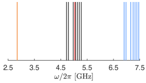
In Fig 6 we illustrate all the relevant frequencies for our experiment. We show the CPW frequencies in blue (from Table 1) and the buffer frequency in red (from Table 2). We also show the parametric drive frequencies in black, which are (in GHz): 4.719403, 4.789553, 4.971818, 5.062160, 5.132469, 5.202372, 5.276428. Finally, we show the pump frequency in orange, which is 2.84654 GHz.
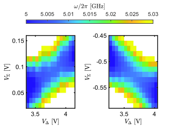
Appendix E: DC Flux Biasing
We use the two DC flux lines to find the so-called saddle point where . In Fig. 7, we show the frequency of the buffer mode in the vicinity of the saddle point as we sweep our two voltage supplies. We work in the basis of and , where and are the voltages of the individual voltage supplies.
In reality, slight junction asymmetry between the two SQUID junctions can lead to slight differences in the buffer frequency at different saddle points given by . In Fig. 7a and 7b, we show two different saddle points taken at two different values of . Fortunately, we find these two saddle point frequencies agree within a linewidth of the buffer mode. We also confirmed this at saddle points taken at two different values of . Therefore, we neglect contributions from junction asymmetry in this work.
Appendix F: Parametric Delay Line Parameters
The scattering parameters in Fig. 2a are fit to the following model model:
| (12) |
where is the buffer frequency, is the buffer extrinsic loss rate, is the buffer total loss rate, is the parametric coupling between the buffer and the CPW, is the frequency of the photons from the CPW that are being parametrically coupled to the buffer, and is the total loss rate of the CPW.
The fit parameters are listed in Table 2. In the first column, we list the CPW frequencies from Table 1 to index each row. The reported uncertainties are standard deviations from repeatedly measuring 500 times overnight and fitting the parameters.
| [GHz kHz] | 5.031227 70 |
|---|---|
| [MHz kHz] | 3.374 70 |
| [kHz kHz] | 443 60 |
| [GHz] | [GHz kHz] | [kHz kHz] | [kHz kHz] |
|---|---|---|---|
| 6.904939 | 5.032140 1 | 67 6 | 525 20 |
| 6.975562 | 5.032625 4 | 78 8 | 526 20 |
| 7.156324 | 5.031112 9 | 109 7 | 542 10 |
| 7.247145 | 5.031607 4 | 90 8 | 557 10 |
| 7.318975 | 5.033132 5 | 125 10 | 518 20 |
| 7.389379 | 5.033617 4 | 135 20 | 521 10 |
| 7.460333 | 5.030584 10 | 212 30 | 522 20 |
Appendix G: Dominant sources of infidelity
Given two temporal modes that are defined by annihilation operators and , we define the fidelity as [28]. This is the fidelity associated with two single-photon wavepackets and . Even though we are not encoding quantum information in single-photon wavepackets, we can still estimate this fidelity from the detected field, i.e., the complex digitized data collected by the ADC. We first turn off the pumps and tune the buffer mode off resonance. The device acts as a mirror which reflects the input pulse. Our ADC records the reflected signal and averages the measured field to find , corresponding to the mean field in the reflected pulse. We then operate the PADL in the delay line mode, and record , corresponding to the mean field of delayed pulse. We normalize both of these averaged traces by the same constant such that . Fidelity for a given delay is then calculated by . We find that fidelity is maximized for , so that which is very nearly . Note that in the above formulation, since we are using the same normalization constant for both the input and output fields, the fidelity captures the effects of both loss and distortion.
We can simulate this whole process by numerically integrating the equations of motion for and derived from the Hamiltonian in Eq. 4. This allows us to estimate the dominant sources of fidelity loss in our delay line. The equations of motion are given by:
| (13) |
Since these differential equations are linear, we can take the expected values of the fields, and obtain exact mean field equation for and . The input and output photon fluxes incident on the buffer mode can be obtained from the input-output boundary condition .
In Fig. 8a, we plot the input photon flux in red and output photon flux in black for different parametric delay line parameters. In the top figure, we simulate the Hamiltonian parameters from our experiment, which are reported in Table 2. We choose to be a Gaussian pulse with temporal FWHM of ns to match the experiment. The black trace agrees well with the results measured by our ADC in Fig. 2, and we calculate a state fidelity of . For our fidelity calculation, we normalize the input mode profile () such that , and we normalize the delayed mode profile () by the same factor. In Fig. 8b, we set and find that the fidelity improves to . In Fig. 8c, we set all intrinsic loss channels to zero i.e. and find that the fidelity improves to . Finally, In Fig. 8d, we consider a lossless delay line where the Hamiltonian parameters are chosen such that is evenly spaced from to over 7 modes and fix 562.4 kHz (roughly corresponding to a frequency comb with finesse = 1.5). We also increase the pulse temporal FWHM to 942 ns, which improves the fidelity to .
In Fig. 8a, we also observe a small reflected pulse at in the parametrically delayed (black) trace. This small reflected pulse was present throughout our experiments. This is due to the slight impedance mismatch that arises from our non-ideal phase response. We observe significant reduction in this reflected pulse when we optimize our Hamiltonian parameters and increase our pulse bandwidth, as can be seen in Fig. 8d. One challenge we faced in preparing a perfect parametric delay line (i.e. a perfectly linear phase response) is the challenge of rapidly and reliably fitting while tuning the parametric drive amplitudes and detunings, especially given the large number of parameters to fit. Another source of reflections at could be inevitable impedance mismatches in our device packaging, most notably from the wirebond connecting our readout line to the PCB.
Appendix H: Gain, Attenuation, and Added noise calibration
To bound the number of added noise photons caused by strongly driving our device, we first need to carefully calibrate the gain of our measurement apparatus. To do this, we need an in-situ noise source, i.e. some way to relate the number of on-chip quanta to a measurable value at room-temperature.
In our system, we leverage the three-wave mixing interaction of the ATS to operate our CPW resonators as MPOs. We use the number of resonator photons near threshold as our in-situ noise source. The smooth increase in vs. driving field observed in our quantum MPO is similar to the behaviour of a laser near threshold [29, 30, 31].
To operate the CPW as an MPO, we pump our device at a frequency and drive our buffer at a frequency . To find where the pump and drive frequencies precisely satisfy these energy conservation relations, we sweep them and measure the spectrum of the CPW resonator. Far below threshold, is only nonzero if the pump and drive frequencies are resonant [13].
Once we have determined our resonant pump and drive frequencies, we measure the spectrum of the CPW resonator at different drive strengths. We fit the integrated PSD vs. the drive strength to a master equation model with Hamiltonian and jump operators and given by
| (14) |
where is the two-photon drive strength, is the two-photon loss rate, and is the single-photon loss rate. An example for the mode at 6.9756 GHz is shown in Fig. 4a.
| [GHz] | Gain [dB] | ||
|---|---|---|---|
| 6.904939 | 95.70 | 8.406e-4 | 0.143 |
| 6.975562 | 96.53 | 22.09e-4 | 0.092 |
| 7.156324 | 94.72 | 6.323e-4 | 0.109 |
| 7.247145 | 94.59 | 5.523e-4 | 0.143 |
| 7.318975 | 96.07 | 7.165e-4 | 0.083 |
| 7.389379 | 96.78 | 12.73e-4 | 0.065 |
| 7.460333 | 99.11 | 70.65e-4 | 0.021 |
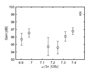
Our only fit parameters are: (1) the proportionality constant between and the driving field, (2) the proportionality constant between and the integrated PSD, which is related to the gain, and (3) . By normalizing everything with respect to , our fits are robust to pump-induced effects that may worsen . In Fig. 9, we plot our measured gain (in dB) at the different CPW frequencies (error bars are the standard deviation from repeated measurements and fits). The gain is the proportionality constant between the integrated PSD at room temperature and the power leaking out of the MPO (). We also report our fitted gains and in Table 3.
With the gain calibrated near the CPW frequencies, we can bound the noise added from strongly driving our device. Specifically, we turn on the parametric pump and drives that we use for our delay line experiments while measuring the CPW spectra. An example of such a spectrum is shown in Fig. 4b. In Table 3 we report the added noise in each CPW mode and observe it to be much less than 1 photon per mode. In the first column, we list the CPW frequencies from Table 1 to index each row.
References
- Pichler et al. [2017] H. Pichler, S. Choi, P. Zoller, and M. D. Lukin, Universal photonic quantum computation via time-delayed feedback, Proceedings of the National Academy of Sciences 114, 11362 (2017).
- Wan et al. [2021] K. Wan, S. Choi, I. H. Kim, N. Shutty, and P. Hayden, Fault-tolerant qubit from a constant number of components, PRX Quantum 2, 040345 (2021).
- Ferreira et al. [2021] V. S. Ferreira, J. Banker, A. Sipahigil, M. H. Matheny, A. J. Keller, E. Kim, M. Mirhosseini, and O. Painter, Collapse and revival of an artificial atom coupled to a structured photonic reservoir, Physical Review X 11, 041043 (2021).
- Bao et al. [2021] Z. Bao, Z. Wang, Y. Wu, Y. Li, C. Ma, Y. Song, H. Zhang, and L. Duan, On-demand storage and retrieval of microwave photons using a superconducting multiresonator quantum memory, Physical Review Letters 127, 010503 (2021).
- Yariv et al. [1999] A. Yariv, Y. Xu, R. K. Lee, and A. Scherer, Coupled-resonator optical waveguide:? a proposal and analysis, Optics letters 24, 711 (1999).
- Auerbach et al. [1949] I. L. Auerbach, J. P. Eckert, R. F. Shaw, and C. B. Sheppard, Mercury delay line memory using a pulse rate of several megacycles, Proceedings of the IRE 37, 855 (1949).
- Maines and Paige [1976] J. Maines and E. G. Paige, Surface-acoustic-wave devices for signal processing applications, in IEEE Proceedings, Vol. 64 (1976) pp. 639–652.
- Bienfait et al. [2019] A. Bienfait, K. J. Satzinger, Y. Zhong, H.-S. Chang, M.-H. Chou, C. R. Conner, É. Dumur, J. Grebel, G. A. Peairs, R. G. Povey, et al., Phonon-mediated quantum state transfer and remote qubit entanglement, Science 364, 368 (2019).
- Eisaman et al. [2005] M. D. Eisaman, A. André, F. Massou, M. Fleischhauer, A. S. Zibrov, and M. D. Lukin, Electromagnetically induced transparency with tunable single-photon pulses, Nature 438, 837 (2005).
- Afzelius et al. [2009] M. Afzelius, C. Simon, H. De Riedmatten, and N. Gisin, Multimode quantum memory based on atomic frequency combs, Physical Review A 79, 052329 (2009).
- Afzelius et al. [2010] M. Afzelius, I. Usmani, A. Amari, B. Lauritzen, A. Walther, C. Simon, N. Sangouard, J. Minář, H. De Riedmatten, N. Gisin, et al., Demonstration of atomic frequency comb memory for light with spin-wave storage, Physical review letters 104, 040503 (2010).
- Wang et al. [2019] Z. Wang, M. Pechal, E. A. Wollack, P. Arrangoiz-Arriola, M. Gao, N. R. Lee, and A. H. Safavi-Naeini, Quantum dynamics of a few-photon parametric oscillator, Physical Review X 9, 021049 (2019).
- Berdou et al. [2023] C. Berdou, A. Murani, U. Reglade, W. C. Smith, M. Villiers, J. Palomo, M. Rosticher, A. Denis, P. Morfin, M. Delbecq, et al., One hundred second bit-flip time in a two-photon dissipative oscillator, PRX Quantum 4, 020350 (2023).
- Lee et al. [2023] K. F. Lee, G. Gul, Z. Jim, and P. Kumar, Fiber loop quantum buffer for photonic qubits, arXiv preprint arXiv:2309.07987 (2023).
- Lescanne et al. [2020] R. Lescanne, M. Villiers, T. Peronnin, A. Sarlette, M. Delbecq, B. Huard, T. Kontos, M. Mirrahimi, and Z. Leghtas, Exponential suppression of bit-flips in a qubit encoded in an oscillator, Nature Physics 16, 509 (2020).
- Lee et al. [2020] N. R. Lee, M. Pechal, E. A. Wollack, P. Arrangoiz-Arriola, Z. Wang, and A. H. Safavi-Naeni, Propagation of microwave photons along a synthetic dimension, Physical Review A 101, 053807 (2020).
- Chamberland et al. [2022] C. Chamberland, K. Noh, P. Arrangoiz-Arriola, E. T. Campbell, C. T. Hann, J. Iverson, H. Putterman, T. C. Bohdanowicz, S. T. Flammia, A. Keller, et al., Building a fault-tolerant quantum computer using concatenated cat codes, PRX Quantum 3, 010329 (2022).
- Note [1] For all the experiments in this work, we only parametrically couple seven of the eight CPW resonators to the buffer as we observed one of the CPW modes to have larger frequency fluctuations, which we attribute to a nearby two-level system (TLS) defect.
- Spietz et al. [2003] L. Spietz, K. Lehnert, I. Siddiqi, and R. Schoelkopf, Primary electronic thermometry using the shot noise of a tunnel junction, Science 300, 1929 (2003).
- Macklin et al. [2015] C. Macklin, K. O’brien, D. Hover, M. Schwartz, V. Bolkhovsky, X. Zhang, W. Oliver, and I. Siddiqi, A near–quantum-limited josephson traveling-wave parametric amplifier, Science 350, 307 (2015).
- Wang [2015] Z. Wang, Coherent Computation in Degenerate Optical Parametric Oscillators (Stanford University, 2015).
- Frattini et al. [2018] N. Frattini, V. Sivak, A. Lingenfelter, S. Shankar, and M. Devoret, Optimizing the nonlinearity and dissipation of a snail parametric amplifier for dynamic range, Physical Review Applied 10, 054020 (2018).
- Sivak et al. [2019] V. Sivak, N. Frattini, V. Joshi, A. Lingenfelter, S. Shankar, and M. Devoret, Kerr-free three-wave mixing in superconducting quantum circuits, Physical Review Applied 11, 054060 (2019).
- Réglade et al. [2023] U. Réglade, A. Bocquet, R. Gautier, A. Marquet, E. Albertinale, N. Pankratova, M. Hallén, F. Rautschke, L.-A. Sellem, P. Rouchon, et al., Quantum control of a cat-qubit with bit-flip times exceeding ten seconds, arXiv preprint arXiv:2307.06617 (2023).
- Chakram et al. [2021] S. Chakram, A. E. Oriani, R. K. Naik, A. V. Dixit, K. He, A. Agrawal, H. Kwon, and D. I. Schuster, Seamless high-q microwave cavities for multimode circuit quantum electrodynamics, Physical review letters 127, 107701 (2021).
- Milul et al. [2023] O. Milul, B. Guttel, U. Goldblatt, S. Hazanov, L. M. Joshi, D. Chausovsky, N. Kahn, E. Çiftyürek, F. Lafont, and S. Rosenblum, Superconducting cavity qubit with tens of milliseconds single-photon coherence time, PRX Quantum 4, 030336 (2023).
- Rajabzadeh et al. [2023] T. Rajabzadeh, Z. Wang, N. Lee, T. Makihara, Y. Guo, and A. H. Safavi-Naeini, Analysis of arbitrary superconducting quantum circuits accompanied by a python package: Sqcircuit, Quantum 7, 1118 (2023).
- Gheri et al. [1998] K. M. Gheri, K. Ellinger, T. Pellizzari, and P. Zoller, Photon-wavepackets as flying quantum bits, Fortschritte der Physik: Progress of Physics 46, 401 (1998).
- Bjork and Yamamoto [1991] G. Bjork and Y. Yamamoto, Analysis of semiconductor microcavity lasers using rate equations, IEEE Journal of Quantum Electronics 27, 2386 (1991).
- Björk et al. [1994] G. Björk, A. Karlsson, and Y. Yamamoto, Definition of a laser threshold, Physical Review A 50, 1675 (1994).
- Rice and Carmichael [1994] P. R. Rice and H. Carmichael, Photon statistics of a cavity-qed laser: A comment on the laser–phase-transition analogy, Physical Review A 50, 4318 (1994).