Nano-assembled open quantum dot nanotube devices
Abstract
A pristine suspended carbon nanotube is a near ideal environment to host long-lived quantum states. For this reason, they have been used as the core element of qubits and to explore numerous condensed matter physics phenomena. One of the most advanced technique to realize complex carbon nanotube based quantum circuits relies on a mechanical integration of the nanotube into the circuit. Despite the high-quality and complexity of the fabricated circuits, the range of possible experiments was limited to the closed quantum dot regime. Here, by engineering a transparent metal-nanotube interface, we developed a technique that overcomes this limitation. We reliably reach the open quantum dot regime as demonstrated by measurements of Fabry-Perot interferences and Kondo physics in multiple devices. A circuit-nanotube alignment precision of nm is demonstrated. Our technique allows to envision experiments requiring the combination of complex circuits and strongly coupled carbon nanotubes such as the realization of carbon nanotube superconducting qubits or flux-mediated optomechanics experiments.
Introduction
Nanocircuits based on carbon nanotubes (CNT) have shown to be a very versatile platform to explore a broad range of quantum phenomena. As a nearly perfect 1D system and a pristine material, suspended carbon nanotubes allowed to realize Wigner 1D crystals [1, 2, 3], spin-qubits [4, 5] or nanomechanics experiments [6, 7, 8, 9, 10], among others. Because the nano-fabrication technique used to build such circuits ultimately limits their complexity, the development of new techniques is a crucial point to envision more advanced experiments. The most delicate step is the integration of the CNT into the circuits while maintaining its cleanliness. The most recently developed approach, referred to as ”stamping” technique relies on a mechanical transfer of the CNT into the circuit at the last fabrication step [11, 12, 13, 14, 15, 16, 17]. In addition to producing ultraclean CNTs [11], this technique has the strong advantage to be a deterministic process in which a single CNT can be pre-characterized via electrical transport [11] or imaging (this work) and only then integrated at a precise location within a potentially complex circuit. For instance, it allows to produce CNT-based circuits with a record high number of gates (up to 16 gates) [18], containing multiple CNTs [18]. In parallel, the stamping technique establishes compatibility between the CNT technology and more complex systems, making it a particularly powerful technique. This was demonstrated with the integration of a CNT inside a microwave resonator [19, 17, 20].
Nevertheless, the stamping approach was until now unable to produce a transparent CNT-metal interface, which leads to device resistances of stamped circuits restricted to . As a result, quantum transport measurements have been limited to the closed quantum dot regime epitomized by Coulomb blockade, which constitutes the main restriction of the stamping technique. In the carbon nanotube transistors research community, different methods have been developed to improve the quality of the CNT-metal contact relying on thermal annealing either via high current [21, 22, 23] or temperature [24, 25], but none has been shown to be compatible with the stamping approach.
Besides the stamping technique, another approach which has been very efficient in producing high quality CNT circuits with a transparent CNT-metal interface relies on the growth of the CNT directly on top of the circuit [26, 7, 27, 28]. Nevertheless, the extreme CVD conditions required to grow CNTs [29] and the probabilistic nature of this fabrication technique limit it to the fabrication of simple structures (with the exception of a recent work [28]) preventing to envision more advanced experiments.
In this work, we present an approach combining a custom stamping technique with a thorough contact improvement procedure allowing to overcome this limitation. It relies on three key elements: (1) pre-cleaning of the circuit via argon-milling before the transfer of the CNT, (2) maintaining the nanotube under vacuum throughout the full process, and (3) annealing the CNT-metal contact at relatively low temperature (below 300 °C) with a two-step annealing approach combining current-induced and radiative thermal annealing (RTA). We could identify the individual effects of each of them by monitoring the device resistance after each annealing step.
Using this procedure we obtained device resistances down to at room temperature, hence proving the high transparency of the CNT-metal interface. This low value of resistance allows to reach the open-quantum dot regime, as demonstrated by the measurements of Kondo ridges and Fabry-Pérot interferences. In addition, our technique allows to position the CNT with an accuracy of 200 nm. The newly accessed open quantum dot regime combined with the flexibility and the accuracy of the stamping nano-fabrication technique, paves the way to more advanced experiments with CNT-based hybrid systems, such as novel superconducting qubits or flux-mediated optomechanics experiments [30, 31, 32].
Results and discussion
Pre-cleanings and transfer of the CNT
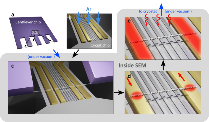
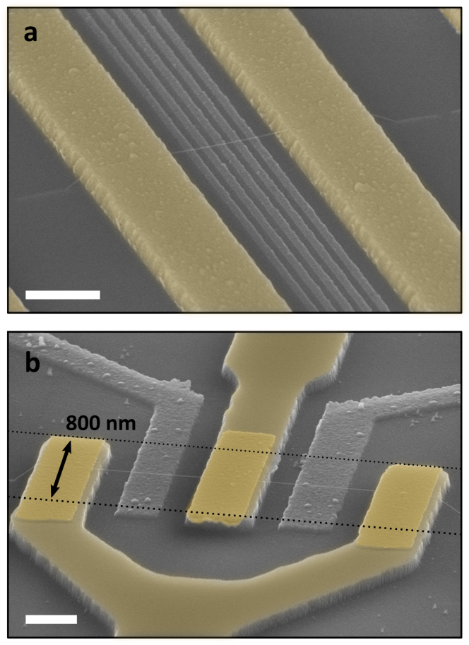
Following the principle of the stamping technique, suspended CNTs are grown between individual cantilevers arranged in an array (see Figure 1.a). In parallel, the circuit chip on which a CNT will be transferred is fabricated using standard lithography techniques (see methods). The full device is then assembled by mechanically transferring a single CNT on top of the circuit (details in methods). In Figure 2, two examples of fabricated circuits with different geometries are presented. One specificity of our approach is to perform the deposition of the CNT inside a dedicated Scanning Electron Microscope (SEM), which presents multiple advantages. First, it allows to localize CNTs on the cantilever chip and transfer a single one onto the circuit while maintaining the CNT and circuit chip under vacuum. Secondly, e-beam imaging combined with a custom piezo-motor stage allowed us to position the CNT on the circuit with a precision of nm (see Figure 2.b). This second point is crucial to realize complex circuits such as SQUIDs (Superconducting QUantum Interference Devices) [33, 34], or charge detectors [18], which require accurate positioning of the CNT. The metal used to contact the CNT is essential to obtain a low resistance CNT-metal interface. Palladium has been shown to be an excellent candidate [35] mainly because of its low workfunction mismatch with CNTs. We thus use palladium as a top layer.
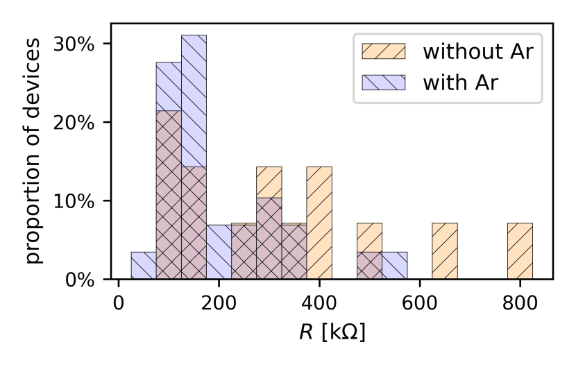
In order to obtain a high quality CNT-metal interface, we paid great attention to the cleanliness of the circuit as well as the CNT throughout the full assembly process. First of all, we remove adsorbates from the surface of the circuit before the transfer of the CNT using an argon-milling process calibrated to etch 5 nm of palladium (see Figure 1.b). Indeed, the first 3-4 nm of palladium can adsorb oxygen [24] which is known to deteriorate the quality of the CNT-metal interface [36, 24, 37]. The resistance improvement due to this pre-cleaning step is quantified in Figure 3. In addition, to maintain a clean surface of the CNT, we developed a transfer technique allowing to maintain the CNT in vacuum from their synthesis to their measurement in a cryostat (mbar during the transfer steps). We believe this strongly reduces the amount of adsorbates at its surface. Finally, because the exposure to the e-beam can induce the deposition of hydrocarbons (see Supplementary Note 2), the region of the circuit where the CNT is transferred onto, is never exposed to the e-beam. For the same reason, the section of the CNT which will be connected is only minimally exposed during localization of the CNT (see Methods).
Current-induced and radiative thermal annealing steps
Nevertheless, having a clean CNT-metal interface is not sufficient to obtain a highly transparent contact, hence we developed a two-step low temperature (below 300 °C) annealing process in which the contact is first improved by driving a large current through the CNT (see Figure 1.a and 1.b) and then further enhanced via RTA (see Figure 1.d and 1.e).
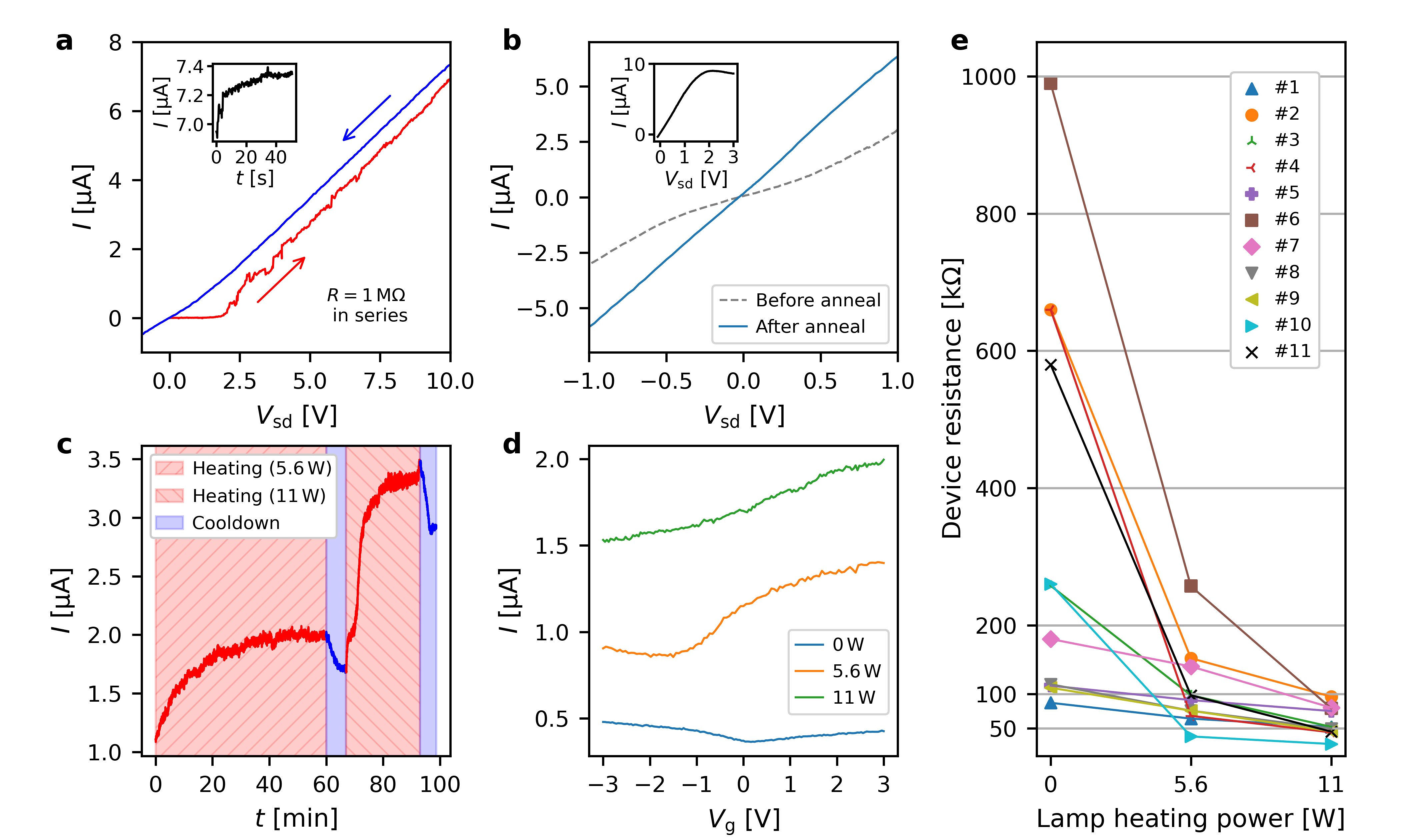
The first current-induced annealing technique is a very local process since most of the heating power is dissipated at the contact between the CNT and the metal (see Figure 1.d). - curves during current-induced annealing are presented in figures 4.a, and 4.b. In order to prevent an accidental cut of the CNT, a first annealing is performed with a resistor in series. On the voltage ramp-up, a current plateau is visible at low bias voltage which is reminiscent of a barrier forming at the CNT-metal interface. It is followed by sudden current jumps suggesting discrete events in the vicinity of the CNT-metal interface, such as atomic rearrangements, or desorption of atoms, which are consistent with the local heating scenario. After this first trace-retrace cycle, the initial current plateau has disappeared, which confirms the decrease of the barrier due to the local events. The CNT junction still displays a weak non-ohmic behavior, which is eliminated by driving the maximum current that the CNT can sustain [38].
The second annealing step consists in a RTA of the entire surface of the device. For this purpose, we use the thermal radiation of a 70W halogen lamp which has been installed inside the SEM vacuum chamber. During the RTA step the device is positioned about 5 mm below the lamp. A tantalum shield partially surrounds the halogen lamp to prevent excessive heating of the SEM column. The RTA is subdivided in two steps, at 5.6 W and 11 W, both ranging from 30 to 60 minutes for most of the devices (see Supplementary Note 6). These power values gave the best result for the different metals used for the bulk of the contact electrodes (Ti, Mo, Nb, see Supplementary Note 6). In contrast to the current-induced annealing, the RTA displays a more continuous evolution of the device resistance (see Figure 4.c and Supplementary Note 4). During the cooldown periods, the resistance increases again which we associate to some thermoelectric effect occurring at metal junctions in the circuit.
The effect of the different annealing steps on the resistance of 11 devices is presented in Figure 4.e. Importantly, one can notice that all devices have a resistance above 50 k after the current-induced annealing, while 7 out of the 11 devices are below this value after the full annealing procedure, showing the substantial effect of RTA. Device 10 could reach a minimal resistance of 25 k. Besides, a resistance of 300 k after the current-induced annealing step strongly helps to reach a final resistance inferior to 50 k. It shows that an initially clean interface is required to reach final low resistance values, underlining the need for an argon-milling pre-treatment step. Moreover, the number of devices for which this behavior has been observed further emphasizes the robustness of our technique.
Another effect of the RTA is to switch the CNT transport behavior from ambipolar to unipolar n-type (see Figure 4.d). This change is accompanied by a shift of the center of the semiconducting gap towards negative gate values. It can be explained either by the modification of the workfunction mismatch between the palladium and the CNT, or by the doping of the CNT [39, 40]. While the exact mechanism taking place in our situation is not clear, both can result from the removal of adsorbates either at the CNT-metal interface or on the CNT itself [41]. In particular, oxygen desorption has been shown to have a dominant effect in similar circuits [39, 40]. Interestingly, the n-type behavior resulting from our approach is in clear opposition to the more common p-type behavior of most CNT-based open quantum circuits realized so far.
It is important to note, that this annealing procedure only requires relatively low temperatures estimated to not exceed 300 °C (see Supplementary Note 3). This temperature has to be compared to the range of 800-900 °C involved in the CNT top-growth fabrication technique [26], as well as the 800 °C needed to form CNT-metal covalent bonds (MoC [25], or TiC formations [42, 43]). We believe RTA is particularly efficient since it directly heats the surface of the circuit which is where the contact between the CNT and the metal is located. This relatively low temperature annealing technique is thus compatible with other quantum technologies such as superconducting circuits (based on Al, Nb, NbTi, …).
Open quantum dot regime
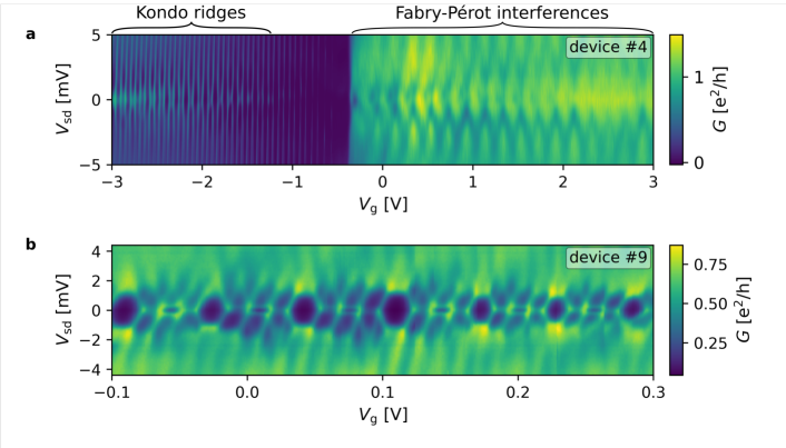
The devices with a resistance below 50 k were further studied with cryogenic transport measurements (see Figure 5 and Supplementary Note 5). In both charge stability diagrams presented in Figure 5, the presence of Kondo-ridges demonstrates that cotunneling processes play a dominant role in the transport spectrum of the device, proving the presence of large tunnel coupling rate between the quantum dot and the Fermi reservoirs [44], but still lower than the charging energy of the quantum dot (). Even higher coupling could be reached as shown by the Fabry-Pérot interference pattern in Figure 5. In this regime, the tunnel coupling rates to the Fermi reservoirs are larger than the charging energy of the quantum dot (), therefore the electron number in the quantum dot is not a good quantum number anymore, proving that it cannot be considered as a closed quantum system. Moreover, the observation of the four-fold degeneracy of the CNT energy levels confirms the very low amount of disorder in the circuit.
Conclusion
To conclude, we demonstrated that the stamping nano-fabrication technique is able to produce CNT-based quantum circuits deep into the open quantum dot regime. For this, we developed a technique relying on the combination of an argon-milling pre-treatment, vacuum transferred CNTs and a two-step annealing procedure, enabling us to reach device resistance values below 50 k. Such low resistance values are sufficient to reach the open quantum dot regime in which cotunneling processes dominate, leading to Kondo physics as well as Fabry-Pérot interferences. Moreover, our technique allows to integrate a CNT into a circuit with a precision of nm. A more meticulous approach combined with dedicated markers should in principle allow to reach a precision down to nm.
The accuracy of this technique, the relatively low required temperature (below 300 °C) and its capability to reach the open quantum regime make it particularly attractive to realize hybrid systems and merge different mature quantum technologies. For instance, one can use a suspended CNT connected with superconducting electrodes to realize a Josephson junction which could be used as the basic element of novel superconducting qubits. The low Josephson energy obtained in nanotube [45] could serve to explore new areas of the parameter space of superconducting qubit [46].
The developed technique is also perfectly suited to realize optomechanics experiments based on CNTs. One promising approach relies on the recently studied flux-mediated phonon-photon coupling [31, 32], for which the large zero-point fluctuations of the CNT are a powerful advantage [30]. Using such a coupling scheme, a single-phonon coupling rate gMHz is within reach (see Supplementary Note 7). This value is sufficient to reach the single photon strong coupling regime allowing to create mechanical quantum state in the CNT such as Schrödinger cat states [47].
Methods
CNT growth
The CNTs are grown using a chemical vapor deposition (CVD) process on a custom cantilever comb chip (see Supplementary Note 1) which allows us to transfer CNTs suspended between cantilevers onto the circuit chips. The growth is performed at 880C for 15 min with precursor gas flows of 75 sccm of CH4 and 50 sccm of H2. We use the same catalyst as in ref [48].
Circuit chip fabrication
The fabrication of the circuit chip comprises four layers of lithography processes on a p-doped SiO2 (300 nm) / Si (500 µm) substrate. First, markers and large structures are patterned with optical lithography and electron-beam evaporation of Ti(3 nm) / Au(40 nm). Gate (Ti/Al/AlOx) and contact electrodes (Ti/electrode material/Pd) are then patterned with electron-beam lithography and electron-beam evaporation with a lift-off process.
In order to transfer a CNT from the cantilever onto the circuit chip, 12 µm deep trenches are patterned with optical lithography and reactive-ion etching using a combination of CHF3/Ar/O2 (SiO2 etching) and SF6/C4F8 (Si etching).
Integration of the CNT
We transfer the cantilever chip from the CVD oven into an SEM with a custom holder using a vacuum transfer arm. The top 60 µm of the cantilever chip are then imaged to preselect the suspended CNT to be stamped (panorama image presented in Supplementary Figure S1). Prior to stamping, the surface of the circuit chip is cleaned with an argon-milling process using a Kaufman source (for 90 s, at a discharge voltage of 40 V, with a flow of 9 sccm Ar and a beam acceleration voltage of 200 V). This removes about 5 nm of Pd including the oxygen adsorbed at the surface [24].
The circuit chip is then micro-bonded and transferred into the SEM usually within 15-20 min. Because oxygen diffusion at the Pd surface takes place over several hours [24], we believe the short exposure time to air of 15-20 min after argon-milling is not detrimental to the quality of the surface. The cantilever pair with the preselected suspended CNT is laterally aligned with the stamping position on the sample chip using piezomotors (minimum step size: 10 nm). The cantilevers are then lowered into the trenches of the circuit chip while tracking the distance between the CNT and the surface of the circuit with the SEM. Electron-beam exposure of the whole tube is limited to the quick overview panorama image (see Supplementary Note 1). During the approach only few microns of the tube edge are exposed to the e-beam while the central part remains unexposed. We apply a bias of 4 V between the two outermost electrodes and the next inner electrodes and once the CNT is in mechanical contact a current through it is measured showing that it has been contacted electrically. To retract the cantilever chip without affecting the CNT segment of interest, the circuit chip contains dedicated cutting sections where the CNT junction can be cut by driving a high current (10 µA) through the CNT. After annealing the individual junctions by driving a high current through the CNT, the chip is radiatively heated with the halogen lamp. Circuit chips with CNT junctions of resistance below 50 k at a bias of 0.1 V are then vacuum-transferred to a dilution cryostat with 30 mK base temperature where the low-temperature measurements are performed. During the whole process, the CNTs are thus never exposed to air.
Acknowledgement
We thank the KIT Nanostructure Service Laboratory (NSL) for the technical support in the nanofabrication of the devices. T.A. acknowledges financial support from the Hector Fellow Academy. All authors acknowledge support from the Leibniz award WE 4458-5, and the DFG grant WE 4458/2-1.
Data availability
The data that support the findings of this study are available from the corresponding author upon reasonable request.
Author contributions
T.A, T.C, and A.A performed the measurements. T.A and T.C fabricated the devices with the help of A.A. T.A performed the data analysis with the assistance of T.C and A.A. T.A and T.C developed the nano-assembly method with the help of A.A, C.S, and W.W. T.C developed the experimental setup with the help of T.A, A.A, C.S, and W.W. T.C wrote the manuscript, and T.A wrote the supplementary materials. A.A and W.W proofread the manuscript and the supplementary materials.
Competing interests
The authors declare no competing interests.
References
- [1] Vikram V Deshpande and Marc Bockrath “The one-dimensional Wigner crystal in carbon nanotubes” In Nature Physics 4.4 Nature Publishing Group UK London, 2008, pp. 314–318
- [2] Sharon Pecker et al. “Observation and spectroscopy of a two-electron Wigner molecule in an ultraclean carbon nanotube” In Nature Physics 9.9 Nature Publishing Group UK London, 2013, pp. 576–581
- [3] I Shapir et al. “Imaging the electronic Wigner crystal in one dimension” In Science 364.6443 American Association for the Advancement of Science, 2019, pp. 870–875
- [4] E A Laird, F Pei and L P Kouwenhoven “A valley–spin qubit in a carbon nanotube” In Nature nanotechnology 8.8 Nature Publishing Group UK London, 2013, pp. 565–568
- [5] T Cubaynes et al. “Highly coherent spin states in carbon nanotubes coupled to cavity photons” In npj Quantum Information 5.1 Nature Publishing Group UK London, 2019, pp. 47
- [6] B Lassagne et al. “Coupling mechanics to charge transport in carbon nanotube mechanical resonators” In Science 325.5944 American Association for the Advancement of Science, 2009, pp. 1107–1110
- [7] G A Steele et al. “Strong coupling between single-electron tunneling and nanomechanical motion” In Science 325.5944 American Association for the Advancement of Science, 2009, pp. 1103–1107
- [8] N Ares et al. “Sensitive radio-frequency measurements of a quantum dot by tuning to perfect impedance matching” In Physical Review Applied 5.3 APS, 2016, pp. 034011
- [9] Carlos Urgell et al. “Cooling and self-oscillation in a nanotube electromechanical resonator” In Nature Physics 16.1 Nature Publishing Group UK London, 2020, pp. 32–37
- [10] Yutian Wen et al. “A coherent nanomechanical oscillator driven by single-electron tunnelling” In Nature physics 16.1 Nature Publishing Group UK London, 2020, pp. 75–82
- [11] J Waissman et al. “Realization of pristine and locally tunable one-dimensional electron systems in carbon nanotubes” In Nature nanotechnology 8.8 Nature Publishing Group UK London, 2013, pp. 569–574
- [12] C C Wu, C H Liu and Z Zhong “One-step direct transfer of pristine single-walled carbon nanotubes for functional nanoelectronics” In Nano letters 10.3 ACS Publications, 2010, pp. 1032–1036
- [13] M Muoth and C Hierold “Transfer of carbon nanotubes onto microactuators for hysteresis-free transistors at low thermal budget” In 2012 IEEE 25th International Conference on Micro Electro Mechanical Systems (MEMS), 2012, pp. 1352–1355 IEEE
- [14] F Pei, Edward A L, G A Steele and L P Kouwenhoven “Valley–spin blockade and spin resonance in carbon nanotubes” In Nature nanotechnology 7.10 Nature Publishing Group UK London, 2012, pp. 630–634
- [15] Stefan Blien et al. “Quartz Tuning-Fork Based Carbon Nanotube Transfer into Quantum Device Geometries” In physica status solidi (b) 255.12 Wiley Online Library, 2018, pp. 1800118
- [16] Jörg Gramich et al. “Fork stamping of pristine carbon nanotubes onto ferromagnetic contacts for spin-valve devices” In physica status solidi (b) 252.11 Wiley Online Library, 2015, pp. 2496–2502
- [17] T Cubaynes et al. “Nanoassembly technique of carbon nanotubes for hybrid circuit-QED” In Applied Physics Letters 117.11 AIP Publishing LLC, 2020, pp. 114001
- [18] J Waissman “Carbon Nanotubes for the Generation and Imaging of Interacting 1D States of Matter” Harvard University, 2014
- [19] V Ranjan et al. “Clean carbon nanotubes coupled to superconducting impedance-matching circuits” In Nature communications 6.1 Nature Publishing Group UK London, 2015, pp. 7165
- [20] Stefan Blien et al. “Quantum capacitance mediated carbon nanotube optomechanics” In Nature Communications 11.1 Nature Publishing Group UK London, 2020, pp. 1636
- [21] Yunsung Woo, Georg S Duesberg and Siegmar Roth “Reduced contact resistance between an individual single-walled carbon nanotube and a metal electrode by a local point annealing” In Nanotechnology 18.9 IOP Publishing, 2007, pp. 095203
- [22] Hideyuki Maki, Masaki Suzuki and Koji Ishibashi “Local change of carbon nanotube-metal contacts by current flow through electrodes” In Japanese journal of applied physics 43.4S IOP Publishing, 2004, pp. 2027
- [23] Wei Yang et al. “Fabry-Pérot oscillations in correlated carbon nanotubes” In Physical Review Letters 125.18 APS, 2020, pp. 187701
- [24] S Jung et al. “Understanding and improving carbon nanotube-electrode contact in bottom-contacted nanotube gas sensors” In Sensors and Actuators B: Chemical 331 Elsevier, 2021, pp. 129406
- [25] Qing Cao et al. “End-bonded contacts for carbon nanotube transistors with low, size-independent resistance” In Science 350.6256 American Association for the Advancement of Science, 2015, pp. 68–72
- [26] J Cao, Q Wang and H Dai “Electron transport in very clean, as-grown suspended carbon nanotubes” In Nature materials 4.10 Nature Publishing Group UK London, 2005, pp. 745–749
- [27] Alexander Eichler et al. “Nonlinear damping in mechanical resonators made from carbon nanotubes and graphene” In Nature nanotechnology 6.6 Nature Publishing Group UK London, 2011, pp. 339–342
- [28] R Tormo-Queralt et al. “Novel Nanotube Multiquantum Dot Devices” In Nano Letters 22.21 ACS Publications, 2022, pp. 8541–8549
- [29] Jing Kong et al. “Synthesis of individual single-walled carbon nanotubes on patterned silicon wafers” In Nature 395.6705 Nature Publishing Group UK London, 1998, pp. 878–881
- [30] K E Khosla, M R Vanner, N Ares and E A Laird “Displacemon electromechanics: how to detect quantum interference in a nanomechanical resonator” In Physical Review X 8.2 APS, 2018, pp. 021052
- [31] IC Rodrigues, D Bothner and GA Steele “Coupling microwave photons to a mechanical resonator using quantum interference” In Nature communications 10.1 Nature Publishing Group UK London, 2019, pp. 5359
- [32] P Schmidt et al. “Sideband-resolved resonator electromechanics based on a nonlinear Josephson inductance probed on the single-photon level” In Communications Physics 3.1 Nature Publishing Group UK London, 2020, pp. 233
- [33] J-P Cleuziou et al. “Carbon nanotube superconducting quantum interference device” In Nature nanotechnology 1.1 Nature Publishing Group UK London, 2006, pp. 53–59
- [34] BH Schneider, S Etaki, HSJ Van Der Zant and GA Steele “Coupling carbon nanotube mechanics to a superconducting circuit” In Scientific reports 2.1 Nature Publishing Group UK London, 2012, pp. 599
- [35] A Javey et al. “Ballistic carbon nanotube field-effect transistors” In nature 424.6949 Nature Publishing Group UK London, 2003, pp. 654–657
- [36] A Felten et al. “The role of oxygen at the interface between titanium and carbon nanotubes” In ChemPhysChem 10.11 Wiley Online Library, 2009, pp. 1799–1804
- [37] P G Collins, K Bradley, M Ishigami and d A Zettl “Extreme oxygen sensitivity of electronic properties of carbon nanotubes” In science 287.5459 American Association for the Advancement of Science, 2000, pp. 1801–1804
- [38] E Pop et al. “Negative differential conductance and hot phonons in suspended nanotube molecular wires” In Physical Review Letters 95.15 APS, 2005, pp. 155505
- [39] V Derycke, R Martel, J Appenzeller and Ph Avouris “Carbon nanotube inter-and intramolecular logic gates” In Nano letters 1.9 ACS Publications, 2001, pp. 453–456
- [40] V Derycke, R Martel, J Appenzeller and Ph Avouris “Controlling doping and carrier injection in carbon nanotube transistors” In Applied Physics Letters 80.15 American Institute of Physics, 2002, pp. 2773–2775
- [41] YF Chen and M S Fuhrer “Tuning from thermionic emission to ohmic tunnel contacts via doping in Schottky-barrier nanotube transistors” In Nano letters 6.9 ACS Publications, 2006, pp. 2158–2162
- [42] R Martel et al. “Ambipolar electrical transport in semiconducting single-wall carbon nanotubes” In Physical review letters 87.25 APS, 2001, pp. 256805
- [43] Y Zhang et al. “Heterostructures of single-walled carbon nanotubes and carbide nanorods” In Science 285.5434 American Association for the Advancement of Science, 1999, pp. 1719–1722
- [44] Jesper Nygård, David Henry Cobden and Poul Erik Lindelof “Kondo physics in carbon nanotubes” In Nature 408.6810 Nature Publishing Group UK London, 2000, pp. 342–346
- [45] Matthias Mergenthaler et al. “Circuit quantum electrodynamics with carbon-nanotube-based superconducting quantum circuits” In Physical Review Applied 15.6 APS, 2021, pp. 064050
- [46] Ivan V Pechenezhskiy et al. “The superconducting quasicharge qubit” In Nature 585.7825 Nature Publishing Group UK London, 2020, pp. 368–371
- [47] Bradley D Hauer, Joshua Combes and John D Teufel “Nonlinear Sideband Cooling to a Schr” odinger Cat State of Motion” In arXiv preprint arXiv:2208.02371, 2022
- [48] JJ Viennot, J Palomo and T Kontos “Stamping single wall nanotubes for circuit quantum electrodynamics” In Applied Physics Letters 104.11 American Institute of Physics, 2014, pp. 113108