Tensile strain induced brightening of momentum forbidden dark exciton in WS2
Abstract
Transition-metal dichalcogenides (TMDs) host tightly bound quasi-particles called excitons. Based on spin and momentum selection rules, these excitons can be either optically bright or dark. In tungsten-based TMDs, momentum-forbidden dark exciton is the energy ground state and therefore it strongly affect the emission properties. In this work, we brighten the momentum forbidden dark exciton by placing WS2 on top of nanotextured substrates which put the WS2 layer under tensile strain, modifying electronic bandstructure. This enables phonon assisted scattering of exciton between momentum valleys, thereby brightening momentum forbidden dark excitons. Our results will pave the way to design ultrasensitive strain sensing devices based on TMDs.
TMDs (e.g. , , W, , Se) are known for their novel optical properties[1, 2, 3, 4]. They host excitons - charge neutral electron-hole pairs bound by Coulomb interactions.[5, 6]. The large spin-orbit coupling in WS2 due to the heavy mass of W atom, splits the valance band (VB) maxima and conduction band (CB) minima at , points in two sub-bands with opposite spin orientations (up, down at and down, up at ) respectively. This results in the formation of two ‘bright’ intravalley excitons with opposite spins at , [7]. There is possibility for the formation of indirect intervalley excitons as well. But because of the large momentum mismatch, they require the assistance of phonons to recombine radiatively by emitting a photon[8]. The exciton is therefore called momentum-forbidden dark exciton. In case of W-based ML TMDs, exciton is the excitonic ground state and has higher binding energy and longer lifetime than the bright excitons , and therefore they play an important role in the exciton dynamics of the system[9, 10]. Thus, controlling them is essential for designing novel optical devices. The dark exciton can be brightened by exciton-phonon coupling if the energy of the available phonon mode matches with the dark-bright exciton energy splitting which can be effectively tuned by applying strain on ML WS2[11, 9, 12]. Therefore, strain acts as a tuning knob for the emission of dark excitons[13, 9].
In this work, we apply tensile strain on ML WS2 by placing them on nanotextured substrates patterened with nanopillars. The nanopillars of height ‘h’ and interpillar seperation (center to center) ‘l’ [Fig.1a, c]. Conically shaped nanopillars made of Si(100) have insulator Al2O3 nanospheres 10 nm on top[Fig.1c].
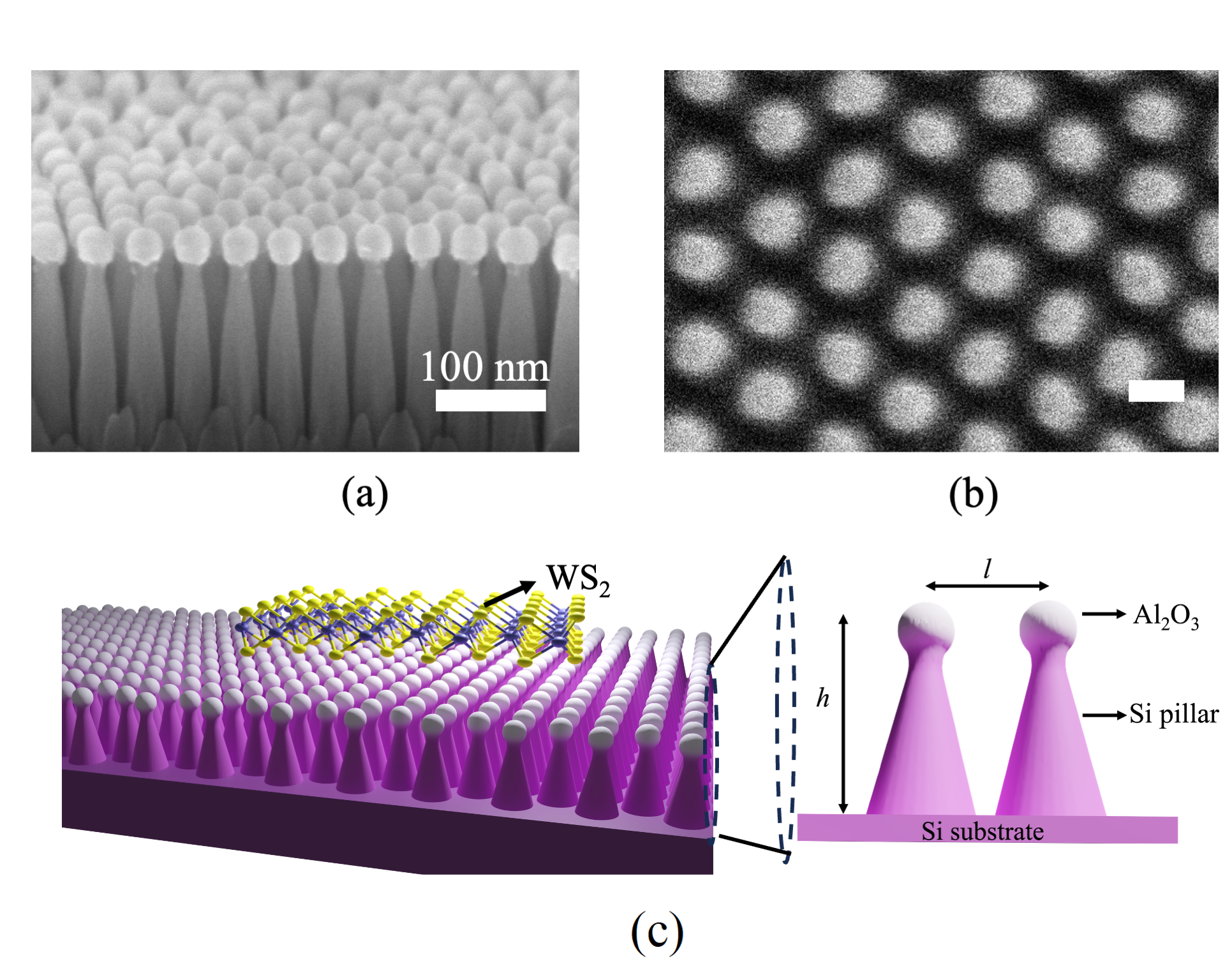
We prepared samples with varied interpillar distances: l 25 nm(sample C-49), l 44 nm (C-99) and l 60nm (C-132). By tuning ‘l’ we tune the amount of strain applied on ML-WS2. ML WS2 was grown by chemical vapour deposition (CVD) and was transferred on top of the nanotextured substrate by wet transfer technique [Fig. 1b] (details of sample preparation and characterization can be found in supplemental material section I, XI and our previous work[14, 15]). We perform temperature dependent photoluminescence (PL) and Raman measurements on the strained and unstrained ML WS2 samples. Supported by, ab initio calculations, we discover the brightening of K dark excitons by applying tensile strain.
The PL measurements were performed using a continuous wave laser of wavelength 514.5 nm. The details of the measurement can be found in the supplemental material section II. In the temperature dependent PL study of ML WS2 on C-99 substrate [Fig. 2a], two well resolved peaks, one at 2.01 eV (FWHM 24 meV) and other at 1.95 eV (FWHM 32 meV) were observed at 280 K. The peak position and FWHM were extracted from each PL spectrum by fitting with a sum of Gaussian functions (see supplemental material section VI for details). We attribute the peak at 2.01 eV as bright exciton peak (X0) and the peak at 1.95 eV as negatively charged trion peak (X-) since ML WS2 is a n-doped semiconductor.We further confirm this attribution of peaks from excitation power (P) dependence of the integrated intensity (I). The data were fitted with the power law dependence I Pα and we obtained values for of 0.9, 1.03 for X0 and X- respectively, typical for excitons and trions (see supplemental material section VII)[16, 17, 18]. As we lower the temperature both X0, X- blueshift as reported earlier[18]. At around 200 K a new peak starts to appear at 1.94 eV. As we further decrease the temperature, the intensity of new peak increases while the opposite is true for X- and X0: their intensity diminish[19]. The new peak can be attributed to (a) a biexciton, XX (b) a defect bound exciton (XL) or (c) a dark exciton (XD). The exponent of the power law dependence for XX and XL is known to be superlinear (2.0) and sublinear (0.5) respectively[16, 17, 18]. From the I vs P plot of the new peak we obtain a value of of about 0.97 and 1.15 at 180 and 100 K respectively (see Fig. 2d and supplemental material section VII). Moreover, the new peak do not show any blueshift with increasing excitation power, characteristic of XL because of its broad energy distribution [20, 21]. However, it showed red shift due to local heating, a behaviour generally seen in excitons [14] (see supplemental material section VIII). Furthermore, the new peak also shows anisotropy in circular polarization dependent PL, uncharacteristic of XL [22, 21](see supplemental information section IV for details). Therefore, the new peak is neither XX or XL. However, value of and its peak position at 77 K eV is similar to recent reports of observation of dark exciton under strain and strong exciton-phonon coupling[23]. We therefore attribute this new peak at eV as XD. We performed the similar study on other two samples namely C-48 and C-132 [Fig. 2b and c]. For the C-48 and C-132 samples we observed X0 and X- peaks at room temperature but no new peaks were observed as we lowered the temperature to 77 K. The X0 and X- showed blueshift and narrowing with decreasing temperature similar to that of C-99 sample.
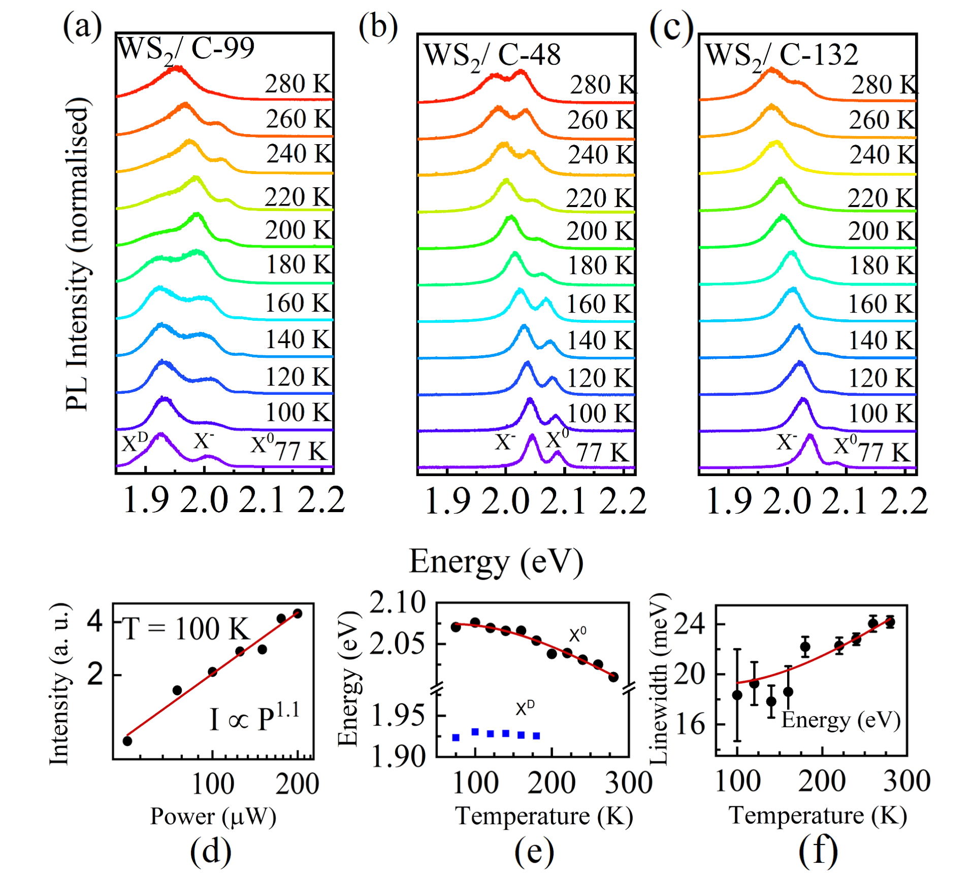
The temperature dependence of the peak position of X0 in C-99 sample was studied in detail [Fig. 2e]. The temperature dependence shows a characteristic redshift with decreasing temperature induced by a exciton-phonon coupling. This can be described by the phenomenological model proposed by O’Donnell and Chen[24]:
| (1) |
where E(T) is the resonance energy of X0 at temperature T, S is dimensionless exciton-phonon coupling constant, is Boltzmann constant and is the average phonon energy responsible for the coupling. By fitting the experimental data we obtained the parameters, E(0)= 2.074 0.003 eV, S= 3.65 0.98 and = 43 10 meV. The value of is close to the energy of E phonon ( 43.9 meV) mode of ML WS2. This suggests that the E phonon mode has a crucial role in the exciton-phonon coupling. Note that the peak position of XD changes only by 2 meV as we increase the temperature from 75 K to 180 K, whereas, in the same temperature range the X0 peak position changes by 20 meV. This observation is consistent with the fact that the CB minima at K point shifts at a much faster rate with temperature compared to the point [23]. To determine the strength of exciton-phonon coupling, the evolution of the FWHM of X0 was fitted by a phonon-induced broadening model[Fig. 2f][25, 26]:
| (2) |
where is the intrinsic FWHM, the linear term in T is due to the interaction of acoustic phonon modes (LA and TA) and the last term is the interaction term with the optical phonon mode[27]. c2 is the measure of the exciton- optical phonon coupling strength. The value of that we obtained previously by fitting Eq. 1, was used for fitting Eq. 2. The value of c2 obtained by fitting Eq. 2 is 26.5 4.6 and is significantly higher than the previously reported value of 6.5 for ML WS2[26]. This higher value of c2 further confirms the strong exciton and E phonon mode coupling in C-99 substrate. See supplemental material section XII. for the above analysis of XD peak in ML WS2 on top of C-48 and C-132 substrate.
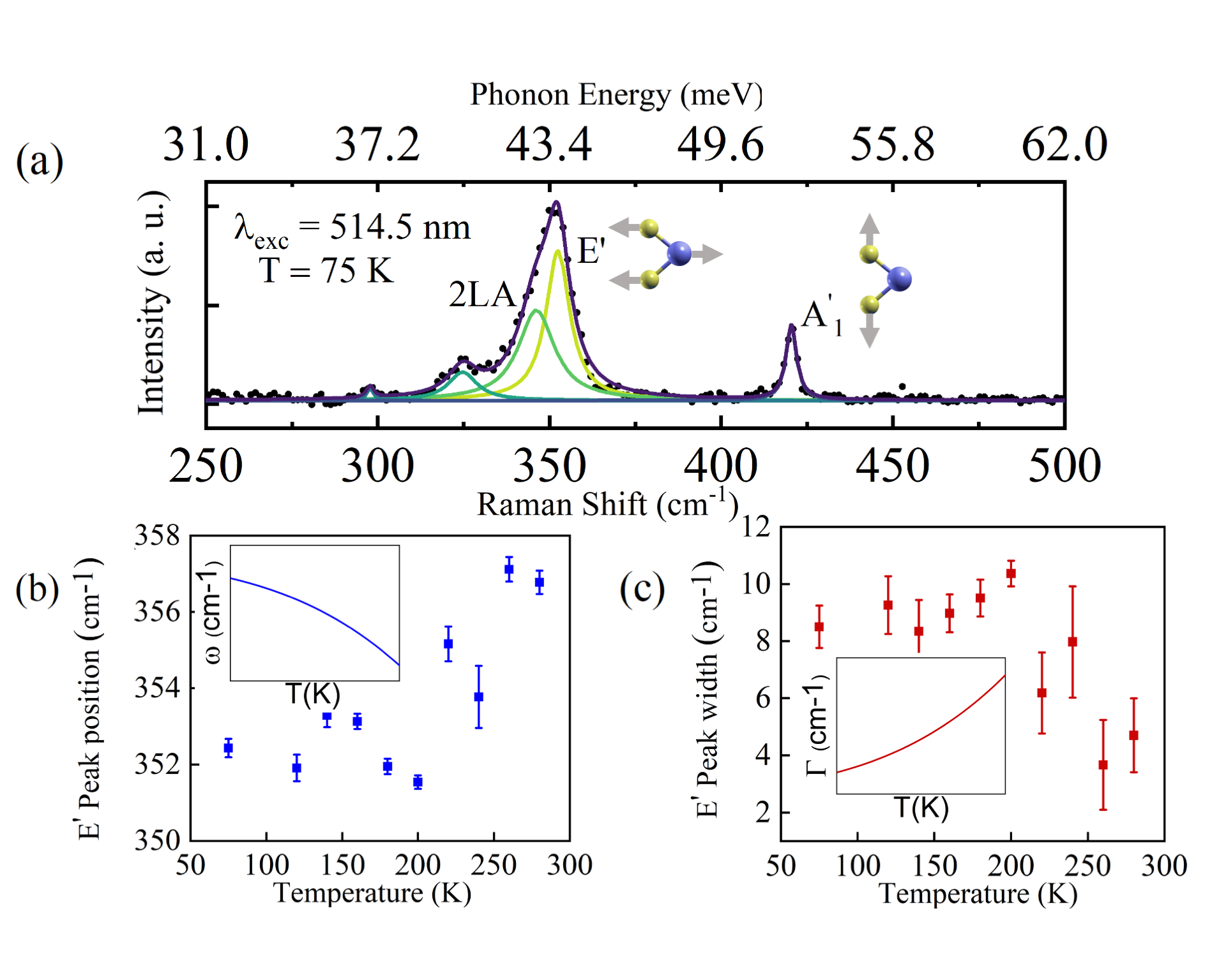
We further did temperature dependent Raman study on the C-99 sample. Phonon modes responsible for electron-phonon scattering in case of ML WS2 are LA, TA, E and A1 modes[28]. The various Raman peaks (E, 2LA, A) were analysed with multiple Lorentzian functions[ Fig. 3a][29] (see supplemental material section IX for fitting details). All the phonon modes except the in-plane E mode showed redshift in Raman shift and an increase in their linewidth with increasing temperature [see Fig. 3b, c for E and supplemental material section X for A]. The redshift and increasing linewidth with temperature can be explained by anharmonic cubic equations[30, 31]:
| (3) |
| (4) |
where , are the frequency of the phonon mode and linewidth at temperature T respectively. , are the frequency of phonon mode and linewidth at T= 0 K respectively and C is a constant. The behaviour of Eq. 3 and Eq. 4 as a function of temperature is plotted in the insets of Fig. 3b and c. The E phonon modes shows a completely opposite trend when compared to Eq. 3 and Eq. 4 [Fig. 3b, c]. This anomalous behaviour of E phonon mode is related to strong electron-phonon coupling[32, 33, 34]. The various factors affecting the Raman mode frequency can be expressed mathematically as [35] where corresponds to quasiharmonic contribution due to change in unit-cell volume, corresponds to phonon-phonon interaction related anharmonic effects, is due to spin-phonon coupling and is due to electron-phonon coupling. Eq. 3 and 4 take into account the first three terms but not the last term. Therefore Eq. 3 and 4 fails to describe the anomalous behaviour of the E Raman modes.
To understand the effect of strain, calculated the electronic band structure of ML-WS2 by DFT using full-relativistic ultrasoft pseudopotential with Perdew–Burke–Ernzerhof (PBE) exchange-correlation functionals alongside plane waves implemented in Quantum ESPRESSO package [Fig.4a] (see supplemental material section V for details). With increasing tensile(compressive) strain the absolute CB minima at K- point shifts down (up) and the local CB minima at shifts up (down). The VB maxima at K and shows almost no change with strain[Fig. 4a]. We denote the direct bandgap at K point as EKK and the indirect bandgap at point as EKΛ. Note that, in electronic band structure the CB minima at point is at higher energy than the CB minima at K point by EKΛ - EKK = = 64 meV. To get into the exciton picture from electron-hole picture (as described in ref. [9, 7]) we need to calculate the binding energy of the excitons. The binding energy (Eb) is calculated from the effective mass model [36]:
| (5) |
where the exciton reduced mass, mh and me are the effective masses of holes and electrons respectively (see supplemental material section XIV for details). is the dielectric constant of ML WS2, e is the electron charge and n is the principal quantum number. me and mh are calculated from parabolic band approximation of the electronic bands obtained from DFT calculations (extracted values are listed in Table 1)[37]. of ML-WS2 was taken to be 5 for n as was shown in [36]. of K-K exciton (X0) and K- exciton (XD) are 0.155m0 and 0.219m0 respectively, where m0 is the free electron mass. Using Eq. 5 we found Eb of X0 and XD 310 meV and 438 meV respectively. Now, if we visualize the scenario in the excitonic picture, the K-K bright exciton state is formed at the point (zero momentum point) in the center of mass (COM) coordinates at the position E = EKK - E and the K- dark exciton state is formed at the point in COM coordinates at the position E = EKΛ - E[38]. As the E is higher than E, XD is at a lower energy than X0 in the exciton picture, unlike the electron-hole picture. Our calculations show that, in unstrained sample, the dark state is below the bright state by energy E - E = E meV. Under strain, the excitonic states at (COM) and (COM) points behave similar to the CB minima at K and point respectively. The change of E as a function of strain is plotted in Fig. 4c (the values used to generate this plot can be found in supplementary section V). The fitting shows 184 2.5 meV change of E with 1% of applied strain. Note that Eb does not change that much with strain as the latter has little influence on [39, 9].
| m | m | m | ||
|---|---|---|---|---|
| 0.272 m0 | 0.358 m0 | 0.563 m0 | 0.155 m0 | 0.219 m0 |
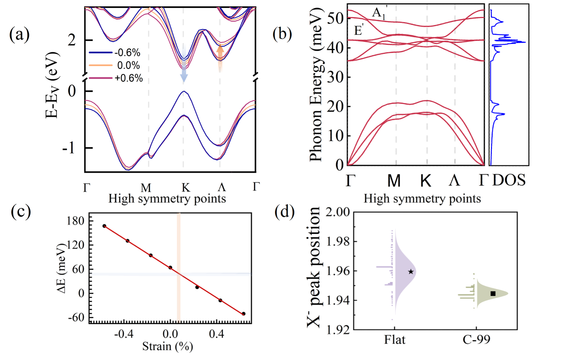
On optically exciting a coherent exciton population at point (COM), K-K bright excitons are formed. Incoherent excitons are then formed at point (COM) by phonon assisted scattering of excitons from point (COM), where a phonon covers the energy and momentum mismatch[11]. However, in the unstrained case, no optical or acoustic phonon modes with energy E 64 meV are available, therefore K- states are not formed at point (COM). Whenever we apply tensile strain on the ML WS2, E decreases and under 0.11 0.01% strain the value of E is 44 meV. From the PL map (see supplemental material section XIII) of X- and X0 the distribution of their positions was plotted. The statistical distribution was fitted with a normal distribution to extract the mean and standard deviation [Fig. 4d]. To estimate the amount of strain on ML WS2 on top of C-99 substrate due to nanopillars, its position of X- was compared with the X- position in ML WS2 on top of flat SiO2/Si [Fig. 4d]. ML WS2 on top of flat SiO2/Si was considered to be unstrained. We did not take into account X0 position for this purpose because X0 was not clearly resolved in ML WS2 on top of flat SiO2/Si. The mean X- position was found to be 1.96 eV and 1.94 eV for SiO2/Si and C-99 respectively. This amounts to 20 meV redshift of X- in C-99. It is reported that X- and X0 redhshifts by 130 and 127 meV respectively for 1% applied tensile strain[40]. Therefore we can estimate that ML WS2 on top of C-99 is under a tensile strain of 0.15 %. In C-99 sample phonon assisted scattering of excitons from point (COM) to valley (COM) is possible, thereby forming a population of K- excitonic states in the point (COM). The scattering process is illustrated in the schematic Fig. 5a. An E phonon with momentum (since at point (COM) momentum is zero) and energy 44 meV can make this scattering possible. The calculated phonon density of states shows a large number of phonon states available at 44 meV, thereby making this scattering more favorable [Fig. 4b]. Note that, change of phonon energy with strain is very negligible[41]. The K- states at point (COM) then can scatter non-radiatively to a virtual state inside the light cone at point (COM) by emitting phonons. Once inside the light cone, the ‘dark’ excitons can decay radiatively from the virtual state by emitting photon, thus leaving its signature in the PL spectra.
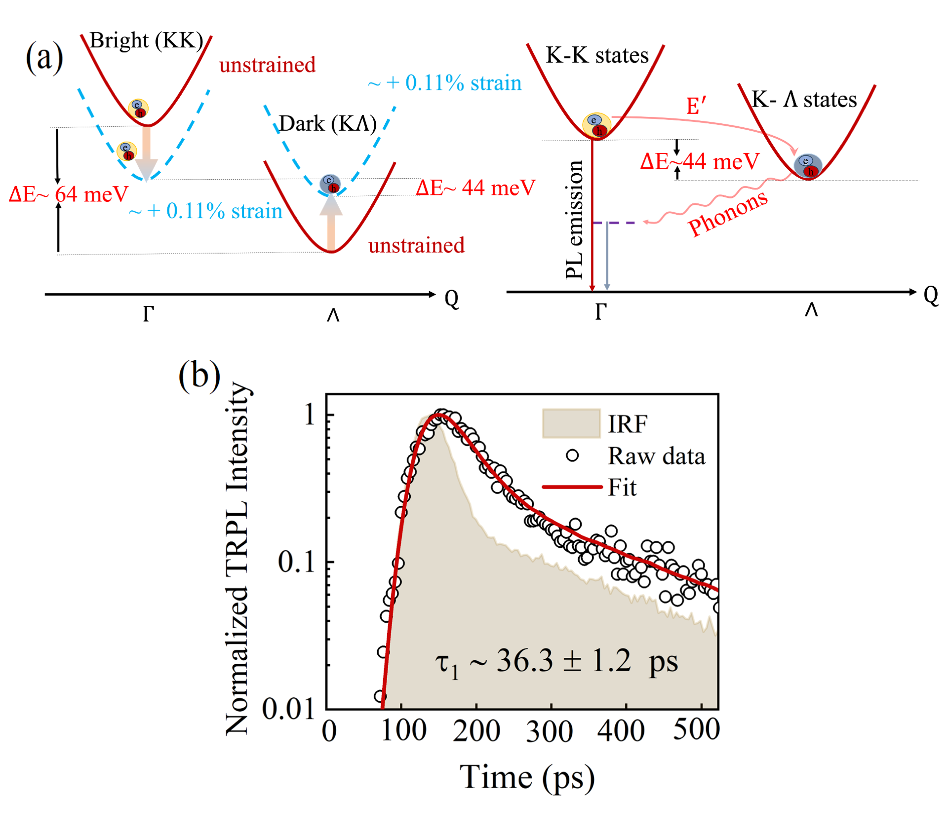
To know about the kinetics of XD, we did time-resolved PL (TRPL) on the ML WS2 on top of C-99 substrate (see measurement details in supplemental material section III). The measured TRPL data was fitted with two exponentials () after deconvoluting from the IRF as implemented in QuCoa software (PicoQuant)[Fig.5b]. The faster and stronger component which represents the XD decay time is estimated to be 36.3 1.2 ps. This value of is 30 times larger than the reported decay time of a neutral exciton X0 ( 1 ps at T = 60 K) in literature [42, 43] . This longer lifetime of XD compared to X0 is expected because, XD is excitonic ground state of ML WS2[23, 10]. The slower () and weak decay component 100 ps is expected to be coming from the contribution of tail of defect-bound exciton complex observed in ML WS2 at lower temperatures[44].
In summary, we have reported the experimental observation of momentum-forbidden K- dark excitons by applying tensile strain on ML WS2 using a nanotextured substrate. The 2D TMDs are known to buckle easily with compressive strain[45] and is also more difficult to create, especially at low temperatures which is essential to prevent thermally activated depopulation of dark state into the bright state. However, it’s easy to create tensile strain in the 2D TMDs and they can endure high values of tensile strength as well . Therefore it would be more practical and application-oriented if we can modulate the dark exciton with tensile strain rather than compressive strain.
References
- Novoselov et al. [2005] K. S. Novoselov, D. Jiang, F. Schedin, T. Booth, V. Khotkevich, S. Morozov, and A. K. Geim, Proc. Natl. Acad. Sci. U.S.A. 102, 10451 (2005).
- Britnell et al. [2013] L. Britnell, R. M. Ribeiro, A. Eckmann, R. Jalil, B. D. Belle, A. Mishchenko, Y.-J. Kim, R. V. Gorbachev, T. Georgiou, S. V. Morozov, A. N. Grigorenko, A. K. Geim, C. Casiraghi, A. H. C. Neto, and K. S. Novoselov, Science 340, 1311 (2013).
- Mak et al. [2010] K. F. Mak, C. Lee, J. Hone, J. Shan, and T. F. Heinz, Phys. Rev. Lett. 105, 136805 (2010).
- Ross et al. [2013] J. S. Ross, S. Wu, H. Yu, N. J. Ghimire, A. M. Jones, G. Aivazian, J. Yan, D. G. Mandrus, D. Xiao, W. Yao, and X. Xu, Nat. Commun. 4, 1474 (2013).
- Splendiani et al. [2010] A. Splendiani, L. Sun, Y. Zhang, T. Li, J. Kim, C.-Y. Chim, G. Galli, and F. Wang, Nano Lett. 10, 1271 (2010).
- He et al. [2014] K. He, N. Kumar, L. Zhao, Z. Wang, K. F. Mak, H. Zhao, and J. Shan, Phys. Rev. Lett. 113, 026803 (2014).
- Malic et al. [2018] E. Malic, M. Selig, M. Feierabend, S. Brem, D. Christiansen, F. Wendler, A. Knorr, and G. Berghäuser, Phys. Rev. Mater. 2, 014002 (2018).
- Brem et al. [2020] S. Brem, A. Ekman, D. Christiansen, F. Katsch, M. Selig, C. Robert, X. Marie, B. Urbaszek, A. Knorr, and E. Malic, Nano Lett. 20, 2849 (2020).
- Feierabend et al. [2019] M. Feierabend, Z. Khatibi, G. Berghäuser, and E. Malic, Phys. Rev. B 99, 195454 (2019).
- Madéo et al. [2020] J. Madéo, M. K. L. Man, C. Sahoo, M. Campbell, V. Pareek, E. L. Wong, A. Al-Mahboob, N. S. Chan, A. Karmakar, B. M. K. Mariserla, X. Li, T. F. Heinz, T. Cao, and K. M. Dani, Science 370, 1199 (2020).
- Selig et al. [2018] M. Selig, G. Berghäuser, M. Richter, R. Bratschitsch, A. Knorr, and E. Malic, 2D Mater. 5, 035017 (2018).
- Zollner et al. [2019] K. Zollner, P. E. F. Junior, and J. Fabian, Phys. Rev. B 100, 195126 (2019).
- Niehues et al. [2018] I. Niehues, R. Schmidt, M. Drüppel, P. Marauhn, D. Christiansen, M. Selig, G. Berghäuser, D. Wigger, R. Schneider, L. Braasch, R. Koch, A. Castellanos-Gomez, T. Kuhn, A. Knorr, E. Malic, M. Rohlfing, S. Michaelis de Vasconcellos, and R. Bratschitsch, Nano Lett. 18, 1751 (2018).
- Chowdhury et al. [2021] T. Chowdhury, D. Paul, D. Nechiyil, G. M. A, K. Watanabe, T. Taniguchi, G. V. P. Kumar, and A. Rahman, 2D Mater. 8, 045032 (2021).
- Rahman et al. [2015] A. Rahman, A. Ashraf, H. Xin, X. Tong, P. Sutter, M. D. Eisaman, and C. T. Black, Nat. Commun. 6, 5963 (2015).
- Shang et al. [2015] J. Shang, X. Shen, C. Cong, N. Peimyoo, B. Cao, M. Eginligil, and T. Yu, ACS Nano 9, 647 (2015).
- Paradisanos et al. [2017] I. Paradisanos, S. Germanis, N. Pelekanos, C. Fotakis, E. Kymakis, G. Kioseoglou, and E. Stratakis, Appl. Phys. Lett. 110 (2017).
- Plechinger et al. [2015] G. Plechinger, P. Nagler, J. Kraus, N. Paradiso, C. Strunk, C. Schüller, and T. Korn, Phys. Status Solidi (RRL) 9, 457 (2015).
- Feierabend et al. [2017a] M. Feierabend, G. Berghäuser, A. Knorr, and E. Malic, Nature Communications 8, 14776 (2017a).
- Kaupmees et al. [2020] R. Kaupmees, M. Grossberg, M. Ney, A. Asaithambi, A. Lorke, and J. Krustok, physica status solidi (RRL) – Rapid Research Letters 14, 1900355 (2020).
- Saigal and Ghosh [2015] N. Saigal and S. Ghosh, Applied Physics Letters 107, 242103 (2015).
- Saigal and Ghosh [2016] N. Saigal and S. Ghosh, Applied Physics Letters 109, 122105 (2016).
- Chand et al. [2022] S. B. Chand, J. M. Woods, E. Mejia, T. Taniguchi, K. Watanabe, and G. Grosso, Nano Lett. 22, 3087 (2022).
- O’donnell and Chen [1991] K. P. O’donnell and X. Chen, Appl. Phys. Lett. 58, 2924 (1991).
- Selig et al. [2016] M. Selig, G. Berghäuser, A. Raja, P. Nagler, C. Schüller, T. F. Heinz, T. Korn, A. Chernikov, E. Malic, and A. Knorr, Nat. Commun. 7, 13279 (2016).
- Cadiz et al. [2017] F. Cadiz, E. Courtade, C. Robert, G. Wang, Y. Shen, H. Cai, T. Taniguchi, K. Watanabe, H. Carrere, D. Lagarde, et al., Phys. Rev. X 7, 021026 (2017).
- Rudin et al. [1990] S. Rudin, T. Reinecke, and B. Segall, Phys. Rev. B 42, 11218 (1990).
- Jin et al. [2014] Z. Jin, X. Li, J. T. Mullen, and K. W. Kim, Phys. Rev. B 90, 045422 (2014).
- Berkdemir et al. [2013] A. Berkdemir, H. R. Gutiérrez, A. R. Botello-Méndez, N. Perea-López, A. L. Elías, C.-I. Chia, B. Wang, V. H. Crespi, F. López-Urías, J.-C. Charlier, H. Terrones, and M. Terrones, Sci. Rep. 3, 1755 (2013).
- Balkanski et al. [1983] M. Balkanski, R. Wallis, and E. Haro, Phys. Rev. B 28, 1928 (1983).
- Joshi et al. [2016] J. Joshi, I. R. Stone, R. Beams, S. Krylyuk, I. Kalish, A. V. Davydov, and P. M. Vora, Appl. Phys. Lett. 109 (2016).
- Ferrari [2007] A. C. Ferrari, Solid State Commun. 143, 47 (2007).
- Bonini et al. [2007] N. Bonini, M. Lazzeri, N. Marzari, and F. Mauri, Phys. Rev. Lett. 99, 176802 (2007).
- Chae et al. [2010] D.-H. Chae, B. Krauss, K. Von Klitzing, and J. H. Smet, Nano Lett. 10, 466 (2010).
- Paul et al. [2020] S. Paul, S. Karak, M. Mandal, A. Ram, S. Marik, R. Singh, and S. Saha, Phys. Rev. B 102, 054103 (2020).
- Chernikov et al. [2014] A. Chernikov, T. C. Berkelbach, H. M. Hill, A. Rigosi, Y. Li, B. Aslan, D. R. Reichman, M. S. Hybertsen, and T. F. Heinz, Phys. Rev. Lett. 113, 076802 (2014).
- Ashcroft and Mermin [2021] N. Ashcroft and N. Mermin, Solid State Physics (Cengage, 2021).
- Bao et al. [2020] D. Bao, A. G. del Águila, T. T. H. Do, S. Liu, J. Pei, and Q. Xiong, 2D Materials 7, 031002 (2020).
- Feierabend et al. [2017b] M. Feierabend, A. Morlet, G. Berghäuser, and E. Malic, Phys. Rev. B 96, 045425 (2017b).
- Michail et al. [2023] A. Michail, D. Anestopoulos, N. Delikoukos, S. Grammatikopoulos, S. A. Tsirkas, N. N. Lathiotakis, O. Frank, K. Filintoglou, J. Parthenios, and K. Papagelis, J. Phys. Chem. C 127, 3506 (2023).
- Khatibi et al. [2018] Z. Khatibi, M. Feierabend, M. Selig, S. Brem, C. Linderälv, P. Erhart, and E. Malic, 2D Materials 6, 015015 (2018).
- Nagler et al. [2018] P. Nagler, M. V. Ballottin, A. A. Mitioglu, M. V. Durnev, T. Taniguchi, K. Watanabe, A. Chernikov, C. Schüller, M. M. Glazov, P. C. M. Christianen, and T. Korn, Phys. Rev. Lett. 121, 057402 (2018).
- Robert et al. [2016] C. Robert, D. Lagarde, F. Cadiz, G. Wang, B. Lassagne, T. Amand, A. Balocchi, P. Renucci, S. Tongay, B. Urbaszek, and X. Marie, Phys. Rev. B 93, 205423 (2016).
- Chatterjee et al. [2021] S. Chatterjee, S. Das, G. Gupta, K. Watanabe, T. Taniguchi, and K. Majumdar, 2D Materials 9, 015023 (2021).
- Duerloo et al. [2014] K.-A. N. Duerloo, Y. Li, and E. J. Reed, Nat. Commun. 5, 4214 (2014).
Acknowledgements. The research reported here was funded by the Commonwealth Scholarship Commission and the Foreign, Commonwealth and Development Office in the UK (Grant no. INCN-2021-049). T. C. is grateful for their support. All views expressed here are those of the author(s) not the funding body. T. C. thanks the Prime Minister’s Research Fellowship (PMRF), Government of India (ID: 0700441) for funding. AR acknowledges funding support from DST SERB Grant no. CRG/2021/005659 and partial funding support under the Indo-French Centre for the Promotion of Advanced Research (CEFIPRA), project no. 6104-2. We thank National Supercomputing Mission (NSM) for providing computing resources of ‘PARAM Bramha’ at IISER Pune, which is implemented by C-DAC and supported by the Ministry of Electronics and Information Technology (MeitY) and Department of Science and Technology (DST), Government of India. The authors would like to acknowledge funding from National Mission on Interdisciplinary Cyber-Physical Systems (NM-ICPS) of the Department of Science and Technology, Govt. Of India through the I-HUB Quantum Technology Foundation, Pune, India. We acknowledge Professor Sandip Ghosh, TIFR Mumbai, India for his help in polarization PL experiments and valuable discussions.