First ClearMind gamma detector prototype for TOF-PET imaging
Abstract
The ClearMind project aims to develop a TOF-PET position-sensitive detection module optimized for time and spatial resolutions and detection efficiency. For this, we use a 59 mm 59 mm 5 mm monolithic PbWO4 (PWO) crystal, which is encapsulated within a commercial Micro-Channel Plate Photomultiplier tube MAPMT253 with a bialkali photocathode directly deposited on the crystal. We report the proof of concept of the directly deposited of a bialkali photocathode on a PWO crystal and its stability over time. The full calibration of the ClearMind photodetector module in the single-photoelectron regime is described. We measured a time resolution of 70 ps FWHM using a 20 ps pulsed laser. We present the performance of the prototype used in coincidence with a 3 3 3 mm3 LYSO:Ca,Ce crystal readout by a SiPM. We obtained a coincidence time resolution of 350 ps FWHM, a spatial resolution of 4 to 5 mm, and a detection efficiency of 28 %, consistent with Monte Carlo simulations of the ClearMind detector module.
1 Introduction
Positron emission tomography (PET) is a powerful imaging tool used in nuclear medicine to visualize and measure metabolic activity at the molecular level [1]. The PET image is obtained by injecting a positron-emitting radiopharmaceutical into the patient’s bloodstream. The tracer will bind specifically to the consuming organ and decay by emitting a positron that annihilates with a nearby electron, resulting in the antiparallel emission of two 511 keV annihilation photons detected in coincidence. A line of response (LOR) is defined by connecting the two detection points of the coincidence. The acquisition of millions of coincidences allows us to reconstruct the 3D activity concentration of the radiopharmaceutical. Additionally, in the time-of-flight (TOF) technique, the measurement of the difference in detection time of the two annihilation photons helps to pre-localize the annihilation position to a smaller region along the corresponding LOR, thus improving the signal-to-noise ratio of the final image [2, 3, 4].
The coincidence time resolution (CTR) quantifies the FWHM of the time difference distribution in the TOF measurements, which is proportional to the uncertainty on the localization of the annihilation position along the LORs. [5]. Among the benefits of CTR improvement, we can highlight the possibility of reducing the radiopharmaceutical activity (i.e., the dose administered to the patient) or the reduction of the scan duration, improving patient throughput [6].
Best current commercial PET scanners achieve CTR values of 215 ps [7]. The approach proposed by the ClearMind project targets CTRs down to tens of picoseconds, with spatial resolutions down to a few cubic millimeters, and good detection efficiency. Thanks to its design, it is a promising candidate to improve the CTR of PET detectors [8, 9].
In this work, we describe the first detector developed by the ClearMind project, the ClearMind prototype (CMP). In Section 2, we describe the design of the CMP along with its readout system. In Section 3 we report efficiency measurements of the test cell used for photocathode stability studies, as well as the CMP photon detection efficiency. In Section 4, we detail the CMP photodetection performance in the single photoelectron (PE) regime, with an emphasis on gain, time, and spatial resolutions. Finally, in Section 5 we tested and computed the CMP efficiency, and spatial and time resolutions for gamma-ray detection using a 22Na source. Additionally, we discuss the performances of the CMP, and how we plan to improve those with subsequent versions of the CMP.
2 Description of the CMP
The CMP consists of a 59 mm 59 mm 5 mm PbWO4 (PWO) crystal manufactured by CRYTUR [10], that is used as the entrance window of a standard Microchannel Plate Photomultiplier Tube (MCP-PMT) MAPMT253 device from Photek Ltd. [11].
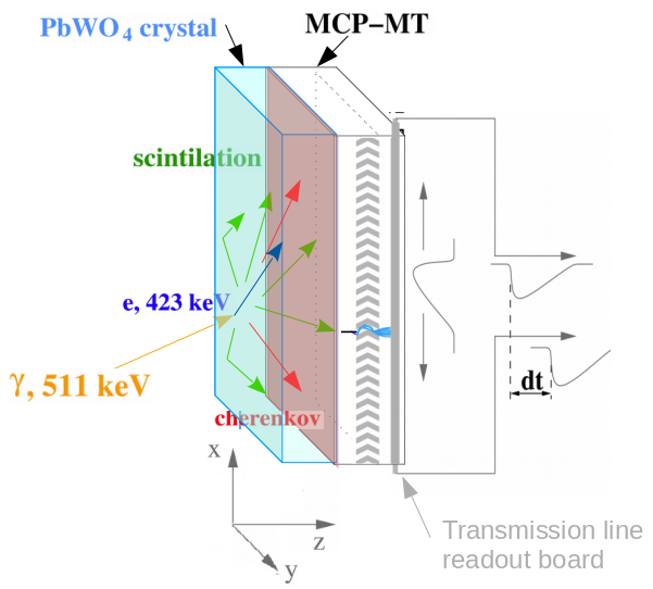
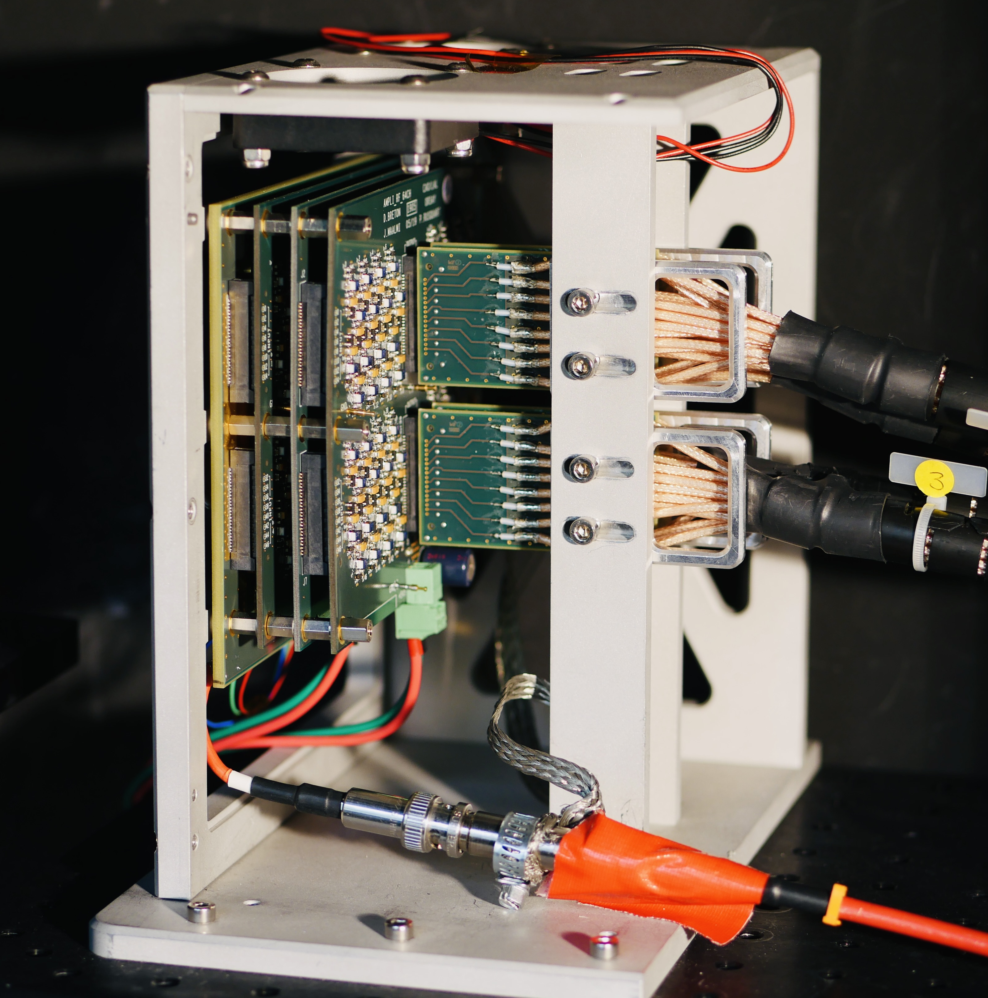
A passivation layer was deposited between the crystal and the bialkali photocathode to avoid chemical contamination of the photocathode. This PbWO4 material has a high effective atomic number of 75.6 and a density of 8.28 g/cm3. Hence it provides a short attenuation length of 9 mm for 511 keV gamma-rays and corresponds to an interaction probability of approximately 43% within a 5 mm thick crystal [12]. When an interaction occurs by Compton or photoelectric effects (Fig. 1), the gamma-ray converts into an electron that is likely to generate both, Cherenkov and scintillation photons. Among the optical photons that reach the photocathode, a fraction undergoes Fresnel reflections, while another fraction traverses the photocathode without being absorbed. Those photons that are absorbed within the photocathode have a certain probability of being converted into photoelectrons. Following the influence of the electric field, the photoelectrons undergo multiplication within the pores of the MCPs, inducing current pulses on the 4096 anode pads of the PMT. To minimize the number of electronic channels, we arranged the readout through 32 transmission lines (TLs) [13]. Each raw of 2 64 anodes pads is electrically connected to a 1.6 mm wide transmission line printed on the PCB through an anisotropic conductive rubber sheet, Inter-Connector® MT-type from Shin-Etsu [14]. The signals are read out and amplified at both ends of the transmission lines using dedicated two-stage amplifier boards (2 20 dB, 1 GHz, 50 Ohm) and recorded using a SAMPIC waveform digitizer [15, 16, 17, 18, 19].
3 Photon Detection Efficiency
In order to be able to understand the behavior of our detector, we need to define two concepts related to the photon detection efficiency of the CMP.
The first is the Normal angle Photon Detection Efficiency (NPDE), which is the ratio between the number of photoelectrons extracted from the photocathode over the number of optical photons impinging at 90° on the optical window of the photodetector as a function of the wavelength. This concept is often referred to as the quantum efficiency in many photomultiplier technical data sheets.
The second is the Intrinsic photocathode Quantum Efficiency (IQE), defined as the ratio of the number of photoelectrons extracted from the photocathode over the number of optical photons impinging at the photocathode as a function of the wavelength.
A complete photocathode model, as presented in [20, 21], requires parameterization of the optical index, absorption length, and extraction probability of photoelectrons produced within the photocathode as a function of wavelength. This is what has been implemented in the detector Monte Carlo simulation using data from [20]. Knowing the properties of the optical window, the photocathode refraction index, and when appropriate an optical passivation layer model, we are able to compute the Fresnel reflections at the optical interfaces. Then we compute the IQE of a photocathode at 90°, given an NPDE spectrum measured in [20]. Using published optical absorption lengths, and assuming a photocathode thickness of 25 nm, typical from a bi-alkali photocathode, we can compute the photoelectron extraction probability as a function of the wavelength. Variations in the NPDE, as measured in the ClearMind prototype, are implemented, by adjusting in the model a scaling factor on the photoelectron extraction probability. The above computed photocathode properties thus allow us to simulate the optical behavior of the photodetector reliably.
The ClearMind collaboration developed a test bench to measure the NPDE. The next section describes this test bench, the validation for the reference devices, and the NPDE measurement of the CMP.
3.1 Quantum efficiency measurement setup
The setup consists of a UV and VIS light source [22] that goes through a monochromator [23] for wavelength selection. The output light enters inside a dark box via 1 mm2 optical fiber and passes through a UV fused silica plano-convex lens (focal distance of 10 mm). The optical fiber output is placed at the focal point of the lens to produce a parallel light beam. An iris diaphragm is used to limit the beam size before the light reaches the detectors. The beam diameter, chosen to be 5 mm, fits within the sensitive area of the photodetector and reference photometers and was aligned to be located at the center of each photodetector. A computer-driven shutter allows the user to cut the optical beam when dark current measurements are needed.
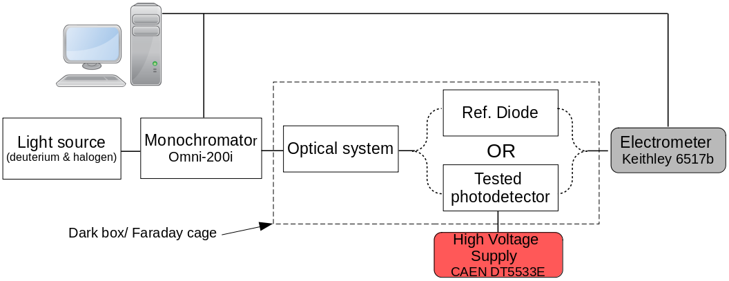
The light source is warmed up for 20 min in order to optimize its stability. During the first measurement stage, the light spot illuminates the active surface of a reference diode. In the second measurement stage, the detector under test is illuminated. The currents are read out by an electrometer Keithley 6517b [24] every second, five times per wavelength, and the average of these five measurements is stored on the PC. The layout of the experimental setup for the NPDE measurement is shown in Fig. 2.
3.1.1 Validation of the reference devices
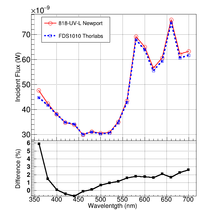
To validate the reference devices, we utilized the testbench from Fig. 2. The beam was characterized by an FS1010 Thorlabs reference diode [25] and an 818-UV/DB diode from Newport [26] used under the same conditions. As the radiant sensitivity of a reference photodetector is given by the manufacturer, we can deduct the value of the incident radiant flux from the equation:
| (3.1) |
where is the measured photocurrent. The fluxes measured by both diodes are shown in Fig. 3. Both curves are in agreement within 2 %, with the exception of wavelengths below 380 nm, where a difference up to 6 % is observed. Our measurements agree with the suppliers’ uncertainties of 5 % for Thorlabs and less than 4 % for Newport (1 % at 350). The consistency of both curves demonstrates the excellent behavior of the two diodes, the appropriate size and position of the light beam, and the light source stability.
3.2 Test cell prototype
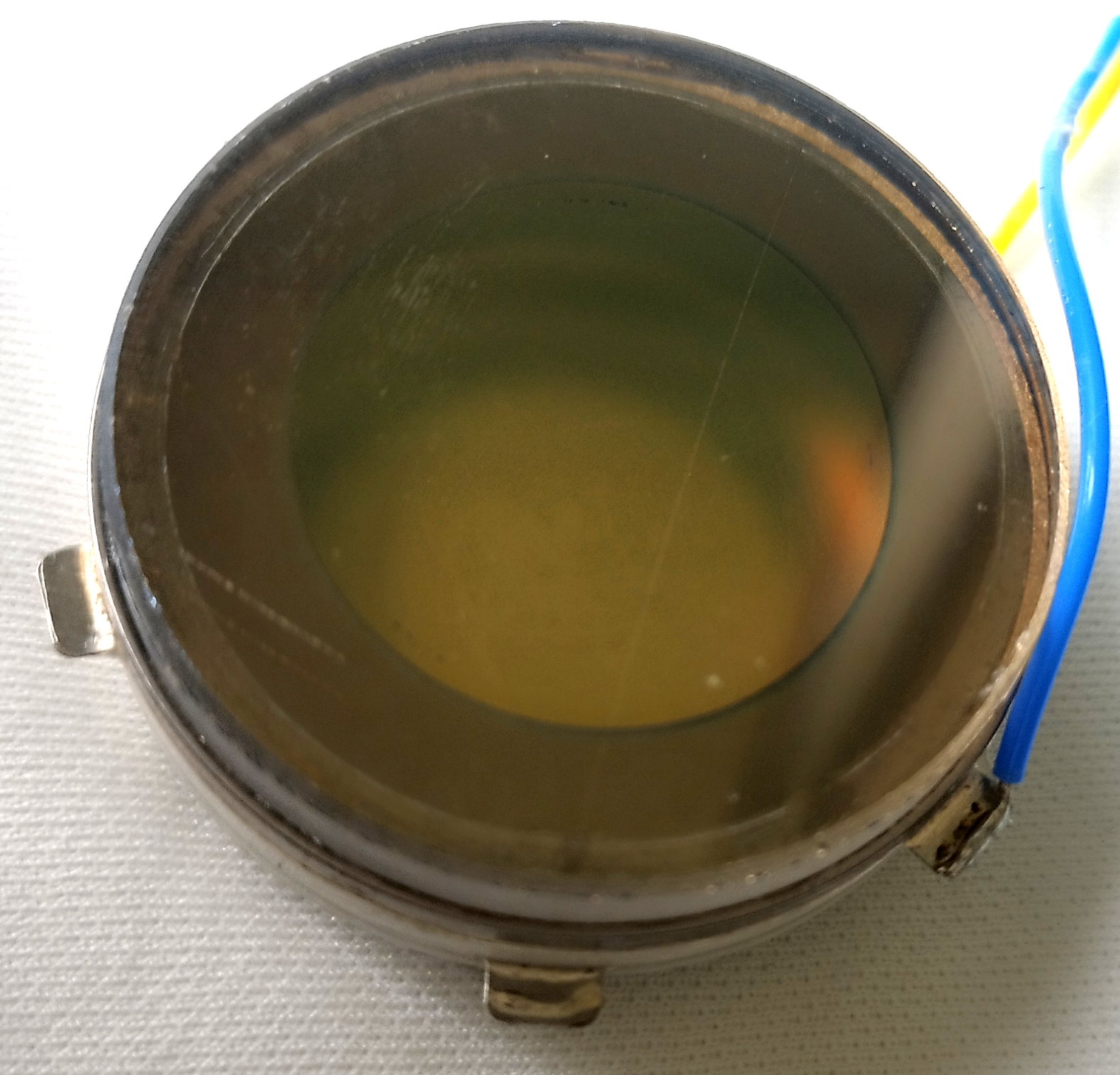
Ahead of the fabrication of the CMP, test cells were built by Photek Ltd. with a bialkali photocathode deposited on a passivated PWO optical window in order to test their performance and evaluate the feasibility of building a bigger and more complex prototype. A picture of a test cell is shown in Fig. 4 right.
We tested devices with different passivation and photocathode configurations, as this is critical for the project. These technologies are covered by a non-diffusion agreement with Photek Ltd. and thus cannot be discussed in detail in this paper. The experimental setup is the same as the one shown in Fig. 2. The NPDE of the tested photodetector, , is computed as:
| (3.2) |
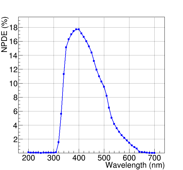
where is the quantum efficiency of the reference diode, is the current from the tested photodetector, is the reference diode current, and is the wavelength [27]. is measured directly by the test cell, and dark current is measured for each wavelength after measuring to subtract any current offset. We used the reference diode 818-UV/DB Newport to be sensitive below 350 nm. The current is directly measured at the photocathode’s output, i.e. no multiplication is carried out, and the measurement drives directly to the NPDE determination. The curve is shown in Fig. 4 left. The NPDE peaks at 18 % at a wavelength of 400 nm. The observed cut for wavelengths below 350 nm is due to the PWO being no longer transparent. The cell which was built with similar technology as the CMP, was tested for the first time in 2021 and was found to be stable over 2 years. Due to the light impinging at 90∘ with respect to the optical window, this measurement provides a convenient measurement of photocathode IQE, see Section. 3.
3.3 CMP photon detection efficiency
The measurement of implies extracting the free electron produced at the photocathode. For the CMP, a voltage of V between the photocathode and the MCP input is applied. The light beam impinges perpendicularly to the center of the CMP optical window.
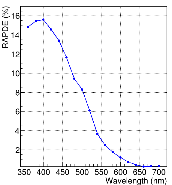
As there is no need for charge multiplication, the MCP input and output are shorted-circuited, and the current is collected directly from it. The CMP anodes matrix is grounded to a transmission line board using a Shin-Etsu MT-type of Inter-Connector® in order to avoid floating anodes and spurious currents. The output current is low-pass filtered before being measured by the electrometer. Fig. 5 shows the NPDE curve measured with the CMP, with a maximum value of 15.6 % occurring at 400 nm. The measured value will be discussed in section 6.
4 Photodetector calibration in the single photoelectron regime
4.1 Test Setup
The setup for the calibration of the CMP, performed in the single photoelectron regime, is configured as described in Section 2. The total gain from the two amplification stages is 40 dB on each one of the 64 channels. The detector and the boards are placed inside a dark/EM shielded box. A 20 ps pulsed laser PiLas by A. L. S. [28] is mounted on a 2D motion station, moved by two X-LRT0100AL-C linear stages from Zaber Technologies Inc. The laser beam, collimated with a 40 m pin-hole, impinges normally to the CMP crystal surface. The distance between the laser output and the pin-hole is 130 mm, and the distance between the pin-hole and the CMP window input is 10 mm. The light spot diameter on the optical window was calculated to be 52 m. With this configuration, the CMP operates in the single photoelectron regime with a ratio of two/one-photoelectron events of 1 %.
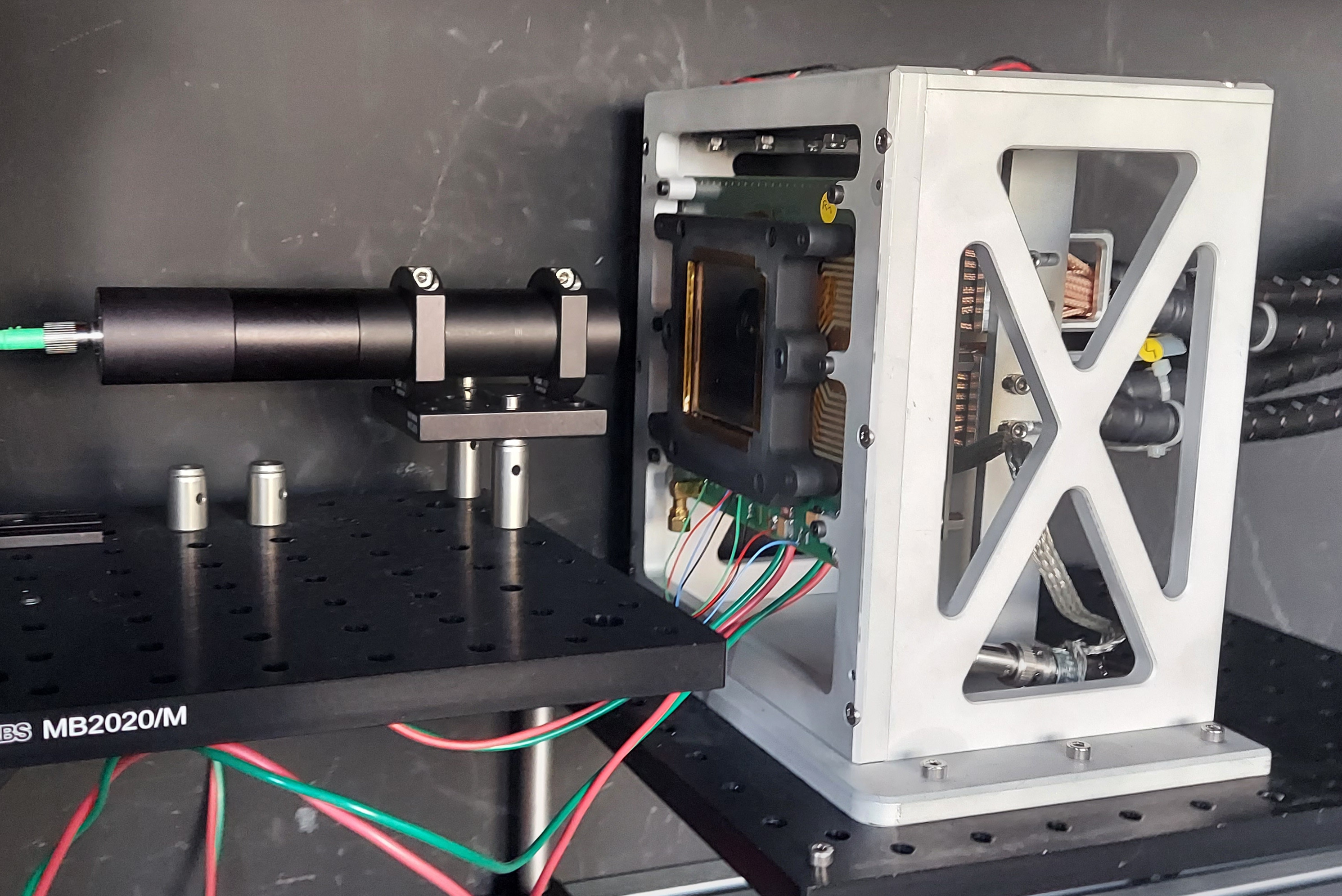
The signals were digitized by front-end boards from a SAMPIC crate @ 6.4 GS/s [17] outside of the dark box and stored on a PC. We used a 50 mV threshold level for each channel, in order to reject noise. A picture of the experimental setup is shown in Fig. 6.
We performed a laser scan using 3 mm step sizes along the -axis and 0.8 mm step sizes along the -axis, which correspond to the parallel and perpendicular coordinates with respect to the TLs orientation. For appropriate sampling, the -axis step size is chosen to be inferior to the pitch distance between the lines, which amounts to 1.66 mm. A total of 9000 different positions were scanned with an acquisition duration of 1 s for each. The events were acquired in coincidence with the output trigger of the laser.
4.2 Gain
The gain is estimated from the total charge collected at each scanned point. The charge is computed by integration of the negative part of the pulses at the end of each triggered line. The gain depends on the MCP voltage bias and is chosen to have a 2 photoelectron pulse within the sensitivity range of the SAMPIC electronics. Fig. 8 shows the number of electrons collected from the scanned CMP. The desirable pattern would be a uniform response within the surface of the PWO window. We observe a higher gain value in an upper half surface of 31 % with respect to the gain averaged. We can also observe that the area near the boundaries has 50 % less gain than the mean value. Overall, the full detection surface is responsive and active.
4.3 Time resolution
A 50 % constant fraction discrimination is used to determine the time of the pulse. The time resolution is computed as the time of the line with the highest pulse from which is subtracted the laser trigger time. From every impinging position, the time resolution histogram is fitted using the sum of 3 Gaussian functions. Fig. 9 left, shows the FWHM of the first peak (Gaussian-shaped) of these distributions. A quite homogeneous distribution is observed along the sensitive surface of the CMP, with most bins ranging from 50 to 64 ps. The larger values happen at the edges of the sensitive surface.
Fig. 9 right, shows the time resolution distribution of the CMP averaged over the whole surface. The main peak has a width of 70 ps (FWHM) and includes 63 % of the statistics. The events in the tail correspond to back-scattering electrons [29] that bounced on the first MCP surface. The time gap between the first Gaussian and the second one is directly related to the physical distance between the photocathode and the first MCP.
4.4 Event position reconstruction
The photoelectron position is calculated for the and -axes. For the coordinate perpendicular to the TLs orientation, corresponding to the -axis, we compute the weighted average of the line that has the highest pulse with its two closest neighbors, as:
| (4.1) |
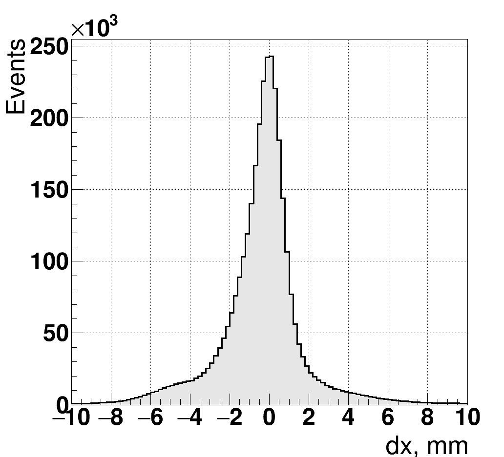
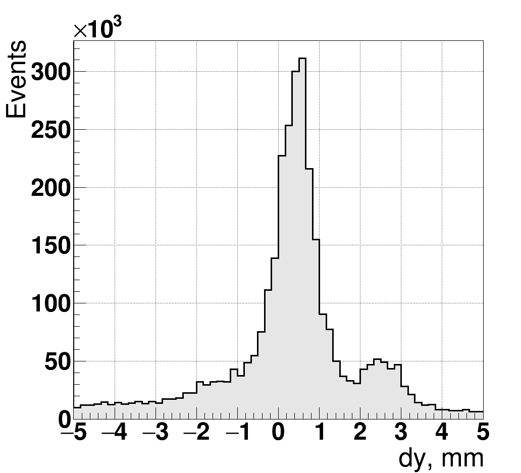
where is the -coordinate of the central TL and the charge of the -th TL. For the reconstruction on the -axis, we computed the difference between the pulse time at both ends of the line multiplied by the signal propagation speed , where and are the times of the pulses measured at the right and left ends of the -th line [13, 21]. The histograms presented in Fig. 10 show the spatial resolution along both axes over the detector’s active surface. The computed values for the resolutions on the and -axis are 1.9 mm and 1.0 mm (FWHM), respectively.
5 CMP performances under gamma-ray radiation
5.1 SiPM-LYSO reference spectrometer.
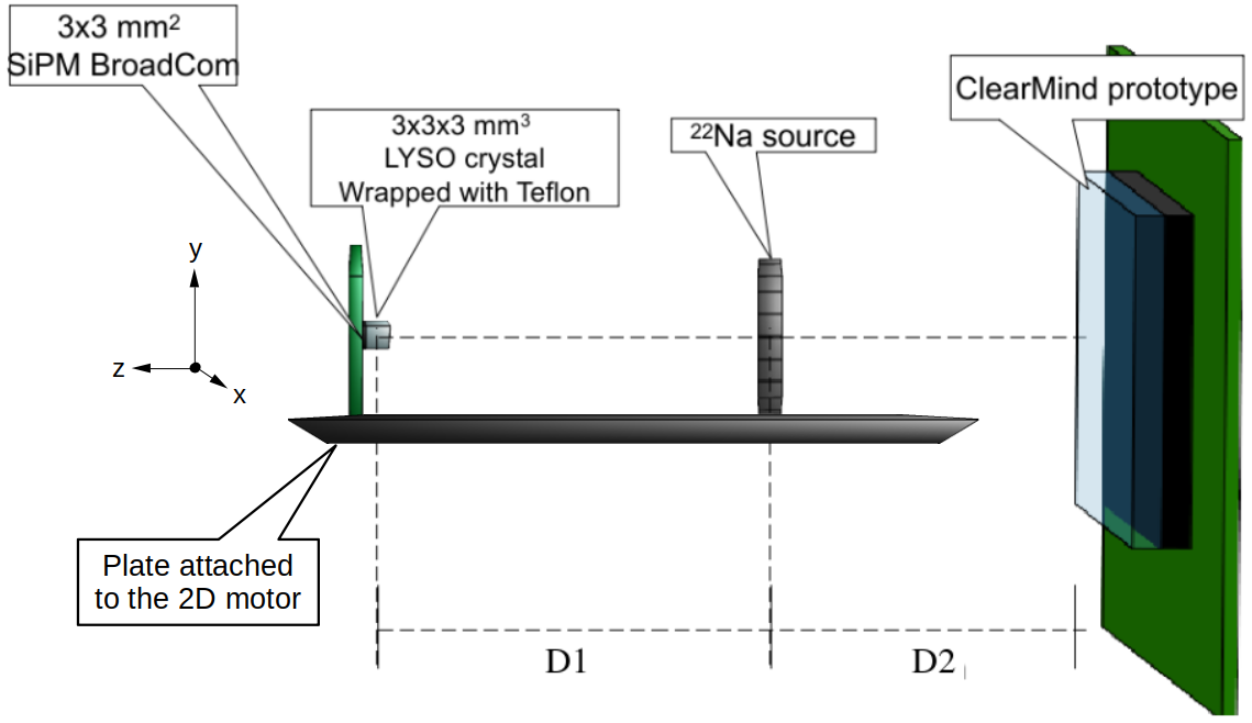
In order to select gamma-rays impinging at the surface of the CMP, a reference gamma spectrometer was needed. The spectrometer utilized for this test contains a 3 3 3 mm3 LYSO:Ca,Ce co-doped crystal from Saint-Gobain (France) [30], which features improved rise time, excellent decay time and light yield, and weaker afterglow as compared with LYSO:Ce [31]. The crystal was optically coupled with a 3 3 mm2 Broadcom SiPM using histomount glue, diluted with 2/3 of Xylène, and wrapped in Teflon tape.
A passive high-pass filter with a time constant of 2 ns was implemented at the SiPM output to remove the pulse slow time component. The time resolution measured with SAMPIC electronics is 103.5 2 ps (FWHM). The signal was then amplified using a ZKL-1R5+ amplifier [32], with a 40 dB gain, and bandwidth of 10 to 1500 MHz. After the amplification, the signal was attenuated with a passive attenuator of 3 dB model R411803124 [33], in order to match the dynamic range of the acquisition system.
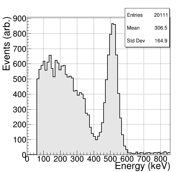
We recorded spectrometer data for a 22Na source placed 10 cm away. The SiPM was set at 18 % overvoltage. Fig. 11 shows the measured energy spectrum, where we observe a well-defined photopeak at 511 keV preceded by the Compton edge. The energy resolution measured on the photopeak is 13 % (FWHM). The signal conditioning electronics are optimized for time performance rather than amplitude and the time window for the acquisition of the pulse does not cover the entire spectrometer pulse. The energy resolution computed in this context is excellent for the purpose of our study. The conditions for the acquisition are described in more detail in the next Section.
5.2 Experimental setup
We took advantage of the test bench used for the photodetector calibration. A 22Na source was placed at a distance from the CMP. The gamma spectrometer described in Section 5.1 was placed at a distance from the source. Both, the spectrometer and the source, were mounted on a plate attached to the 2D motor station described in Section 4.1 and aligned to the CMP. The SiPM-LYSO spectrometer and the gamma-ray source were moved together across the prototype’s sensitive surface, allowing us to perform a 2D scan, as shown in Fig. 12. The boards’ stack, which includes the transmission line board and the amplification boards, is the same as described in Section 4.1. Signals coming from the CMP and the spectrometer are recorded by a SAMPIC crate at 6.4 GS/s and stored on a PC.
Energy depositions in the reference spectrometer within the range 511 keV, where keV is the FWHM of the photo-ionization peak, were considered for the analysis. The reconstruction and acquisition conditions will be described in the following Sections.
5.3 Monte Carlo simulation
In order to understand the experimental results, we developed a detailed Monte Carlo modeling of the ClearMind detector [21]. This simulation is based on the Geant4 v7.0 [34, 35, 36]. Furthermore, we developed dedicated software to model the photodetector, as well as analog and digital electronic components. The necessary parameters have been determined experimentally [9, 13]. The simulation of the detector response includes the following building blocks.
-
1.
The gamma interaction in the crystal accounts for three processes: photoelectric conversion, Compton scattering, and Rayleigh diffusion. The first two processes produce relativistic electrons that emit optical photons from the photoelectric conversion of 511 keV gamma-rays through two mechanisms: Cherenkov radiation (20 photons) and scintillation emission (165 photons).
-
2.
Every optical photon is propagated individually by the simulation. During the propagation, all the main physical effects are taken into account: photon absorption inside the PWO crystal, reflection or absorption on the crystal borders for the different types of the crystal surface (polished, absorbing), escape of photons from the crystal into the air.
-
3.
Photocathode simulation includes modeling of the crystal/photocathode transmittance [29, 37], absorption of photons by the photocathode, and extraction of generated photoelectrons as a function of the photon wavelength. As a result, we produce 12 photoelectrons on average for a 511 keV -ray photoelectric conversion in the crystal with photocathode efficiency adjusted to the values measured in Section 3.
-
4.
We then simulate the propagation and the multiplication of individual photoelectrons generated by the photocathode in the MCP-PMT and parametrize the main MCP-PMT response features: time response, MCP-PMT gain, gain fluctuation, and signal sharing between different output anodes.
-
5.
Finally, we simulate the signal readout through the transmission lines with realistic signal shapes, taking into account the possible overlay of several photoelectrons, electronics noise, and digitization sampling.
Most of the simulation parameters (single-photoelectron transition time spread, MCP-PMT gain, gain fluctuation, signal sharing between lines, etc) are adjusted to the experimental results obtained from the characterization of the CMP using a pulsed laser in the single photoelectron regime. More details about the simulation can be found elsewhere [38, 21, 39].
5.4 CMP efficiency
A high-efficiency detector is always advantageous, in particular for PET detectors [40]. For measuring the CMP’s efficiency, we set = 22 cm and = 11 cm, according to the description of Fig. 12. The source and the spectrometer remained in a single position, close to the center of the detector surface. The incoming gamma-rays could interact within the crystal either by photoelectric effect, Compton scattering, or Rayleigh diffusion. According to previous simulations, when a 511 keV gamma-ray is converted via photoelectric effect, it produces mainly a 423 keV electron and X-rays that generates 187 optical photons in total [21]. By considering that the typical MCP-PMT photoelectron collection efficiency is 90 % for these ALD-coated MCP-PMTs [41], we expect the CMP to be fully efficient at detecting photoelectron conversion. Interactions through the Compton effect generate electrons with energies below 340 keV. We have additional sensitivity for these events, particularly for the ones involving electrons with higher energies.
To estimate the detection efficiency, we used the Tag and Probe method. The 22Na radioactive source emits pairs of antiparallel 511 keV annihilation photons and most of the time a 1.27 MeV gamma-ray. The SiPM-LYSO reference spectrometer carries out the tag detection, triggers the acquisition of the SiPM spectrometers, and opens a 60 ns coincidence window allowing the acquisition of the pulses from the probe CMP. The efficiency on the probe detector is obtained as:
| (5.1) |
where is the number of events recorded by the reference spectrometer, and is the number of events recorded by the CMP.
We measured a detection efficiency = 28 3 % (only statistical errors are reported).
5.5 CMP Spatial resolution
For this measurement, the spectrometer and the radioactive source were placed at = 10 cm and = 10 cm, according to Fig. 12. The acquisition was triggered by a coincidence between the CMP and the LYSO spectrometer within a time window of 20 ns.
1
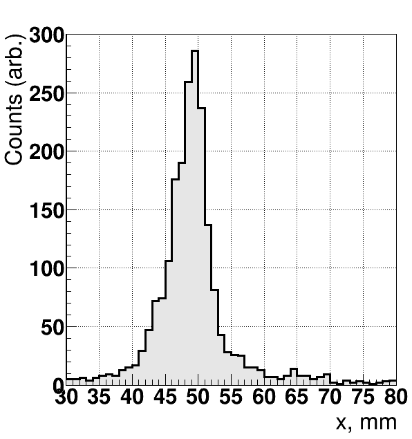
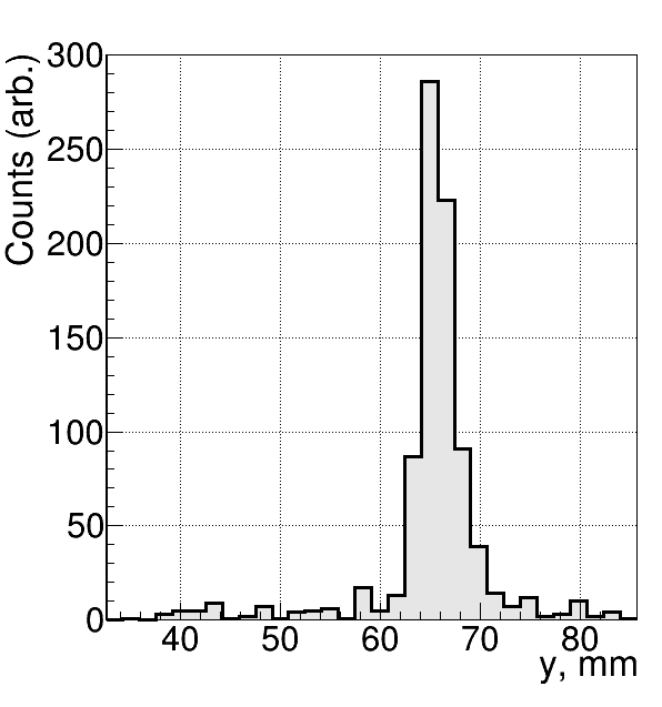
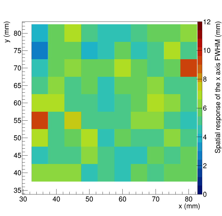
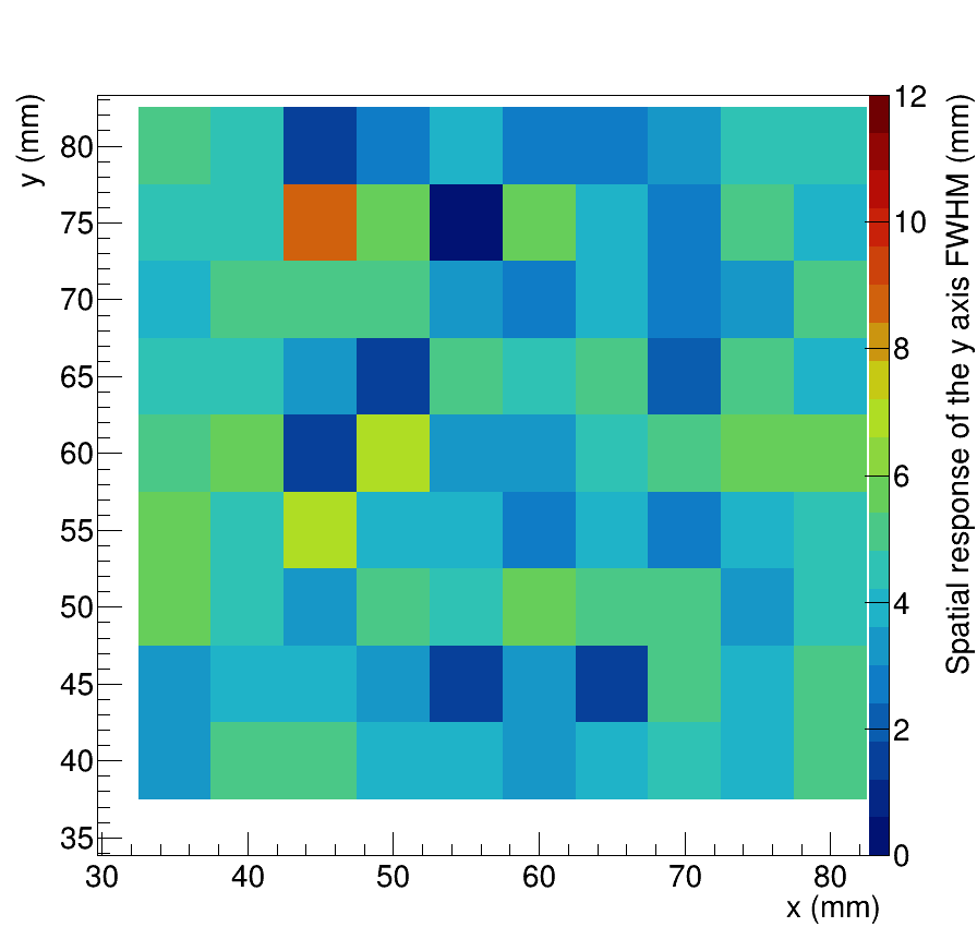
The motor stage scanned the surface of the CMP by steps of 5 cm along both axes. We acquired a 60-minute run per data point. The small solid angle of the reference spectrometer induces a trigger rate of 18 events/s. The coincidence condition with the SiPM spectrometer allows us to select 511 keV gamma-rays impinging in spot sizes of 3 mm diameter on the surface of the CMP. For the reconstruction of the interaction position, we utilized the algorithms described in Section 4.4. The typical and distributions reconstructed from a fixed position ( = 50 mm, = 65 mm), are shown in Fig. 13. The spatial resolution measured for the -axis parallel to the TLs is 5.4 mm (FWHM) and the spatial resolution measured for the -axis perpendicular to the TLs is 3.5 mm (FWHM). Fig. 14 shows the spatial resolution as a function of the source position. We observe a uniform distribution of the spatial resolution along the -axis, with a computed mean of 5.2 mm FWHM on the surface. We computed a mean of 4 mm FWHM for the spatial resolution for the -axis, with a reasonable uniformity.
5.6 CMP time response
To measure the detector time resolution, we used the same data collection from the setup described in Section 5.5.
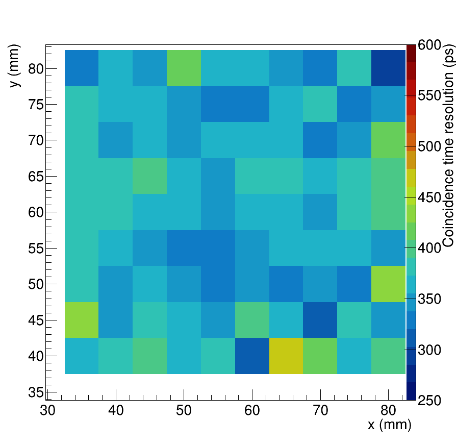
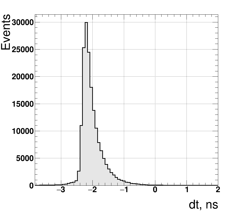
We selected events with 12 or more triggered lines, primarily arising from photoionization events. The distribution of the time difference between the spectrometer signal and the fastest pulse recorded in coincidence for the CMP is shown in Fig. 15. We observe a consistent CTR response for the majority of source positions, with typical values around 350 ps, corresponding to the prototype resolution of 330 ps. The distribution of the average over all the source positions is shown in Fig. 15 on the right with a CTR of 370 ps.
6 Discusion
This study presents the first successful attempt to improve photon extraction probability from a PWO crystal through the direct deposition of a bialkali photocathode onto its surface. The feasibility of bialkali deposition on PWO proved to be challenging. After optimization of the passivation layer [8, 9] between the crystal and the photocathode, an NPDE of 18 % at 400 nm was demonstrated. The test cell presented in Section 3.2 was produced in 2021, and showed no significant efficiency variations over time. Moreover, this value is close to the value measured in the CMP and the value reported on [37].
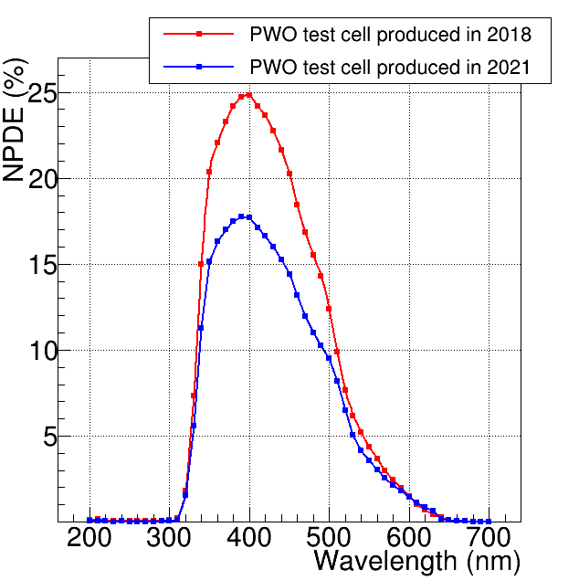
The CMP, which is described in Section 2, serves as a compelling demonstration of the feasibility of this technique for constructing a scanner-sized detection module. Regrettably, this prototype exhibits limited optical photon detection efficiency, as presented in Section 3.3. As mentioned earlier, the test cell exhibits long-term photocathode stability. Moreover, a test cell produced in 2018 with a similar photocathode configuration, performs an NPDE of 25 % at 400 nm, as shown in Fig. 16. This test cell presented stability over 4 years. Unfortunately, Photek Ltd. has not been able to reproduce a CMP with this NPDE until now. Nevertheless, future hardware efforts will focus on achieving 25 % NPDE or more for future prototypes and improving the passivation layer, hence improving the optical light collection efficiency and the global detector performances.
We estimated the photoelectric interaction probability of a gamma-ray within the 5 mm PWO crystal of about 21.5 %. Simulations showed that, from the expected 187 optical photons generated for a photoelectric interaction of a 511 keV gamma-ray, approximately 85 photons are absorbed by the photocathode and around 13 photons are converted into photoelectrons [21]. With this amount of photoelectrons and the high MCP-PMT collection efficiency, we are fully efficient for detecting gamma-rays interacting via the photoelectric effect. The high Compton interaction probability of 25.2 % for 511 keV gamma-rays passing through the 5 mm PWO crystal contributes to the total detection efficiency, which was measured to be %. This estimation is consistent with the estimation from simulations, of 28.6 %. By increasing the PWO crystal thickness to 10 mm, the photoelectric interaction probability would increase to 38.8 %, while the Compton interaction probability would rise to 44 %, leading to an overall efficiency improvement, surpassing 40 %.
The reconstruction of the source position presented in this paper was computed using basic algorithms that demonstrate the possibility of reconstructing the source position with the proposed readout scheme. The collaboration is continuously working on optimizing the reconstruction of the interaction position including depth of interaction using neural networks. These methods demonstrated a great potential for improving the reconstruction of the interaction positions on Monte Carlo simulated events [42]. The improved version of the ClearMind detection module will incorporate an additional photosensor layer, such as a SiPM array, on the open front side of the crystal. This addition will enable us to enhance detection efficiency and, more importantly, to achieve high-precision reconstruction of the depth of interaction, as described in [8].
With the ClearMind detection paradigm, achieving precise timing is the ultimate goal, which could be reached through the detection of Cherenkov photons. Time resolution is thus driven mainly by the MCP-PMT single photoelectron transit time spread and the number of Cherenkov photons detected. Monte Carlo simulations demonstrated that 45 % of the Cherenkov photons generated from photoelectron conversion reach the photocathode [21]. From the NPDE measured in CMP, we expect to detect about 0.7 Cherenkov photons on average when applying a selection on the number of lines. This value corresponds to a probability of 48 % of containing at least one Cherenkov photoelectron. This modest value limits the time resolution achieved with CMP to 330 ps FWHM. As mentioned above, we are actively working on improving the photocathode efficiency. Additionally, we plan to equip the free side of the crystal with a thin detection layer. Those upgrades will boost the number of photons detected and improve the overall performance of our system.
7 Conclusions
In this study, we investigate the possibility of improving the timing performance of the PET detection module using Cherenkov photons while optimizing the optical interface by direct deposition of the photocathode on the PWO crystal. We proved the feasibility of direct photocathode deposition on a PWO crystal, with an efficiency of 18 %, and demonstrated its stability over time.
We succeeded in creating a fully functional detection module. This prototype has an excellent single photoelectron time resolution of 70 ps FWHM all over its surface, spatial resolutions of 1.9 mm FWHM for the x-axis parallel to the TLs, and 1.0 mm FWHM in the perpendicular direction. We tested the ClearMind prototype performance for detecting 511 keV gamma-rays and demonstrated the capability to reconstruct the source position, with a spatial resolution of 4 to 5 mm FWHM, using a simple reconstruction algorithm. This work is carried on by developing artificial intelligence reconstruction in order to achieve better resolutions, as well as for the estimation of the gamma-ray depth of interaction. CMP has non-optimal photocathode quantum efficiency, which limits the time resolution to 330 ps. The ClearMind technology will be upgraded in the future, as described in Section 6, in order to improve the performance of the detection module.
Acknowledgments
The authors would like to thank Saint-Gobain Crystals for kindly providing the LYSO:Ce:Ca single crystals used to build reference spectrometers [30]. We are grateful for the support and seed funding from the CEA, Programme Exploratoire Bottom-Up, under grant No. 17P103- CLEAR-MIND, and the French National Research Agency under the grant No. ANR-19-CE19-0009-01. Chi-Hsun Sung, Ph.D. is supported by the CEA NUMERICS program, which has received funding from the European Union’s Horizon 2020 research and innovation program under the Marie Sklodowska-Curie grant agreement No. 800945 - (NUMERICS - H2020-MSCA-COFUND- 2017).
References
- Jiang et al. [2019] Wei Jiang, Yamn Chalich, and M. Jamal Deen. Sensors for positron emission tomography applications. Sensors (Basel, Switzerland), 19, November 2019. URL https://doi.org/10.3390%2Fs19225019.
- Ullah et al. [2016] Muhammad Nasir Ullah, Eva Pratiwi, Jimin Cheon, Hojong Choi, and J. Y. Yeom. Instrumentation for time-of-flight positron emission tomography. Nuclear Medicine and Molecular Imaging, 50:112–122, 2016. URL https://doi.org/10.1007%2Fs13139-016-0401-5.
- Snyder et al. [1981] Donald L. Snyder, Lewis J. Thomas, and Michel M. Ter-Pogossian. A matheematical model for positron-emission tomography systems having time-of-flight measurements. IEEE Transactions on Nuclear Science, 28(3):3575–3583, 1981. doi: 10.1109/TNS.1981.4332168.
- Budinger [1983] Thomas Budinger. Time-of-flight positron emission tomography: status relative to conventional pet. Journal of nuclear medicine : official publication, Society of Nuclear Medicine, 24 1:73–8, 1983. URL https://api.semanticscholar.org/CorpusID:671110.
- Lecoq [2017] P. Lecoq. Pushing the limits in time-of-flight pet imaging. IEEE Transactions on Radiation and Plasma Medical Sciences, 1(6):473–485, 2017. URL https://doi.org/10.1109/TRPMS.2017.2756674.
- Lecoq et al. [2020] Paul Lecoq, Christian Morel, John O. Prior, Dimitris Visvikis, Stefan Gundacker, Etiennette Auffray, Peter Križan, Rosana Martinez Turtos, Dominique Thers, Edoardo Charbon, Joao Varela, Christophe De La Taille, Angelo Rivetti, Dominique Breton, Jean François Pratte, Johan Nuyts, Suleman Surti, Stefaan Vandenberghe, Paul Marsden, Katia Parodi, Jose Maria Benlloch, and Mathieu Benoit. Roadmap toward the 10 ps time-of-flight pet challenge. Physics in Medicine and Biology, 65(21), November 2020. ISSN 0031-9155. doi: 10.1088/1361-6560/ab9500.
- van Sluis et al. [2019] Joyce van Sluis, J. de Jong, Jenny Schaar, Walter Noordzij, Paul J.H. van Snick, Rudi A. Dierckx, Ronald J. H. Borra, Antoon T. M. Willemsen, and Ronald Boellaard. Performance characteristics of the digital biograph vision pet/ct system. The Journal of Nuclear Medicine, 60:1031 – 1036, 2019. URL https://doi.org/10.2967/jnumed.118.215418.
- Yvon et al. [2020] D. Yvon, V. Sharyy, M. Follin, J.P. Bard, D. Breton, J. Maalmi, C. Morel, and E. Delagnes. Design study of a “scintronic” crystal targeting tens of picoseconds time resolution for gamma ray imaging: the ClearMind detector. JINST, 15(07):P07029, 2020. URL https://hal.science/hal-02899246.
- Follin et al. [2021] M. Follin, V. Sharyy, J-P. Bard, M. Korzhik, and D. Yvon. Scintillating properties of today available lead tungstate crystals. JINST, 16(08):P08040, 2021. doi: 10.1088/1748-0221/16/08/P08040. URL https://hal.science/hal-03197498.
- CRYTUR [2023] CRYTUR. spol. s r.o. Na Lukách 2283 51101 Turnov Czech Republic, 2023. URL https://www.crytur.com.
- Ltd. [2023] Photek Ltd. MAPMT-253 Multi-Anode MCP-PMT Datasheet, 2023. URL https://www.photek.com/pdf/datasheets/detectors/Auratek-Square-Detector-13SEP17.pdf.
- Berger et al. [2010] Martin Berger, J Hubbell, Stephen Seltzer, J Coursey, and D Zucker. Xcom: Photon cross section database, 2010. URL http://physics.nist.gov/xcom.
- Follin et al. [2022] M. Follin, R. Chyzh, C.-H. Sung, D. Breton, J. Maalmi, T. Chaminade, E. Delagnes, K. Schäfers, C. Weinheimer, D. Yvon, and V. Sharyy. High resolution MCP-PMT readout using transmission lines. Nuclear Instruments and Methods in Physics Research Section A: Accelerators, Spectrometers, Detectors and Associated Equipment, 1027:166092, mar 2022. URL https://doi.org/10.1016/j.nima.2021.166092.
- SHIN-ETSU [2023] SHIN-ETSU. MT-Type of Inter-Connector Datasheet, 2023. URL https://www.shinetsu.info/product/mt-type-of-inter-connector/?attachment_id=1687&download_file=d2bw67wo7s226.
- Breton [March 2014] Dominique Breton. Measuring time with a 5-ps precision at the systel level with the WaveCatcher family of SCA-based fast digitizers. In Workshop in picosecond photon sensors for physics and medical application, March 2014. URL https://indico.cern.ch/event/306859/session/3/contribution/9/material/slides/1.pdf.
- Delagnes et al. [March 2014] E. Delagnes, H. Grabas, D. Breton, and J. Maalmi. The sampic WTDC chip. Workshop on Picosecond Photon Sensors for physics and medical application, March 2014.
- Delagnes et al. [2015] E. Delagnes, D. Breton, H. Grabas, J. Maalmi, and P. Rusquart. Reaching a few picosecond timing precision with the 16-channel digitizer and timestamper SAMPIC ASIC. Nucl. Instrum. Meth. A, A787:245–249, 2015. doi: 10.1016/j.nima.2014.12.042.
- Breton et al. [2016] D. Breton, V. De Cacqueray, E. Delagnes, H. Grabas, J. Maalmi, N. Minafra, C. Royon, and M. Saimpert. Measurements of timing resolution of ultra-fast silicon detectors with the SAMPIC waveform digitizer. Nucl. Instrum. Meth. A, 835(Supplement C):51–60, 2016. ISSN 0168-9002. doi: 10.1016/j.nima.2016.08.019.
- Breton et al. [2020] D. Breton, C. Cheikali, E. Delagnes, J. Maalmi, P. Rusquart, and P. Vallerand. Fast electronics for particle Time-Of-Flight measurement, with focus on the SAMPIC ASIC. Nuovo Cimento C, 43(1):7, 2020. doi: 10.1393/ncc/i2020-20007-6.
- Motta and Schonert [2005] Dario Motta and Stefan Schonert. Optical properties of Bialkali photocathodes. Nucl. Instrum. Meth. A, A539:217–235, 2005. doi: 10.1016/j.nima.2004.10.009.
- Sung et al. [2023] C.-H. Sung, L. Cappellugola, M. Follin, S. Curtoni, M. Dupont, C. Morel, A. Galindo-Tellez, R. Chyzh, D. Breton, J. Maalmi, D. Yvon, and V. Sharyy. Detailed simulation for the clearmind prototype detection module and event reconstruction using artificial intelligence. Nuclear Instruments and Methods in Physics Research Section A: Accelerators, Spectrometers, Detectors and Associated Equipment, 1053:168357, August 2023. ISSN 0168-9002. doi: https://doi.org/10.1016/j.nima.2023.168357. URL https://www.sciencedirect.com/science/article/pii/S0168900223003479.
- Ocean Optics [2023] Inc. Ocean Optics. DH-2000-BAL Light Source, 2023. URL https://www.oceaninsight.com/products/light-sources/uv-vis-nir-light-sources/dh-2000-bal/?qty=1.
- Zolix Instruments Co. [2023] Ltd. Zolix Instruments Co. Omni-200i, 2023. URL https://www.zolix.com.cn/en/prodcon_370_376_741.html.
- Instruments [2023] Keithley Instruments. Electrometer Model 6517B, 2023. URL https://www.tek.com/en/datasheet/6517b-electrometer-high-resistance-meter.
- Thorlabs [2023] Inc. Thorlabs. FDS1010 Si detector Datasheet, 2023. URL https://www.thorlabs.com/drawings/51e19728c72ae1ee-36153490-E029-7FE0-DB9940D12A2CABE3/FDS1010-CAL-SpecSheet.pdf.
- Corporation. [2022] Newport Corporation. 818-UV/DB detector Datasheet, 2022. URL https://www.newport.com/medias/sys_master/images/images/hbd/h46/9599504875550/DS-051502-818-Series-Photodiode-Datasheet.pdf.
- K.K. [2017] Hamamatsu Photonics K.K. PHOTOMULTIPLIER TUBES, Basics and Applications. Hamamatsu Photonics K.K. Electron Tube Division, 2017. URL https://www.hamamatsu.com/content/dam/hamamatsu-photonics/sites/documents/99_SALES_LIBRARY/etd/PMT_handbook_v4E.pdf.
- GmbH [2017] Advansed Laser Diode System A.L.S. GmbH. Picosecond diode laser - pilas, manual and test report cea PiL040XSM-1_825, 2017. URL https://www.nktphotonics.com/products/pulsed-diode-lasers/pilas/.
- Chen et al. [2018] Ping Chen, Jinshou Tian, Lehui Guo, Yonglin Wei, Hulin Liu, Xiaofeng Sai, Xing Wang, Yu Lu, Chao Wang, Junfeng Wang, Kai He, Liping Tian, Liwei Xin, and Haitao Guo. Photoelectron backscattering in the microchannel plate photomultiplier tube. Nuclear Instruments and Methods in Physics Research Section A: Accelerators, Spectrometers, Detectors and Associated Equipment, 912:112–114, December 2018. doi: 10.1016/j.nima.2017.10.081. URL https://www.sciencedirect.com/science/article/pii/S0168900217311701.
- sai [2023] Saint-Gobain, France, 2023. URL https://www.crystals.saint-gobain.com.
- Blahuta et al. [2013] S. Blahuta, A. Bessière, B. Viana, P. Dorenbos, and V. Ouspenski. Evidence and consequences of Ce 4+ in LYSO:Ce,Ca and LYSO:Ce,Mg single crystals for medical imaging applications. IEEE Transactions on Nuclear Science, 60(4):3134–3141, 2013. doi: 10.1109/TNS.2013.2269700. URL https://doi.org/10.1109/TNS.2013.2269700.
- Mini-Circuits. [2023] Mini-Circuits. Coaxial amplifier zkl-1r5+, datasheet, 2023. URL https://www.minicircuits.com/pdfs/ZKL-1R5.pdf.
- Radiall. [2023] Radiall. 3db attenuator, datasheet, 2023. URL https://www.farnell.com/datasheets/2092151.pdf.
- Agostinelli et al. [2003] S. Agostinelli et al. GEANT4: A Simulation toolkit. Nucl. Instrum. Meth. A, 506:250–303, 2003. doi: 10.1016/S0168-9002(03)01368-8. URL https://www.sciencedirect.com/science/article/abs/pii/S0168900203013688?via%3Dihub.
- Allison et al. [2006] J. Allison, K. Amako, J. Apostolakis, H. Araujo, P. Arce Dubois, M. Asai, G. Barrand, R. Capra, S. Chauvie, R. Chytracek, G. A. P. Cirrone, G. Cooperman, G. Cosmo, G. Cuttone, G. G. Daquino, M. Donszelmann, M. Dressel, G. Folger, F. Foppiano, J. Generowicz, V. Grichine, S. Guatelli, P. Gumplinger, A. Heikkinen, I. Hrivnacova, A. Howard, S. Incerti, V. Ivanchenko, T. Johnson, F. Jones, T. Koi, R. Kokoulin, M. Kossov, H. Kurashige, V. Lara, S. Larsson, F. Lei, O. Link, F. Longo, M. Maire, A. Mantero, B. Mascialino, I. McLaren, P. Mendez Lorenzo, K. Minamimoto, K. Murakami, P. Nieminen, L. Pandola, S. Parlati, L. Peralta, J. Perl, A. Pfeiffer, M. G. Pia, A. Ribon, P. Rodrigues, G. Russo, S. Sadilov, G. Santin, T. Sasaki, D. Smith, N. Starkov, S. Tanaka, E. Tcherniaev, B. Tome, A. Trindade, P. Truscott, L. Urban, M. Verderi, A. Walkden, J. P. Wellisch, D. C. Williams, D. Wright, and H. Yoshida. Geant4 developments and applications. IEEE Trans. Nucl. Sci., 53(1):270–278, February 2006. ISSN 1558-1578. doi: 10.1109/TNS.2006.869826. URL https://ieeexplore.ieee.org/document/1610988.
- Allison et al. [2016] J. Allison, K. Amako, J. Apostolakis, P. Arce, M. Asai, T. Aso, E. Bagli, A. Bagulya, S. Banerjee, G. Barrand, B. R. Beck, A. G. Bogdanov, D. Brandt, J. M. C. Brown, H. Burkhardt, Ph. Canal, D. Cano-Ott, S. Chauvie, K. Cho, G. A. P. Cirrone, G. Cooperman, M. A. Cortés-Giraldo, G. Cosmo, G. Cuttone, G. Depaola, L. Desorgher, X. Dong, A. Dotti, V. D. Elvira, G. Folger, Z. Francis, A. Galoyan, L. Garnier, M. Gayer, K. L. Genser, V. M. Grichine, S. Guatelli, P. Guèye, P. Gumplinger, A. S. Howard, I. Hřivnáčová, S. Hwang, S. Incerti, A. Ivanchenko, V. N. Ivanchenko, F. W. Jones, S. Y. Jun, P. Kaitaniemi, N. Karakatsanis, M. Karamitros, M. Kelsey, A. Kimura, T. Koi, H. Kurashige, A. Lechner, S. B. Lee, F. Longo, M. Maire, D. Mancusi, A. Mantero, E. Mendoza, B. Morgan, K. Murakami, T. Nikitina, L. Pandola, P. Paprocki, J. Perl, I. Petrović, M. G. Pia, W. Pokorski, J. M. Quesada, M. Raine, M. A. Reis, A. Ribon, A. Ristić Fira, F. Romano, G. Russo, G. Santin, T. Sasaki, D. Sawkey, J. I. Shin, I. I. Strakovsky, A. Taborda, S. Tanaka, B. Tomé, T. Toshito, H. N. Tran, P. R. Truscott, L. Urban, V. Uzhinsky, J. M. Verbeke, M. Verderi, B. L. Wendt, H. Wenzel, D. H. Wright, D. M. Wright, T. Yamashita, J. Yarba, and H. Yoshida. Recent developments in Geant4. Nucl. Instrum. Meth. A, 835:186–225, 2016. ISSN 0168-9002. doi: 10.1016/j.nima.2016.06.125. URL https://www.sciencedirect.com/science/article/pii/S0168900216306957.
- Cappellugola [2023] Laurie Cappellugola. Modélisation monte carlo d’un détecteur scintronique à haute résolution spatio-temporelle couplé à un tube multiplicateur à galette de micro-canaux, phd thesis, 2023. URL https://theses.fr/s301206.
- Sung [2022] Chi-Hsun Sung. Simulation and artificial intelligence for a gamma detector for high resolution PET imaging. PhD thesis, Université Paris-Saclay, 2022. URL http://www.theses.fr/2022UPASP060.
- Cappellugola et al. [2021] L. Cappellugola, S. Curtoni, M. Dupont, C.-H. Sung, V. Sharyy, C. Thibault, D. Yvon, and C. Morel. Modelisation of Light Transmission through Surfaces with Thin Film Optical Coating in Geant4. In 2021 IEEE Nuclear Science Symposium and Medical Imaging Conference (NSS/MIC), pages 1–5. IEEE, 2021. doi: 10.1109/NSS/MIC44867.2021.9875513. URL https://ieeexplore.ieee.org/document/9875513.
- Canot et al. [2019] C. Canot, M. Alokhina, P. Abbon, J.P. Bard, D. Breton, E. Delagnes, J. Maalmi, G. Tauzin, D. Yvon, and V. Sharyy. Fast and efficient detection of 511 keV photons using Cherenkov light in PbF2 crystal, coupled to a MCP-PMT and SAMPIC digitization module. Journal of Instrumentation, 14(12):P12001, dec 2019. doi: 10.1088/1748-0221/14/12/P12001. URL https://dx.doi.org/10.1088/1748-0221/14/12/P12001.
- Lehmann et al. [2022] A. Lehmann, M. Böhm, D. Miehling, M. Pfaffinger, S. Stelter, F. Uhlig, A. Ali, A. Belias, R. Dzhygadlo, A. Gerhardt, M. Krebs, D. Lehmann, K. Peters, G. Schepers, C. Schwarz, J. Schwiening, M. Traxler, M. Düren L. Schmitt d, E. Etzelmüller, K. Föhl, A. Hayrapetyan, K. Kreutzfeld, J. Rieke, M. Schmidt, T. Wasem, and C. Sfienti. Latest technological advances with MCP-PMTs. Journal of Physics: Conference Series, 2374:012128, 2022. doi: 10.1088/1742-6596/2374/1/012128. URL https://iopscience.iop.org/article/10.1088/1742-6596/2374/1/012128/pdf.
- Daniel et al. [2003] Geoffrey Daniel, Mohamed Bahi Yahiaoui, Claude Comtat, Sebastien Jan, Olga Kochebina, Jean-Marc Martinez, Viktoriya Sergeyeva, Viatcheslav Sharyy, Chi-Hsun Sung, and Dominique Yvon. Deep learning reconstruction with uncertainty estimation for photon interaction in fast scintillator detectors. Submitted to Engineering Applications of Artificial Intelligence., 2003. doi: 10.48550/arXiv.2310.06572. URL https://arxiv.org/abs/2310.06572.