Photovoltaic efficiency of transition metal dichalcogenides thin films by ab initio excited-state methods
Abstract
Transition metal dichalcogenides (TMDCs) have garnered significant interest in optoelectronics, owing to their scalability and thickness-dependent electrical and optical properties. In particular, thin films of TMDCs could be used in photovoltaic devices. In this work, we employ ab initio many-body perturbation theory within -BSE approach to accurately compute the optoelectronic properties of thin films of 2H-TMDCs composed of Mo, W, S, and Se. Subsequently, we evaluate their photovoltaic performance including exciton recombination effects, and show this is a key ingredient. We obtain efficiencies of up to 29% for a 200-nm thick film of \ceWSe2, thus providing an upper limit. We also include other phenomenological recombination mechanisms that could be present in current samples. This slightly reduces efficiencies, indicating that even with current synthesis technologies, there is still potential for further enhancement of TMDCs’ performance in photovoltaic applications.
keywords:
Suggested keywordsKeywords: Transition metal dichalcogenides Photovoltaic efficiency Optoelectronics Thin films MBPT -BSE
1 Introduction
Layered van der Waals (vdW) materials consist of stacked two-dimensional (2D) sheets interacting via dispersion forces. Graphite is a well-known member of this family that is broadly used in industry as components for electrodes, lubricants, fibers, heat exchangers, and batteries 1. The experimental isolation of its single-layer counterpart, graphene 2 has opened the way for a new era of 2D materials with compelling optoelectronic properties 3, 4, 5. However, the lack of an energy gap in graphene greatly limits its applicability in semiconductor technologies. On the other hand, the semiconducting properties of transition metal dichalcogenides (TMDCs), with chemical formula \ceMX2 (M = Mo, W, and others, and X = S, Se, Te) pushed the frontier of vdW materials’ potential uses spanning a broad range of fields, including nanoelectronics and nanophotonics, sensing and actuation in the nanoscale, and photovoltaic solar cells 6, 7, 8, 9, 10, 11, 12.
The TMDCs monolayers present direct bandgaps ranging from to eV 13, which is well-suited for solar energy absorption 14, particularly as ultra-thin photon absorbers for applications in transparent and flexible solar cells 15, 16. Theoretical predictions indicate that the TMDCs monolayers should present absorption coefficients per unit thickness one to two orders of magnitude greater than those of conventional semiconductors 17. This is achieved due to the localized nature of electronic wave functions, leading to van Hove singularities in the density of states. These strong peaks are accountable for the heightened photoresponsivity observed in these 2D materials 18. As a consequence, with a thickness of less than 1 nm, in principle, they can absorb an amount of visible light comparable to 15 nm of GaAs or 50 nm of Si 17, which makes them a promising choice for efficient photovoltaic applications. However, in practice, the power conversion efficiency (PCE) of single layer TMDC solar cells has typically not exceeded 2% 19, 20, 21, 22, 23, 24. This is mostly due to strong Fermi-level pinning at the metal–semiconductor interface 25, and high probability of carrier recombination caused by defective surfaces, which leads to a low open-circuit voltage () 15.
In order to overcome those performance issues, some TMDC-based solar cells have been assembled by using few-layered or multi-layered stacks of 2H-TMDCs. Lee et al. 26 have studied the photovoltaic response of graphene-sandwiched \ceMoS2/\ceWSe2 heterostructures with different thicknesses. They reported a high short-circuit current density of A/cm2, measured under laser light ( nm). For comparison, the authors also reported the short-circuit current of vertical heterojunctions composed of single atomic layers of \ceMoS2 (-doped) and \ceWSe2 (either -doped or ambipolar) with a value of mA/cm2. The external quantum efficiency (EQE) is also dependent on the number of layers. The measured EQEs at 532 nm were 2.4%, 12%, and 34% for monolayer, bilayer, and multilayer p–n junctions. Memaran et al. 27 have studied the photovoltaic efficiency of the \ceMoSe2 crystal composed of atomic layers transferred onto a flat hBN crystal creating an electrostatic p-n junction. They have reported photovoltaic efficiencies surpassing 14% under AM-1.5 spectrum, with concomitant fill factors approaching 0.7.
More recently, Cho et al. 28 proposed a transparent thin-film photovoltaic cell composed by a heterojunction of \ceWSe2/\ceMoS2 and an indium tin oxide electrode. Their device is highly transparent () and presents a PCE of 10%. Also, high-specific-power flexible transition metal dichalcogenide solar cells have been fabricated by employing transparent graphene contacts and \ceMoO_x capping for doping, passivation, and anti-reflection 29. These lead to PCE of 5.1% and specific power of 4.4 Wg-1 for flexible \ceWSe2 solar cells.
These observations suggest that junctions composed of few-layered or multilayered TMDCs can yield higher photovoltaic responses compared to monolayers. Nonetheless, while monolayer TMDCs have been extensively studied and well characterized for photovoltaic applications, their bulk counterparts were less so, especially from a microscopic point of view. In this sense, a highly accurate and reliable ab initio prediction of the optoelectronic properties and photovoltaic efficiencies of bulk 2H-TMDCs is crucial.
Herein, we employ ab initio many-body perturbation theory within the -BSE scheme to investigate the optoelectronic properties of bulk 2H-TMDCs and then address their theoretical photovoltaic efficiencies. We analyze the power-conversion efficiency of \ceMX_2 TMDCs with M = Mo, W and X = S, Se, modeling the inclusion of nonradiative recombination losses with exciton eigenvalues computed by BSE, in an approach we denote as SLME-X which has already been proposed by Ozório and co-workers 30, and compared those results with another modeling in which we estimate the fraction of radiative recombination processes using reported values obtained by photoluminescence quantum yield experiments (SLME-PLQY). Applying the SLME-X approach, the photovoltaic efficiencies of the TMDCs consistently fell within the range of 23% to 29%, reaching efficiencies analogous to those obtained using the Shockley-Queisser formalism. On the other hand, when we employ the SLME-PLQY framework, the power conversion efficiencies tend to be reduced, ranging from 19% to 24%.
2 Computational Methods
Ground-state atomic structures were obtained by first-principles calculations based on density-functional theory (DFT) 31, 32 as implemented in the quantum espresso package 33. The Perdew-Burke-Ernzerhof generalized-gradient approximation 34 was employed to describe the exchange-correlation functional. Fully relativistic optimized norm-conserving Vanderbilt pseudopotentials (ONCVPSP) 35, considering semicore and states as valence electrons, are used to describe the electron–ion interaction. A kinetic energy cutoff of Ry is set to expand the Kohn-Sham orbitals. The charge density is obtained in a -centered Monkhorst-Pack k-point sampling of . The structures are fully relaxed including van der Waals corrections within the semi-empirical dispersion scheme (PBE-D2) as proposed by Grimme 36, and also including spin-orbit coupling.
The many-body perturbation theory (MBPT) framework within the approximation 37 has been applied to compute the quasiparticle energies of bulk 2H-TMDCs by using the yambo code 38. The dielectric screening is obtained considering the Plasmon-Pole approximation in a -grid of , with an energy cutoff of 60 Ry for the exchange potential and 30 Ry for the screened interaction . Both the Green’s functions and the screened Coulomb interaction are calculated including 600 bands. This number of bands is sufficient to provide accurate results thanks to the implementation of the Bruneval-Gonze terminators approach 39.
The electron-hole (e-h) interaction is included in the calculation of the optical absorption spectra of the 2H-TMDCs by means of the Bethe-Salpeter equation (BSE), which can be written adopting the Tamm-Dancoff approximation as an effective eigenvalue problem
| (1) |
where and are the exciton eigenfunction and the eigenvalues for the -th exciton, respectively. In this form, the BSE Hamiltonian is given by
| (2) |
where the first term comprises a diagonal part that contains the quasiparticle energy differences, and is the e-h interaction kernel, composed of a bare, repulsive short-range exchange term, and an attractive static screened Coulomb potential 40.
To speed up the BSE calculations, we employ the double-grid method 41 in which the kernel matrix elements are calculated on a coarse k-grid (the same used for the calculations), and then interpolated on a finer k-grid sampling of 60 60 8, including eight valence bands and eight conduction bands. These values are sufficient to obtain converged results for the lowest peaks of the optical absorption. A full analysis of the convergence of all the relevant parameters related to and BSE calculations is presented in the Supporting Information 42.
The optical absorption is calculated considering the imaginary part of the dielectric function
| (3) |
where is the volume, is the number of points in the Brillouin zone sampling, is the light polarization vector, and are the single-particle dipole matrix elements.
3 Results and Discussion

The computed fully-relaxed crystal structure is shown in Fig. 1, and the lattice parameters of the studied bulk systems are summarized in Table 1, which are in good agreement with experimental results 43, 44, 45.
Subsequently, we compute the quasiparticle band structures and band gaps of the bulk TMDCs using the approximation including spin-orbit coupling. The results are presented in Fig. 2 and Table 2. Our results, which include both direct and indirect quasiparticle band gap values, align well with the previously reported findings 13. Moreover, our calculations are in agreement with the band gaps and spin-splitting observed for the valence band, denoted as , as measured through ARPES according to Kim et al. 46. It can be seen that the band gaps of the TMDCs are similar for those systems with the same chalcogen species.
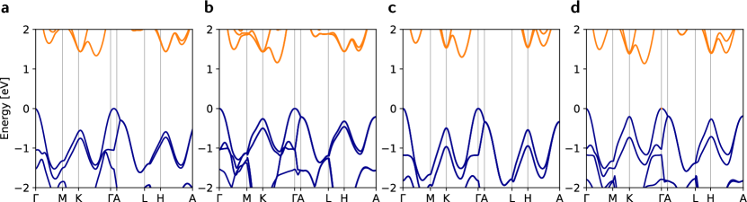
| X | XA | |||||
|---|---|---|---|---|---|---|
| \ceMoS2 | 1.34 | 1.99 | 0.20 | 1.846 | 1.877 | 0.031 |
| 1.14a | 1.82a | 0.16a | ||||
| \ceMoSe2 | 1.16 | 1.69 | 0.24 | 1.583 | 1.607 | 0.024 |
| 1.25a | 1.57a | 0.20a | ||||
| \ceWS2 | 1.30 | 2.02 | 0.47 | 1.915 | 1.956 | 0.041 |
| 1.25a | 1.82a | 0.44a | ||||
| \ceWSe2 | 1.14 | 1.59 | 0.49 | 1.511 | 1.561 | 0.050 |
| 1.12a | 1.62a | 0.48a |
a Ref. 46
Turning to the optical properties, the computed imaginary part of the dielectric function at both the independent particle (IP) level and including e-h interaction are shown in Fig. 3. For comparison, we also show the experimental optical absorption results (Refs. 47 and 48) for the respective TMDCs (shadow areas).
We notice a good agreement between the BSE optical spectra and the experimental ones, highlighting the excitons’ role in the optical absorption of bulk TMDCs. Overall, our findings effectively capture the essential characteristics of the experimental spectra, albeit with slightly diminished accuracy for W-based TMDCs primarily attributable to the increased splitting of electronic bands induced by higher spin-orbit coupling. The lack of prominent peaks in the IP spectrum strongly suggests that the sharp redshifted X peaks observed in BSE are associated with excitonic features. The absorption spectra calculated within IP exhibit noticeably weaker and less defined shoulder-like characteristics, indicating primarily band transitions. The two lowest energy peaks correspond to the excitonic states labeled as A and B, which are associated with interband transitions at the point in the Brillouin zone, coming from the splitting of the valence band due to spin-orbit coupling 49, 50.
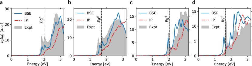
Our results indicate that the ground-state exciton (X) for all the studied systems corresponds to a dark state, that rises from transitions between the valence band maximum and conduction band minimum at the point. The corresponding excitonic peak energy position of X and XA for the TMDCs are summarized in Table 2.
Now we investigate the photovoltaic efficiency of the bulk TMDCs. Yu and Zunger 51 developed the so-called spectroscopic limited maximum efficiency (SLME) model to compute the maximum efficiency of the absorber in a single-junction solar cell. In this formalism, the magnitude of the fundamental band gap, the values of the direct and indirect electronic gaps, the standard solar spectrum, the absorption coefficient of the material, and the thickness are taken into account to estimate the PCE of the device
| (4) |
where is the total incident power density with a value of W/m2, and is the maximum output power density which can be obtained by maximizing the product of current density, , and voltage, ,
| (5) |
where is the Boltzmann constant, and is the device temperature taken as K throughout this work. Both the short circuit current density and the reverse saturation current density are calculated from the photon absorptivity of the material as follows
| (6) |
where is the absorption coefficient computed from first principles, and is the thickness of the photovoltaic absorber material taken as 500 nm unless otherwise stated. In this regard, those current densities can be described including the AM1.5G solar spectrum and the black-body spectrum , respectively
| (7) | |||||
| (8) |
corresponds to the total e-h recombination current at equilibrium in the dark, regarding both radiative and non-radiative recombinations. Here, is proposed as the fraction of the radiative recombination current, which in the original SLME framework is modeled using a Boltzmann factor
| (9) |
where is the difference between the allowed direct band gap and the fundamental band gap, respectively.
Note that the efficiency within the Shockley–Queisser (SQ) detailed balance limit 52 () can be obtained from the equations above by setting and considering the absorbance in Eq. (7) and (8) as a Heaviside step function that vanishes for and is equal to for , where is the optical band gap of the photovoltaic absorber.
| Shockley-Queisser | SLME | ||||||||
|---|---|---|---|---|---|---|---|---|---|
| mA/cm2 | (V) | FF (%) | (%) | mA/cm2 | (V) | FF (%) | (%) | ||
| \ceMoS2 | 17.5 | 1.55 | 92.2 | 25.0 | 17.5 | 1.02 | 88.6 | 15.8 | |
| \ceMoSe2 | 25.2 | 1.30 | 90.7 | 29.7 | 25.2 | 0.86 | 86.5 | 18.7 | |
| \ceWS2 | 15.6 | 1.63 | 91.8 | 23.3 | 15.6 | 0.98 | 87.4 | 13.4 | |
| \ceWSe2 | 26.9 | 1.26 | 90.1 | 30.5 | 26.9 | 0.84 | 86.4 | 19.5 | |
| SLME-X | SLME-PLQY | ||||||||
| mA/cm2 | (V) | FF (%) | (%) | mA/cm2 | (V) | FF (%) | (%) | ||
| \ceMoS2 | 17.5 | 1.52 | 92.0 | 24.5 | 17.5 | 1.31 | 90.5 | 20.8 | |
| \ceMoSe2 | 25.2 | 1.28 | 90.3 | 29.1 | 25.2 | 1.06 | 88.8 | 23.7 | |
| \ceWS2 | 15.6 | 1.59 | 91.6 | 22.7 | 15.6 | 1.37 | 91.1 | 19.4 | |
| \ceWSe2 | 26.9 | 1.21 | 89.8 | 29.2 | 26.9 | 1.01 | 88.1 | 23.8 | |
It is important to notice that for indirect band gap materials with large , as in the TMDCs studied here, the original SLME approach can drastically underestimate the predicted PCE, given that the Boltzmann factor rapidly decreases the fraction of radiative recombination current density . Consequently, the saturation current is overestimated, yielding lower values for the open-circuit voltages. This effect was studied in detail by Bercx et al. 54 for silicon, which possesses a eV. This leads to a PCE of zero regardless of the temperature and thickness of the material.
First, we apply the standard SLME formalism to compute the PCEs considering as the difference between and . Employing this approach, for all the analyzed systems, the fraction of radiative recombination current, , is much smaller than 10-8, leading to PCEs varying between 13% and 19% for the studied TMDCs, significantly smaller than those obtained through Shockley-Queisser (Table 3). This result suggests that, for these materials, employing the original SLME approach implies that almost all e-h recombination would be non-radiative, even though is modeled assuming a black-body spectrum, which relies on a radiative principle. This issue motivated us to explore alternative models for describing the recombination factor.
Delving into this possibility, and taking into account that the excitonic effects in bulk TMDCs play a key role in their optical responses, we also compute the PCE using a slightly modified SLME approach that has been proposed by Ozório and co-workers 30. In their model, the fraction of the radiative recombination current, , is calculated by replacing the in Eq. (9) with , which is defined as
| (10) |
We refer to this approach as exciton-based SLME or SLME-X. Within it, the fraction of the radiative recombination current, , calculated taking into account the values presented in Table 2. As a result, the obtained values vary between 1.510-2 and 3.910-2. It is important to point out that the presence of an indirect gap could lead to lower energy dark excitons that lead to non-radiative decay. Thus, the most effective method for obtaining the exciton ground state involves computing the -dependent BSE spectra 55. In that case, we expect that would have even lower values, although still surpassing those obtained within the standard SLME.
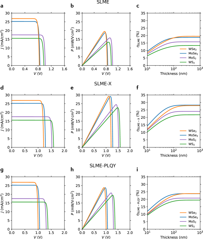
In Fig. 4a-b, we show the current and power density curves as a function of the voltage, obtained with the SLME-X approach. The PCE as a function of thickness is depicted in Fig. 4c. All the main solar cell parameters obtained from these curves are summarized in Table 3.
We can verify that all the investigated photovoltaic properties are similar for those TMDCs that are composed of the same chalcogen species. The transition metal diselenides should have higher photovoltaic efficiencies than disulfides due to their lower optical band gaps. In addition, our results presented in Fig. 4(c) indicate that saturates for a thickness around nm.
Alternatively, non-radiative recombination losses can be experimentally quantified by the photoluminescence quantum yield (PLQY) 56. We can also estimate the maximum PCE by assuming that the PLQY is, in principle, equal to the fraction of radiative recombination () 57. We denote this other modified SLME approach as SLME-PLQY. Experimental studies have reported that for single-layer TMDCs, the PLQY is close to unity 58, 59, 53. In contrast, it has been demonstrated that the PLQY for their bulk counterpart is reduced by a factor of 104 60.
We adopt the PLQY values reported by Mohamed and co-workers 53 as the experimental-based for the TMDCs. These values are 6.810-5, 7.910-5, 4.910-5, and 4.510-5 for the bulk \ceMoS2, \ceMoSe2, \ceWS2 and \ceWSe2, respectively.
Considering the SLME-PLQY approach, we also calculate the current density-voltage, power density-voltage, and PCE-thickness curves of the studied TMDCs, which are shown in Fig. 4d-f. For comparison with the SLME-X results, we describe the solar cell parameters obtained within SLME-PLQY for the TMDCs in Table 3. Given that the short-circuit current densities, , do not depend on the fraction of the radiative recombination current, their values are identical for both approaches. On the other hand, the open-circuit voltages and fill factors are smaller in the SLME-PLQY approach in comparison to the SLME-X one, leading to smaller values of PCE in the latter case.
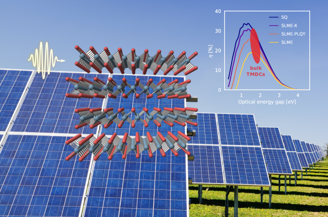
All the obtained results of the photovoltaic efficiencies within the SQ and SLME-based approaches are summarized in Fig. 5, where we present the maximum PCE as a function of the optical band gap. For the analyzed TMDCs, the average of the fraction of e-h radiative recombination is for the standard SLME, for SLME-PLQY and for SLME-X. In addition, we have estimated the error associated with those average maximum PCEs, by introducing in the the error threshold of the calculations (see Fig. S5 in the Supporting Information). As a result, regarding the SLME approach, for systems with optical gaps close to 1.9 eV (\ceMoS2, \ceWS2), the estimated error is 1%, whereas for those with optical gaps around 1.6 eV (\ceMoSe2, \ceWSe2), the error can be approximately 2.4%. Considering this uncertainty estimate, we expect comparable errors for the remaining formalisms.
Based on these fractions of non-radiative e-h recombination, we compute the efficiencies as a function of the optical energy gap. The shaded area in Fig. 5 represents the range of optical band gaps corresponding to the TMDCs studied. We can verify that the SQ formalism, which considers only radiative recombination processes (), overestimates the photovoltaic efficiency of the bulk TMDCs, with photovoltaic efficiencies ranging from % to % (Table S1 in the Supporting Information 42). On the other hand, all the SLME-based approaches include a non-vanishing fraction of non-radiative e-h recombination (), decreasing the predicted photovoltaic efficiencies of the absorbers.

Our results suggest that even the highest quality TMDC-based thin film would yield maximum efficiencies between %, if we take into account only excitonic effects as a fundamental factor to describe the recombination processes. Nevertheless, a more realistic upper limit of the photovoltaic efficiency for the investigated TMDCs can be predicted by considering the fraction of the radiative recombination directly from PLQY experiments, with the TMDC thin-films reaching maximum PCEs between %. Based on it, it is noticeable that PLQY-based efficiencies, reflecting the performance of impurity-containing samples, are inferior to those derived from considering only excitonic effects. This implies that there is still room for improving the TMDC samples to attain greater PCEs.
The obtained efficiencies can be compared with previous theoretical studies. For instance, Ozdemir and Baroni 61 investigated the photovoltaic efficiency of bulk TMDCs based on ab initio many-body perturbation theory calculations, including the e-h interaction. In their work, the absorptivity is calculated as , where is the transmitivity and is the reflectivity, and those properties are computed from Fresnel’s equations. For TMDCs with a thickness of nm, the same ones analyzed in our work, they reported values of PCE in a range of 21% to 26%, being the selenides the most efficient systems, consistent with our findings, especially those that account for nonradiative recombination through PLQY experiments.
Furthermore, Chouldhary et al. 62 have reported theoretical results of SLME based on DFT without taking e-h interactions into account. The computed for a thickness of 500 nm were , , , and for bulk \ceMoS2, \ceMoSe2, \ceWS2, and \ceWSe2, respectively. Although in that work the authors have used band gaps calculated at the DFT level with meta-GGA functionals, their SLME efficiencies lie between our predicted values modeled by the SLME-X and SLME-PLQY approaches.
Finally, despite the large range of efficiencies, we verify that the selenides present higher efficiencies, with \ceMoSe2 and \ceWSe2 photovoltaic efficiencies being almost the same. Our results highlight the importance of the fraction of radiative e-h recombination factor () to determine the maximum PCEs of bulk TMDCs, which indeed can be extrapolated to other indirect band gap absorbers. In particular, we present a range of values for this relevant solar cell parameter and their corresponding efficiencies, based on several approaches that can represent reliable upper limits for the photovoltaic efficiencies of single-junction solar devices produced with TMDC thin films.
4 Conclusions
We carried out first-principles calculations based on DFT combined with many-body perturbation theory within the -BSE framework to study the optical response and the photovoltaic properties of bulk 2H-\ceMX2 (MMo, W, and XS, Se), using for the latter the spectroscopic limited maximum efficiency (SLME) formalism. Our results indicated that an accurate description of the optical spectrum within the -BSE framework requires mapping out the Brillouin zone in very fine k-grid samples. The agreement obtained when comparing the BSE optical spectra and the experimental ones highlights the excitons’ roles in the optical absorption of bulk TMDCs. The calculated power conversion efficiencies (PCEs) of the analyzed TMDCs were overestimated with the Shockley-Queisser formalism, as expected since in this approach one includes only radiative e-h recombination losses. On the other hand, the standard SLME approach tends to underestimate the PCE of these van der Waals materials, due to a quite small estimate of the fraction of radiative recombination. In other words, for the standard SLME, almost all the recombination processes should correspond to nonradiative losses. These findings have motivated us to explore alternative methods for modeling PCEs that account for radiative and nonradiative recombination processes in more realistic ways. Thus, we investigate the modeling of the fraction of e-h recombination processes by considering the energy range from exciton eigenvalues (SLME-X), and also by employing experimental results obtained for photoluminescence quantum yield (SLME-PLQY). As a result, we predict that when we adopt the exciton energy ranges to compute the PCE within the SLME-X approach, the maximum PCEs vary between %, whereas taking the experimental fraction of radiative e-h recombination from PLQY experiments within the SLME-PLQY approach, the bulk TMDC maximum PCEs reached values between %. Regardless of the approach used to determine the PCE, our results indicate that the selenide-based TMDCs exhibit superior photovoltaic efficiency in comparison to the sulfide-based ones. In conclusion, we believe that our comprehensive analysis of the effects of the fraction of e-h radiative recombination in the TMDC efficiencies can be used as accurate predictions of upper limits for the photovoltaic efficiencies of solar devices based on few-layer or multi-layer TMDCs, paving the way for the development of efficient nanoscopically thin solar cells.
Acknowledgements
E.M.Jr and A.R.R. acknowledge the financial support from the Brazilian agency FAPESP, Grant No. 20/13172-8 and 2017/02317-2. This research was supported by resources supplied by CENAPAD-SP and the Center for Scientific Computing (NCC/GridUNESP) of the UNESP.
References
- Han 2020 Han, X. Ductile van der Waals materials. Science 2020, 369, 509–509
- Novoselov et al. 2004 Novoselov, K. S.; Geim, A. K.; Morozov, S. V.; Jiang, D.; Zhang, Y.; Dubonos, S. V.; Grigorieva, I. V.; Firsov, A. A. Electric Field Effect in Atomically Thin Carbon Films. Science 2004, 306, 666–669
- Khan et al. 2020 Khan, K.; Tareen, A. K.; Aslam, M.; Wang, R.; Zhang, Y.; Mahmood, A.; Ouyang, Z.; Zhang, H.; Guo, Z. Recent developments in emerging two-dimensional materials and their applications. J. Mater. Chem. C 2020, 8, 387–440
- Ma et al. 2021 Ma, Q.; Ren, G.; Xu, K.; Ou, J. Z. Tunable optical properties of 2D materials and their applications. Adv. Opt. Mater. 2021, 9, 2001313
- Villegas and Rocha 2022 Villegas, C. E. P.; Rocha, A. R. Near-Infrared Optical Response and Carrier Dynamics for High Photoconversion in Tellurene. J. Phys. Chem. C 2022, 126, 6129–6134
- Chhowalla et al. 2013 Chhowalla, M.; Shin, H. S.; Eda, G.; Li, L.-J.; Loh, K. P.; Zhang, H. The chemistry of two-dimensional layered transition metal dichalcogenide nanosheets. Nat. Chem. 2013, 5, 263–275
- Manzeli et al. 2017 Manzeli, S.; Ovchinnikov, D.; Pasquier, D.; Yazyev, O. V.; Kis, A. 2D transition metal dichalcogenides. Nat. Rev. Mater. 2017, 2, 17033–15
- Perez et al. 2020 Perez, A.; Amorim, R. G.; Villegas, C. E. P.; Rocha, A. R. Nanogap-based all-electronic DNA sequencing devices using MoS 2 monolayers. Phys. Chem. Chem. Phys. 2020, 22, 27053–27059
- Villegas and Rocha 2015 Villegas, C. E. P.; Rocha, A. R. Elucidating the optical properties of novel heterolayered materials based on MoTe2–InN for photovoltaic applications. J. Phys. Chem. C 2015, 119, 11886–11895
- Britnell et al. 2013 Britnell, L.; Ribeiro, R. M.; Eckmann, A.; Jalil, R.; Belle, B. D.; Mishchenko, A.; Kim, Y.-J.; Gorbachev, R. V.; Georgiou, T.; Morozov, S. V.; Grigorenko, A. N.; Geim, A. K.; Casiraghi, C.; Neto, A. H. C.; Novoselov, K. S. Strong Light-Matter Interactions in Heterostructures of Atomically Thin Films. Science 2013, 340, 1311–1314
- Furchi et al. 2018 Furchi, M. M.; Höller, F.; Dobusch, L.; Polyushkin, D. K.; Schuler, S.; Mueller, T. Device physics of van der Waals heterojunction solar cells. npj 2D Mater. Appl. 2018, 2, 3
- Baugher et al. 2014 Baugher, B. W.; Churchill, H. O.; Yang, Y.; Jarillo-Herrero, P. Optoelectronic devices based on electrically tunable p–n diodes in a monolayer dichalcogenide. Nat. Nanotechnol. 2014, 9, 262–267
- Kim and Choi 2021 Kim, H. G.; Choi, H. J. Thickness dependence of work function, ionization energy, and electron affinity of Mo and W dichalcogenides from DFT and GW calculations. Phys. Rev. B 2021, 103, 1–9
- Aftab et al. 2023 Aftab, S.; Iqbal, M. Z.; Hussain, S.; Hegazy, H. H.; Saeed, M. A. Transition metal dichalcogenides solar cells and integration with perovskites. Nano Energy 2023, 108, 108249
- Nassiri Nazif et al. 2021 Nassiri Nazif, K.; Kumar, A.; Hong, J.; Lee, N.; Islam, R.; McClellan, C. J.; Karni, O.; van de Groep, J.; Heinz, T. F.; Pop, E.; Brongersma, M. L.; Saraswat, K. C. High-performance p–n junction transition metal dichalcogenide photovoltaic cells enabled by MoO x doping and passivation. Nano Lett. 2021, 21, 3443–3450
- He et al. 2022 He, X.; Iwamoto, Y.; Kaneko, T.; Kato, T. Fabrication of near-invisible solar cell with monolayer WS2. Sci. Rep. 2022, 12, 11315
- Bernardi et al. 2013 Bernardi, M.; Palummo, M.; Grossman, J. C. Extraordinary Sunlight Absorption and One Nanometer Thick Photovoltaics Using Two-Dimensional Monolayer Materials. Nano Lett. 2013, 13, 3664–3670
- Britnell et al. 2013 Britnell, L.; Ribeiro, R. M.; Eckmann, A.; Jalil, R.; Belle, B. D.; Mishchenko, A.; Kim, Y.-J.; Gorbachev, R. V.; Georgiou, T.; Morozov, S. V.; Grigorenko, A. N.; Geim, A. K.; Casiraghi, C.; Neto, A. H. C.; Novoselov, K. S. Strong light-matter interactions in heterostructures of atomically thin films. Science 2013, 340, 1311–1314
- Li et al. 2015 Li, H.-M.; Lee, D.; Qu, D.; Liu, X.; Ryu, J.; Seabaugh, A.; Yoo, W. J. Ultimate thin vertical p–n junction composed of two-dimensional layered molybdenum disulfide. Nat. Comm. 2015, 6, 6564
- Cheng et al. 2014 Cheng, R.; Li, D.; Zhou, H.; Wang, C.; Yin, A.; Jiang, S.; Liu, Y.; Chen, Y.; Huang, Y.; Duan, X. Electroluminescence and Photocurrent Generation from Atomically Sharp WSe2/MoS2 Heterojunction p–n Diodes. Nano Lett. 2014, 14, 5590–5597
- Mao et al. 2018 Mao, X.; Zou, J.; Li, H.; Song, Z.; He, S. Magnetron sputtering fabrication and photoelectric properties of WSe2 film solar cell device. Appl. Surf. Sci. 2018, 444, 126–132
- Went et al. 2019 Went, C. M.; Wong, J.; Jahelka, P. R.; Kelzenberg, M.; Biswas, S.; Hunt, M. S.; Carbone, A.; Atwater, H. A. A new metal transfer process for van der Waals contacts to vertical Schottky-junction transition metal dichalcogenide photovoltaics. Sci. Adv. 2019, 5, eaax6061
- McVay et al. 2020 McVay, E.; Zubair, A.; Lin, Y.; Nourbakhsh, A.; Palacios, T. Impact of Al2O3 passivation on the photovoltaic performance of vertical WSe2 Schottky junction solar cells. ACS Appl. Mater. Interfaces 2020, 12, 57987–57995
- Islam et al. 2022 Islam, K. M.; Ismael, T.; Luthy, C.; Kizilkaya, O.; Escarra, M. D. Large-Area, High-Specific-Power Schottky-Junction Photovoltaics from CVD-Grown Monolayer MoS2. ACS Applied Materials & Interfaces 2022, 14, 24281–24289
- Liu et al. 2018 Liu, Y.; Guo, J.; Zhu, E.; Liao, L.; Lee, S.-J.; Ding, M.; Shakir, I.; Gambin, V.; Huang, Y.; Duan, X. Approaching the Schottky–Mott limit in van der Waals metal–semiconductor junctions. Nature 2018, 557, 696–700
- Lee et al. 2014 Lee, C.-H.; Lee, G.-H.; van der Zande, A. M.; Chen, W.; Li, Y.; Han, M.; Cui, X.; Arefe, G.; Nuckolls, C.; Heinz, T. F.; Guo, J.; Hone, J.; Kim, P. Atomically thin p–n junctions with van der Waals heterointerfaces. Nat. Nanotechnol. 2014, 9, 676–681
- Memaran et al. 2015 Memaran, S.; Pradhan, N. R.; Lu, Z.; Rhodes, D.; Ludwig, J.; Zhou, Q.; Ogunsolu, O.; Ajayan, P. M.; Smirnov, D.; Fernández-Domínguez, A. I.; García-Vidal, F. J.; Balicas, L. Pronounced photovoltaic response from multilayered transition-metal dichalcogenides PN-junctions. Nano Lett. 2015, 15, 7532–7538
- Cho et al. 2018 Cho, A.-J.; Song, M.-K.; Kang, D.-W.; Kwon, J.-Y. Two-Dimensional WSe2/MoS2 p–n Heterojunction-Based Transparent Photovoltaic Cell and Its Performance Enhancement by Fluoropolymer Passivation. ACS Appl. Mater. Interfaces 2018, 10, 35972–35977
- Nassiri Nazif et al. 2021 Nassiri Nazif, K.; Daus, A.; Hong, J.; Lee, N.; Vaziri, S.; Kumar, A.; Nitta, F.; Chen, M. E.; Kananian, S.; Islam, R.; Kim, K.-H.; Park, J.-H.; Poon, A. S. Y.; Brongersma, M. L.; Pop, E.; Saraswat, K. C. High-specific-power flexible transition metal dichalcogenide solar cells. Nat. Commun. 2021, 12, 7034
- Ozório et al. 2022 Ozório, M. S.; Dias, A. C.; Silveira, J. F.; Da Silva, J. L. Theoretical Investigation of the Role of Anion and Trivalent Cation Substitution in the Physical Properties of Lead-Free Zero-Dimensional Perovskites. J. Phys. Chem. C 2022, 126, 7245–7255
- Hohenberg and Kohn 1964 Hohenberg, P.; Kohn, W. Inhomogeneous electron gas. Phys. Rev. 1964, 136, B864
- Kohn and Sham 1965 Kohn, W.; Sham, L. J. Self-consistent equations including exchange and correlation effects. Phys. Rev. 1965, 140, A1133
- Giannozzi et al. 2009 Giannozzi, P.; Baroni, S.; Bonini, N.; Calandra, M.; Car, R.; Cavazzoni, C.; Ceresoli, D.; Chiarotti, G. L.; Cococcioni, M.; Dabo, I.; Corso, A. D.; de Gironcoli, S.; Fabris, S.; Fratesi, G.; Gebauer, R.; Gerstmann, U.; Gougoussis, C.; Kokalj, A.; Lazzeri, M.; Martin-Samos, L.; Marzari, N.; Mauri, F.; Mazzarello, R.; Paolini, S.; Pasquarello, A.; Paulatto, L.; Sbraccia, C.; Scandolo, S.; Sclauzero, G.; Seitsonen, A. P.; Smogunov, A.; Umari, P.; Wentzcovitch, R. M. QUANTUM ESPRESSO: a modular and open-source software project for quantum simulations of materials. J. Phys.: Condens. Matter 2009, 21, 395502
- Perdew et al. 1996 Perdew, J. P.; Burke, K.; Ernzerhof, M. Generalized gradient approximation made simple. Phys. Rev. Lett. 1996, 77, 3865
- Hamann 2013 Hamann, D. R. Optimized norm-conserving Vanderbilt pseudopotentials. Phys. Rev. B 2013, 88, 085117
- Grimme 2006 Grimme, S. Semiempirical GGA-type density functional constructed with a long-range dispersion correction. J. Comput. Chem. 2006, 27, 1787–1799
- Hedin 1965 Hedin, L. New Method for Calculating the One-Particle Green’s Function with Application to the Electron-Gas Problem. Phys. Rev. 1965, 139, A796–A823
- Marini et al. 2009 Marini, A.; Hogan, C.; Grüning, M.; Varsano, D. yambo: An ab initio tool for excited state calculations. Comput. Phys. Commun. 2009, 180, 1392–1403
- Bruneval and Gonze 2008 Bruneval, F.; Gonze, X. Accurate self-energies in a plane-wave basis using only a few empty states: Towards large systems. Phys. Rev. B 2008, 78, 085125
- Rohlfing and Louie 2000 Rohlfing, M.; Louie, S. G. Electron-hole excitations and optical spectra from first principles. Phys. Rev. B 2000, 62, 4927–4944
- Kammerlander et al. 2012 Kammerlander, D.; Botti, S.; Marques, M. A.; Marini, A.; Attaccalite, C. Speeding up the solution of the Bethe-Salpeter equation by a double-grid method and Wannier interpolation. Phys. Rev. B 2012, 86, 125203
- 42 Supporting information: convergence analyses of and BSE calculations, and results of photovoltaic properties of the bulk TMDCs within Shockley-Queisser formalism.
- Wildervanck and Jellinek 1964 Wildervanck, J.; Jellinek, F. Preparation and crystallinity of molybdenum and tungsten sulfides. Z. Anorg. Allg. Chem. 1964, 328, 309
- Schutte et al. 1987 Schutte, W.; De Boer, J.; Jellinek, F. Crystal structures of tungsten disulfide and diselenide. J. Solid State Chem. 1987, 70, 207–209
- Evans and Hazelwood 1971 Evans, B.; Hazelwood, R. Optical and structural properties of MoSe2. Phys. Status Solidi (A) 1971, 4, 181
- Kim et al. 2016 Kim, B. S.; Rhim, J.-W.; Kim, B.; Kim, C.; Park, S. R. Determination of the band parameters of bulk 2H-MX2 (M= Mo, W; X= S, Se) by angle-resolved photoemission spectroscopy. Sci. Rep. 2016, 6, 36389
- Beal et al. 1976 Beal, A.; Liang, W.; Hughes, H. Kramers-Kronig analysis of the reflectivity spectra of 3R-WS2 and 2H-WSe2. J. Phys. C: Solid State Phys. 1976, 9, 2449
- Beal and Hughes 1979 Beal, A.; Hughes, H. Kramers-Kronig analysis of the reflectivity spectra of 2H-MoS2, 2H-MoSe2 and 2H-MoTe2. J. Phys. C: Solid State Phys. 1979, 12, 881
- Li et al. 2014 Li, Y.; Chernikov, A.; Zhang, X.; Rigosi, A.; Hill, H. M.; Van Der Zande, A. M.; Chenet, D. A.; Shih, E.-M.; Hone, J.; Heinz, T. F. Measurement of the optical dielectric function of monolayer transition-metal dichalcogenides: MoS 2, Mo S e 2, WS 2, and WS e 2. Phys. Rev. B 2014, 90, 205422
- Wang et al. 2018 Wang, G.; Chernikov, A.; Glazov, M. M.; Heinz, T. F.; Marie, X.; Amand, T.; Urbaszek, B. Colloquium: Excitons in atomically thin transition metal dichalcogenides. Rev. Mod. Phys. 2018, 90, 021001
- Yu and Zunger 2012 Yu, L.; Zunger, A. Identification of Potential Photovoltaic Absorbers Based on First-Principles Spectroscopic Screening of Materials. Phys. Rev. Lett. 2012, 108, 068701
- Shockley and Queisser 1961 Shockley, W.; Queisser, H. J. Detailed Balance Limit of Efficiency of p-n Junction Solar Cells. J. Appl. Phys. 1961, 32, 510–519
- Mohamed et al. 2017 Mohamed, N. B.; Lim, H. E.; Wang, F.; Koirala, S.; Mouri, S.; Shinokita, K.; Miyauchi, Y.; Matsuda, K. Long radiative lifetimes of excitons in monolayer transition-metal dichalcogenides MX2 (M= Mo, W; X= S, Se). Appl. Phys. Express 2017, 11, 015201
- Bercx et al. 2016 Bercx, M.; Sarmadian, N.; Saniz, R.; Partoens, B.; Lamoen, D. First-principles analysis of the spectroscopic limited maximum efficiency of photovoltaic absorber layers for CuAu-like chalcogenides and silicon. Phys. Chem. Chem. Phys. 2016, 18, 20542–20549
- Moujaes and Dias 2023 Moujaes, E. A.; Dias, A. C. On the excitonic effects of the 1T and 1OT phases of PdS2, PdSe2, and PdSSe monolayers. J. Phys. Chem. Solids 2023, 182, 111573
- Dreessen et al. 2023 Dreessen, C.; Zanoni, K. P. S.; Gil-Escrig, L.; Rodkey, N.; Khan, J. I.; Laquai, F.; Sessolo, M.; Roldán-Carmona, C.; Bolink, H. J. When JV Curves Conceal Material Improvements: The Relevance of Photoluminescence Measurements in the Optimization of Perovskite Solar Cells. Adv. Opt. Mater. 2023, n/a, 2301019
- Jariwala et al. 2017 Jariwala, D.; Davoyan, A. R.; Wong, J.; Atwater, H. A. Van der Waals materials for atomically-thin photovoltaics: promise and outlook. ACS Photonics 2017, 4, 2962–2970
- Amani et al. 2015 Amani, M.; Lien, D.-H.; Kiriya, D.; Xiao, J.; Azcatl, A.; Noh, J.; Madhvapathy, S. R.; Addou, R.; KC, S.; Dubey, M.; Cho, K.; Wallace, R. M.; Lee, S.-C.; He, J.-H.; Ager, J. W.; Zhang, X.; Yablonovitch, E.; Javey, A. Near-unity photoluminescence quantum yield in MoS2. Science 2015, 350, 1065–1068
- Amani et al. 2016 Amani, M.; Taheri, P.; Addou, R.; Ahn, G. H.; Kiriya, D.; Lien, D.-H.; Ager III, J. W.; Wallace, R. M.; Javey, A. Recombination kinetics and effects of superacid treatment in sulfur-and selenium-based transition metal dichalcogenides. Nano Lett. 2016, 16, 2786–2791
- Mak et al. 2010 Mak, K. F.; Lee, C.; Hone, J.; Shan, J.; Heinz, T. F. Atomically thin MoS 2: a new direct-gap semiconductor. Phys. Rev. Lett. 2010, 105, 136805
- Ozdemir and Barone 2020 Ozdemir, B.; Barone, V. Thickness dependence of solar cell efficiency in transition metal dichalcogenides MX2 (M: Mo, W; X: S, Se, Te). Sol. Energy Mater Sol. Cells 2020, 212, 110557
- Choudhary et al. 2019 Choudhary, K.; Bercx, M.; Jiang, J.; Pachter, R.; Lamoen, D.; Tavazza, F. Accelerated discovery of efficient solar cell materials using quantum and machine-learning methods. Chem. Mater. 2019, 31, 5900–5908
TOC Graphic