Signature of pressure-induced topological phase transition in ZrTe5
Abstract
The layered van der Waals material ZrTe5 is known as a candidate topological insulator (TI), however its topological phase and the relation with other properties such as an apparent Dirac semimetallic state is still a subject of debate. We employ a semiclassical multicarrier transport (MCT) model to analyze the magnetotransport of ZrTe5 nanodevices at hydrostatic pressures up to 2 GPa. The temperature dependence of the MCT results between 10 and 300 K is assessed in the context of thermal activation, and we obtain the positions of conduction and valence band edges in the vicinity of the chemical potential. We find evidence of the closing and subsequent re-opening of the band gap with increasing pressure, which is consistent with a phase transition from weak to strong TI. This matches expectations from ab initio band structure calculations, as well as previous observations that CVT-grown ZrTe5 is in a weak TI phase in ambient conditions.
I Introduction
In certain materials, the spin-orbit interaction, through a process of band inversion, leads to a topological insulator (TI) phase [1, 2]. The most remarkable consequence of this phase is that despite being gapped in the bulk, any boundary between a TI and a trivial (non-topological) insulator features gapless edge or surface states. These topological edge states are of interest in the area of quantum computation [3]. In a two-dimensional (2D) case, this phase is also called a quantum spin Hall insulator. Initially, its existence had been proposed [4, 5] and then successfully demonstrated in HgTe/CdTe quantum wells [6, 7]. In addition, 3D TIs have also been discovered, initially with Bi2Se3 and Bi2Te3 at the forefront [8, 9]. These materials feature 2D surface states that have a chiral spin texture, where any orientation of the momentum uniquely determines the spin polarization, also called spin-momentum locking (SML) [10, 11, 12]. These chiral surface states are of interest for spintronics, since the SML mechanism can be taken advantage of, for example in heterostructures, to generate spin polarization and pass it into a spin transport medium such as graphene, or to electrically detect the presence of spin currents in the medium [13, 14, 15].
Zirconium pentatelluride (ZrTe5) is a 2D layered material [16] and features an anomalous resistivity peak at a sample-dependent temperature [17, 18]. This peak has been elucidated by angle-resolved photoemission spectroscopy (ARPES) [19, 20] to be caused by a shift of the chemical potential across the small band gap with temperature, while the predominant carriers change from holes to electrons as the temperature is reduced. In samples grown by chemical vapor transport (CVT), is typically in the K range [21, 22, 23], allowing for study of both electron and hole transport properties based on temperature.
ZrTe5 is a candidate TI [24], with the monolayer expected to form a quantum spin Hall insulator. The multilayer structure could be in a weak TI (WTI) or strong TI (STI) state, depending on the invariant [2, 10]. The WTI case has surface states present only on certain boundaries, essentially acting like a stack of 2D TIs, while the STI case has topologically protected surface states on all boundaries, forming a genuinely 3D TI, as depicted in Fig. 1 (b) and (d), respectively. However, whether it forms a WTI or STI is under debate [24, 25, 26, 27]. Certain experimental evidence suggests an STI phase [28, 29, 30]. However, most experiments have found CVT-grown ZrTe5 to be a WTI with a smaller band gap [19, 26, 31, 32], including observations using ARPES [33] and scanning tunneling microscopy [34, 35].
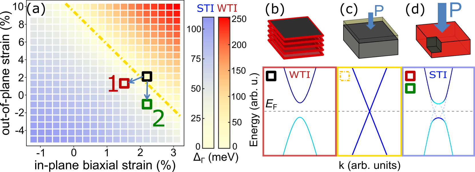
Theoretical band structure calculations generally predict a STI phase for ZrTe5 and show the presence of several distinct band edges near the Fermi level [24, 19, 25], supporting a multicarrier approach in the analysis of transport behavior. In addition, a few works consider it a Dirac or Weyl semimetal instead [36, 37, 38, 39]. The theoretical predictions and experimental observations generally agree that ZrTe5 lies close to a WTI-STI phase transition boundary (yellow line in Fig. 1 (a)), with only a small band gap in the Dirac-like bands, potentially allowing for observation of relativistic behavior. In addition, the band structure is highly sensitive to small changes in lattice constants [40]. The goal of this work was to investigate whether this property could be exploited, by application of pressure, to drive the material through this phase transition.
Application of hydrostatic pressure is an emerging tool of interest in the study of 2D materials and heterostructures, with practical experimental methods currently in development [41, 42]. The interlayer spacing is an important parameter, expected to tune properties of layered materials [43, 44] (including ZrTe5 [24, 25]) and heterostructures [45, 46]. Recently this tunability has been experimentally demonstrated in examples such as superconductivity in superlattices [41], band structure tuning of twisted bilayer graphene [47, 48], enhancement of spin-orbit proximity effects [49, 50] or magnetic ordering transitions [51].
Although a few studies have been performed on bulk ZrTe5 with application of pressure or strain [52, 53, 54, 23] (including regarding its phase transition [26]), experiments on thin nanodevices, where surface contributions are more evident in transport measurements, have not been performed before. The joint experimental and theoretical approach of this work is able to better reveal the signatures of this topological phase transition in ZrTe5 nanoflakes.
II Theoretical Calculations and Methods
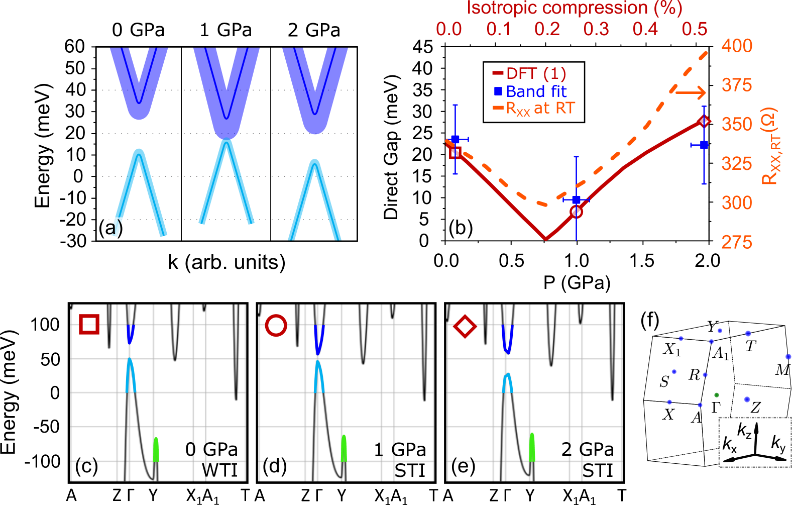
First, in order to assess the topological phase of ZrTe5 as a function of changes to lattice constants, and to help interpret the experimental results, we have performed ab initio band structure calculations, employing density functional theory (DFT). The size of the direct gap at the point, , is plotted as a function of in-plane and out-of-plane strain in Fig. 1 (a). The phase transition, where , is found along the yellow dash-dotted line. The topological phase of the system is found to be in a WTI phase above this line and an STI phase below it. The relaxed lattice constants are = 2.002 Å, = 7.204 Å and = 13.876 Å [40], representing the zero strain position on the strain map. These parameters fall within 1.1% of those obtained from X-ray diffraction [16]. It is important to note that the DFT-based band structure obtained using the relaxed constants does not accurately represent the experimental ZrTe5 results on CVT-grown crystals, instead predicting a larger band gap (around 80 meV), and, most notably, resulting in a STI rather than WTI phase. According to Ref. [55], the experimentally estimated ZrTe5 bands are better represented by the DFT results at the black square in Fig. 1 (a), which is close to the phase transition boundary and consistent with the experimental results of Refs. [19, 26, 31, 32, 33, 34, 35] suggesting a WTI phase.
A visual representation of the vicinity of the point for the WTI phase is shown on the lower part of Fig. 1 (b), having a trivial gap without band inversion for the 3D band structure. In this state, the edge states of the WTI phase run along the edges of the individual ZrTe5 layers, essentially each of them forming a 2D topological insulator, as is shown in the upper part of panel (b). Because this position is close to the gapless phase transition point, application of pressure is expected to compress the lattice and move the system through the phase transition and into an STI phase. The exact compression path is hard to predict, but the expectation from hydrostatic compression would be a movement from upper right to lower left of Fig. 1 (a) (arrows). For visualization, two example paths are chosen, labeled as 1 (2) showing an isotropic (vdW-only) compression process leading to an end position depicted as the red (green) square, respectively. Under the compression process, at a particular pressure value , the material would reach the transition point depicted in Fig. 1 (c), where the gap between the Dirac-like bands closes. Note that the overall band structure often has zero indirect gap, even away from the phase transition point, due to the multiple side bands being close to the chemical potential. For this reason, it is important to be able to assess the direct gap related to the topological phase transition. Further increasing the pressure would move the material into the STI phase, represented in Fig. 1 (d). Here, a band gap opens up again, but in this case the spin-orbit interaction leads to band inversion, highlighted by the coloring near the band edges. Gapless surface states will be found crossing this gap at every boundary (surface) of the crystal. Therefore, an experimental observation of closing and reopening can be considered as a signature of the topological phase transition.
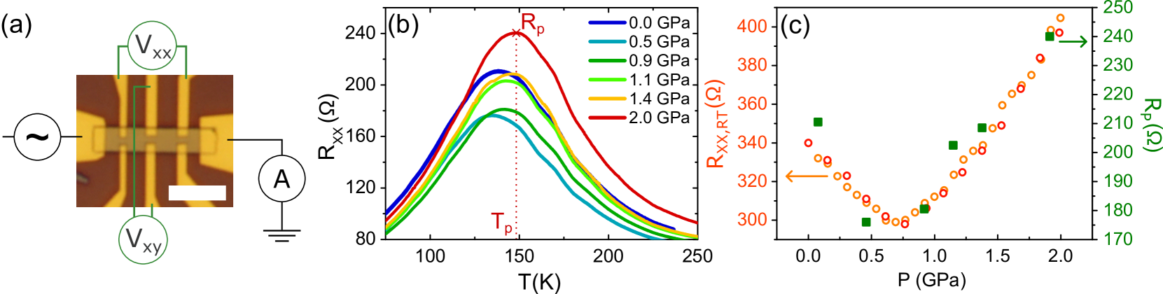
For experimental investigation under pressure, nanoflakes of ZrTe5 have been obtained by mechanical exfoliation to a SiO2 substrate. Predominantly, flakes in the nm thickness range have been studied, but measurements have also been performed on flakes thinner than 50 nm to study thickness dependence. The ZrTe5 crystals favorably cleave into regular rectangular single crystals of several m dimensions, where the longer edge of the exfoliated crystals is parallel to the crystallographic -axis [38, 56]. This allows for easy establishment of Hall-bar measurement geometries on the flakes by depositing metallic contacts. We have used electron beam lithography, with a Cr adhesion layer of 10 nm followed by a main Au layer of nm. To prepare a cleaner contact surface between ZrTe5 and the metal, an Ar ion beam milling step was performed immediately before deposition. A novel method for measuring nanodevices-on-chip under hydrostatic pressure was employed [42], in a piston-cylinder pressure cell that fits into the variable temperature insert of a liquid helium cyrostat with superconducting magnet (with fields up to 8 T), allowing for a full range ( K) of temperature-dependent magnetotransport measurements at pressures up to 2 GPa.
A multicarrier transport (MCT) approach was used to analyze the magnetotransport measurements and obtain band structure details under pressure. We have obtained the sheet conductivity data and from longitudinal and Hall resistance and measured in an out-of-plane magnetic field. Following Ref. [55], the obtained sheet conductivity data at each temperature was fitted using the MCT model, using signed conductivity and mobility as the fitting parameters for the i-th carrier, with the following equations:
| (1) |
The appropriate number of carriers (NC) is determined independently at each temperature, typically varying from along the full temperature range, with the highest number being necessary near the anomalous resistivity peak , where the chemical potential is crossing the small band gap. As shown in Ref. [55], one of the carriers (by convention ) is an edge-confined carrier, which runs only along the side edges of the ZrTe5 crystal and is thus unaffected by a field. It is implemented by setting its to a finite value while having , resulting in a constant, field-independent contribution to , and zero . This edge carrier is necessary to obtain smooth and realistic temperature trends for the densities and mobilities of all carriers. For all carriers other than this edge carrier, the relation applies, where is the 2D density of the -th carrier and is its charge. Dividing the 2D carrier density with crystal thickness results in the 3D carrier density .
Since in ZrTe5 the chemical potential crosses the band gap with temperature, the obtained data of the individual carriers can be used to fit a model band edge corresponding to the carrier, which has the form:
| (2) |
where is the density of states (DOS) of a band having the band edge energy and effective mass , assuming a 3D isotropic and quadratic band near the band edge. is the Fermi function with a temperature-dependent chemical potential, which is shifted with a rate meV/K with temperature (from Ref. [19]). We note that, similarly to Ref. [55], for the two high-mobility carriers (which we attribute to the ZrTe5 bands near ) we have used a 3D Dirac DOS for the fitting, with the Fermi velocity taking the place of . Most importantly, this method allows for the extraction of the band gap from the magnetotransport data, by subtracting the obtained band edge energies of the conduction and valence bands represented by these two carriers.
III Experimental Results and Discussion
Transport measurements on ZrTe5 nanoflakes, including application of pressure, were successfully performed on six devices in the nm thickness range, all of which behaved consistently. Here we discuss the results on two example devices; data on the others is shown in the Supporting Information (see Fig. S1). The measurement setup is shown in Fig. 2 (a), where the ZrTe5 crystallographic -axis is oriented horizontally on the image. A bias current was applied and simultaneous longitudinal and transverse measurements were taken. The temperature dependence of , the longitudinal resistance of device S1 (approx. 155 nm thick), is plotted at different pressures in Fig. 2 (b). The characteristic resistivity peak of ZrTe5 is observed to change with pressure, with both the resistance magnitude and its temperature position changing non-monotonically, first showing a decrease and then a subsequent increase with application of pressure. Previous measurements on bulk ZrTe5 crystals have shown nonmonotonic strain or pressure dependence as well [26, 23]. In Fig. 2 (c) the extracted dependence is shown as green squares. Though temperature dependent measurements can only be performed at a static pressure, which is set at room temperature (RT), we were able to measure the RT sample resistance dynamically during pressure application or release. This is plotted as the orange datapoints in Fig. 2 (c), and follows the dependence trend (green squares) well. This RT pressure dependence of is robust and reproducible across all samples, with a distinguishable minimum around 0.7 GPa.
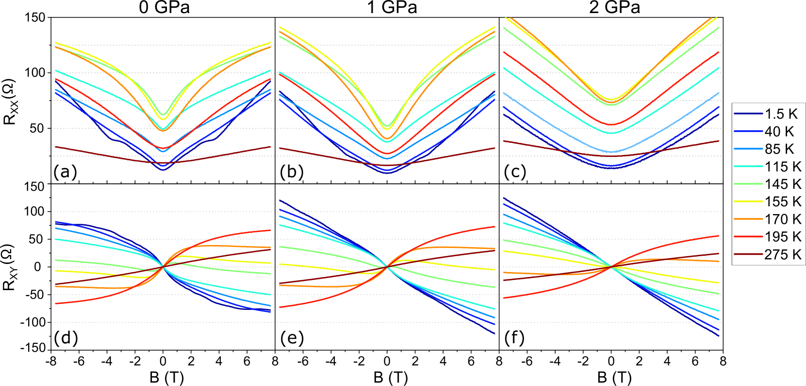
In order to employ the MCT method and obtain band structure details under pressure, magnetotransport measurements were performed. Fig. 3 shows a subset of the measurements in the K range on device S2 (approx. 98 nm thick) at pressures of approximately 0, 1 and 2 GPa respectively. Since the pressure medium freezes in the studied temperature range, the pressure decreases by roughly 0.1 GPa between 300 and 1.5 K when having a RT starting pressure above 1 GPa [57]. Therefore we consider 0.1 GPa as the uncertainty value. The and data have been symmetrized and anti-symmetrized, respectively. The 0 GPa dataset features the typical complex magnetotransport behavior of CVT-grown ZrTe5 [58, 59, 22, 55], with S-like shapes in originating from the the multiple carriers involved in transport. The gradual transition from valence to conduction band with decreasing temperature can be seen in the sign reversal of the predominant slope of . There is a noticeable effect with increasing pressure, which can be described as an apparent ”flattening” and simplification of both and curves at most temperatures. For example, the yellow curves (close to ) in Fig. 3 (d)-(f) initially have a slope reversal at low field, but this vanishes at 2 GPa and the slope is negative throughout. A notable change in the low temperature (blue) curves is that their hyperbolic-tangent-like shape at 0 GPa becomes almost completely linear at a pressure of 2 GPa. In addition, the weakening of Shubnikov-de Haas oscillations with increasing pressure can be observed in in Fig. 3 (a)-(c) (dark blue K curves). Overall, the curves at most temperatures, but especially near , feature a prominent symmetric dip at low pressure (panel (a)), and become closer to a parabolic- or V-shape under high pressure (panel (c)).
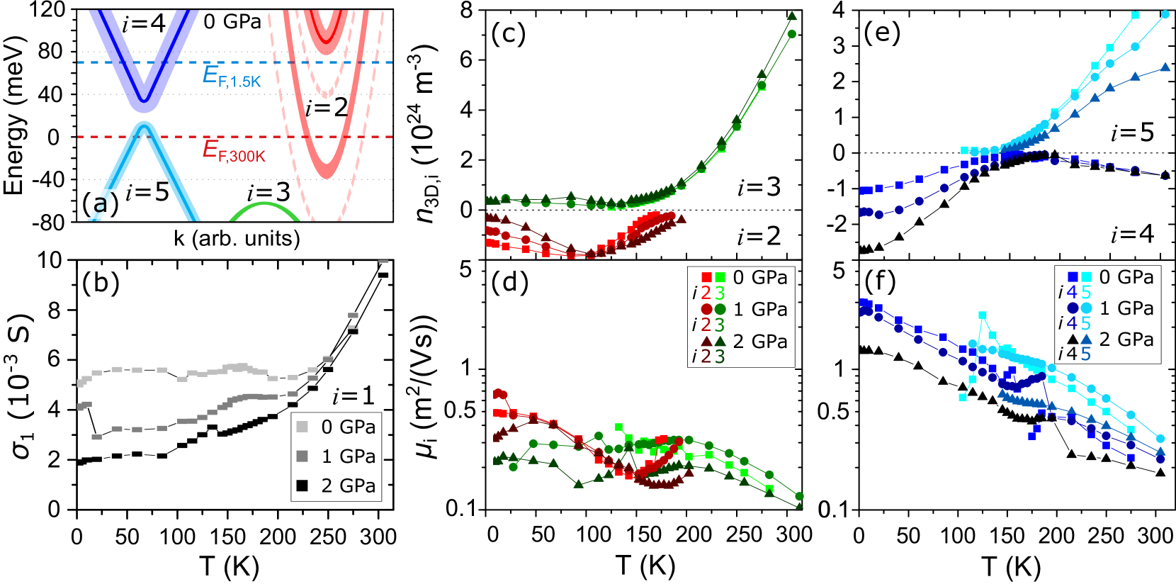
Following the methodology of Ref. [55], the magnetotransport curves from Fig. 3 can be fitted with the MCT model (Eqs. 1), with results of this fitting being shown in Fig. 4. The signed carrier density () trends with temperature are plotted for the low-mobility (, panel (c)) and high-mobility (, panel (e)) carriers. The corresponding mobilities () are plotted below, in Fig. 4 (d) and (f), respectively. It can be seen that each panel features an electron type (, with ) and a hole type (, with ) carrier, with the dominant carrier type changing near . This is most easily visible in panel (e) corresponding to the high-mobility Dirac-like bands near . A notable pressure dependence can be seen in this high-mobility pair. For the hole type carrier (), visible at higher temperatures, we observe a decrease of its amplitude with pressure. Meanwhile, the electron carrier (), which becomes relevant at lower temperatures, shows the opposite, an increase in the density with pressure. The contribution of edge-confined carrier is shown in Fig. 4 (b), exhibiting a notable decrease with increasing pressure. This carrier has no associated mobility value.
Fitting of the data using Eq. 2 results in the band edge energies , where most importantly the difference of the two high-mobility bands () can be used to get an estimate for . The final extracted band edge energies of the obtained bands at 0 GPa, relative to the chemical potential at 300 K, are represented in Fig. 4 (a). The darker, thin colored lines show the band edges attributed to each carrier, and the thicker, lighter colors represent the error of the fit. Note that for the carrier there are two solid bands drawn, because, according to the fitting procedure, this band shifts faster with temperature than the others. Therefore, the upper red band shows its starting position at 300 K while the lower band shows its final position at low temperature. This result is similar to the ARPES results of Ref. [19], showing an electron pocket along the A1-T high symmetry line shifting at a higher rate with temperature. The dashed red bands represent the error of the shift rate, marking the minima and maxima of the final band position at 1.5 K. The other bands in our results shift at a rate of 0.25 meV/K (according to Ref. [19]), which is already represented by the shift in Fig. 4 (a). Apart from an offset (which could be explained by n-doping), the obtained band edges are in good agreement with the DFT-based band structure from the black square position in Fig. 1 (a), see also Fig. 5 (c).
The pressure dependence of the gapped structure at is represented in Fig. 5 (a), showing the band edges attributed to the and carriers. The extracted gap size , and its error, are shown in the plot of Fig. 5 (b) as blue squares. The pressure evolution of the gap shows a decrease and subsequent increase, as would be expected from passing a WTI-to-STI phase transition. The tendency of the resistivity with pressure (measured at RT) is shown as the orange dashed line on the same plot, with a notable minimum. We suspect that this minimum, along with a similar minimum in and overall temperature-dependent resistivity (see Fig. 2), is an indication of the topological phase transition. The gapless state would therefore correspond to the position of this minimum, while opening a gap on either side of the phase transition would lead to an increase in resistivity. This is expected even more so at temperatures above , where the chemical potential is still in the valence band, and transport contributions due to thermal excitations across the gap are relevant. This would explain the observed non-monotonic pressure dependence. To verify the evolution of the gap size with pressure using the DFT-based calculations, we have extracted the gap size along the isotropic pressure path from Fig. 1 (a), plotted in red. The x-axis of the DFT-based compression path (note the upper x-axis of Fig. 5 (b)) has been scaled to the pressure axis such that the gapless position is at the resistivity minimum of the devices. It can be observed that the DFT-based gap size matches the experimentally obtained data reasonably well on both sides of the expected phase transition. A comparison of the isotropic (1) and vdW-only (2) compression paths from Fig. 1 (a) can be found in Sec. VI. of the Supporting Information. The result suggests that the exact choice of compression path makes little difference.
The DFT-based band structures corresponding to the 0, 1 and 2 GPa pressures are shown in Fig. 5 (c)-(e), while the Brillouin zone of ZrTe5 and the relevant high-symmetry points are shown in panel (f). The band structure starts in WTI phase at 0 GPa but is already in STI phase at 1 GPa. From the RT resistivity dependence, the transition is expected at GPa corresponding to an isotropic compression of around 0.2%. The gap opens further with the increase to 2 GPa, where the shape of the inverted bands at is better visible. Importantly, the band edges defining the gap at 2 GPa are at a lower energy than at 0 GPa, which can also be seen in the experimental band edge results of Fig. 5 (a): despite the 0 and 2 GPa gaps being of approximately similar size, both band edges have moved to a lower position. Finally, one may note the presence of electron sidebands along the A1-T line, (to which we attribute the carrier in the MCT model), which extend to lower energies than the valence band edge, meaning that the entire band structure is gapless.
Finally, we have also investigated magnetotransport in devices thinner than 50 nm, in the range where transport properties start to vary significantly with thickness. Here we shortly discuss our conclusions, while the detailed results are presented in the Supporting Information. In general, the thinner samples exhibit hole-dominated transport throughout the temperature range, as noted before in existing literature [56, 59, 60, 61]. This suggests the chemical potential is shifted well inside the valence band at 300 K, hindering the transition to electron transport as temperature decreases. The MCT model and band fitting confirms this, as the band edge of the hole type carriers is situated at higher energies for thinner samples, with a monotonic thickness dependence (see Sec. IV of the Supporting Information). We have successfully investigated the pressure response of a 22 nm thick crystal (presented in Sec. V of the Supporting Information). The minimum in its dependence at RT is still clearly visible, at a slightly higher pressure than seen in thicker devices, closer to 1 GPa. Therefore, it is expected that crystals of this thickness would still undergo a phase transition, although the fitting of Eq. 2 is no longer viable and cannot reveal the gap size due to the increased distance of the chemical potential from the band edges. Improved gating techniques, such as ionic liquid gating, employed on thin ZrTe5, could be an avenue of further investigation. Shifting the chemical potential and restoring the electron-hole carrier change behavior with temperature to such devices would allow for better assessment of the thickness dependence of the band edges near the gap.
IV Conclusion
We have used a recently developed pressure cell measurement setup to investigate the pressure response of ZrTe5 nanodevices in magnetotransport. The multicarrier transport model is suitable for extracting the charge carrier parameters from measurements under pressure. The band fitting analysis using the temperature dependence of carrier density indicates the closing and subsequent reopening of the direct gap at the point with pressure. This is consistent with a WTI-to-STI phase transition taking place. In addition, a reduction with pressure of a -independent carrier contribution to the conductance is observed. This could be a further indication of the phase transition. Such a contribution could be caused in part by the edge states running along the ZrTe5 layers, while increased backscattering under pressure might decrease . In thinner devices, the band fitting analysis is able to show the gradual shift of the chemical potential into the valence band as the thickness is reduced, explaining the lack of electron-dominanted transport in thin ZrTe5 samples at low temperatures.
The experimental results under pressure, indicating a phase transition, can be compared favorably with expectations from band structure calculations along lattice compression paths. This joint theoretical and experimental approach indicates that the phase transition is driven by hydrostatic pressure from WTI to STI phase in particular. According to the observed room-temperature resistivity minimum, which correlates with a separately observed pressure dependence of the characteristic peak temperature , the pressure at which the transition occurs is approximately 0.7 GPa. In case of an isotropic compression scenario this corresponds to only an about 0.2% change in lattice parameters, while for a compression purely in the vdW stacking direction 0.9% is required. The presence of such a topological phase transition also offers further experimental support for the observation that our CVT-grown ZrTe5 is in a WTI phase at ambient pressure, because hydrostatic compression can only be expected to drive the phase transition in one direction.
Acknowledgements
The authors are thankful to the Institute of Technical Physics and Materials Science of the Centre for Energy Research for providing their facilities for sample fabrication, and Z. Balogh, F. Fülöp, M. Hajdu for their technical support. This work has received funding from the FLAG-ERA MultiSpin network, the ERC Twistrain project, and from OTKA grants No. K-138433, No. K-134437, No. K-131938, No. FK-124723, No. PD-134758, and No. K-142179. We acknowledge COST Action CA 21144 SUPERQUMAP and the support of the National Research, Development and Innovation (NRDI) Office of Hungary and the Hungarian Academy of Sciences through the Bolyai and Bolyai+ scholarships (Grant BO/00242/20/11). This research was supported by the Ministry of Culture and Innovation and the National Research, Development and Innovation Office within the Quantum Information National Laboratory of Hungary (Grant No. 2022-2.1.1-NL-2022-00004). Z.T. acknowledges financial support from Slovak Academy of Sciences project IMPULZ IM-2021-42. S.P.D. further acknowledges funding by 2D TECH VINNOVA center (No. 2019-00068), Swedish Research Council VR project grants (No. 2021–04821) and FLAG-ERA project 2DSOTECH (VR No. 2021-05925). Low T infrastructure was provided by VEKOP-2.3.3-15-2017-00015.
Author Contributions
Z.K.K. and B.K. fabricated the devices, with help from A.M.. Transport measurements were performed by Z.K.K., B.K. and A.M.. Transport data analysis and fitting was performed by Z.K.K., E.T., P.M. and S.C.. DFT calculations were performed by D.N., Z.T., L.O. and J.K.. All authors contributed to the manuscript and discussions. S.C., S.P.D., P.M., P.N.-I. and E.T. planned and guided the project.
References
- Kane and Mele [2005] C. L. Kane and E. J. Mele, Quantum Spin Hall Effect in Graphene, Phys. Rev. Lett. 95, 226801 (2005).
- Hasan and Kane [2010] M. Z. Hasan and C. L. Kane, Colloquium: Topological insulators, Rev. Mod. Phys. 82, 3045 (2010).
- Sarma et al. [2015] S. D. Sarma, M. Freedman, and C. Nayak, Majorana zero modes and topological quantum computation, npj Quantum Inf. 1, 15001 (2015).
- Bernevig and Zhang [2006] B. A. Bernevig and S.-C. Zhang, Quantum Spin Hall Effect, Phys. Rev. Lett. 96, 106802 (2006).
- Bernevig et al. [2006] B. A. Bernevig, T. L. Hughes, and S.-C. Zhang, Quantum Spin Hall Effect and Topological Phase Transition in HgTe Quantum Wells, Science 314, 1757 (2006).
- König et al. [2007] M. König, S. Wiedmann, C. Brüne, A. Roth, H. Buhmann, L. W. Molenkamp, X.-L. Qi, and S.-C. Zhang, Quantum Spin Hall Insulator State in HgTe Quantum Wells, Science 318, 766 (2007).
- König et al. [2008] M. König, H. Buhmann, L. W. Molenkamp, T. Hughes, C.-X. Liu, X.-L. Qi, and S.-C. Zhang, The Quantum Spin Hall Effect: Theory and Experiment, Journal of the Physical Society of Japan 77, 031007 (2008).
- Xia et al. [2009] Y. Xia, D. Qian, D. Hsieh, L. Wray, A. Pal, H. Lin, A. Bansil, D. Grauer, Y. S. Hor, R. J. Cava, and M. Z. Hasan, Observation of a large-gap topological-insulator class with a single Dirac cone on the surface, Nat. Phys. 5, 398 (2009).
- Zhang et al. [2009] H. Zhang, C.-X. Liu, X.-L. Qi, X. Dai, Z. Fang, and S.-C. Zhang, Topological insulators in Bi2Se3, Bi2Te3 and Sb2Te3 with a single Dirac cone on the surface, Nat. Phys. 5, 438 (2009).
- Qi and Zhang [2011] X.-L. Qi and S.-C. Zhang, Topological insulators and superconductors, Rev. Mod. Phys. 83, 1057 (2011).
- Pesin and Macdonald [2012] D. Pesin and A. Macdonald, Spintronics and Pseudospintronics in Graphene and Topological Insulators, Nat. Mater. 11, 409 (2012).
- Tian et al. [2014] J. Tian, I. Childres, H. Cao, T. Shen, I. Miotkowski, and Y. P. Chen, Topological insulator based spin valve devices: Evidence for spin polarized transport of spin-momentum-locked topological surface states, Solid State Communications 191, 1 (2014).
- Vaklinova et al. [2016] K. Vaklinova, A. Hoyer, M. Burghard, and K. Kern, Current-Induced Spin Polarization in Topological Insulator–Graphene Heterostructures, Nano Lett. 16, 2595–2602 (2016).
- Cha et al. [2018] S. Cha, M. Noh, J. Kim, J. Son, H. Bae, D. Lee, H. Kim, J. Lee, H.-S. Shin, S. Sim, et al., Generation, transport and detection of valley-locked spin photocurrent in WSe2–graphene–Bi2Se3 heterostructures, Nat. Nanotechnol. 13, 910–914 (2018).
- Khokhriakov et al. [2020] D. Khokhriakov, A. M. Hoque, B. Karpiak, and S. P. Dash, Gate-tunable Spin-Galvanic Effect in Graphene Topological insulator van der Waals Heterostructures at Room Temperature, Nat. Commun. 11, 3657 (2020).
- Fjellvåg and Kjekshus [1986] H. Fjellvåg and A. Kjekshus, Structural properties of ZrTe5 and HfTe5 as seen by powder diffraction, Solid State Communications 60, 91 (1986).
- DiSalvo et al. [1981] F. J. DiSalvo, R. M. Fleming, and J. V. Waszczak, Possible phase transition in the quasi-one-dimensional materials ZrTe5 or HfTe5, Phys. Rev. B 24, 2935 (1981).
- Skelton et al. [1982] E. Skelton, T. Wieting, S. Wolf, W. Fuller, D. Gubser, T. Francavilla, and F. Levy, Giant resistivity and X-ray diffraction anomalies in low-dimensional ZrTe5 and HfTe5, Solid State Communications 42, 1 (1982).
- Zhang et al. [2017a] Y. Zhang, C. Wang, L. Yu, G. Liu, A. Liang, J. Huang, S. Nie, X. Sun, Y. Zhang, B. Shen, et al., Electronic evidence of temperature-induced Lifshitz transition and topological nature in ZrTe5, Nat. Commun. 8, 15512 (2017a).
- Wang et al. [2018] W. Wang, X. Zhang, Y. Zhao, H. Xu, Q. Lu, C. Liu, X. Hu, I. C. Edmond Turcu, L. He, W. Zou, and . Xu, The metal-insulator transition in ZrTe5 induced by temperature, AIP Advances 8, 125110 (2018).
- Zheng et al. [2016] G. Zheng, J. Lu, X. Zhu, W. Ning, Y. Han, H. Zhang, J. Zhang, C. Xi, J. Yang, H. Du, et al., Transport evidence for the three-dimensional Dirac semimetal phase in ZrTe5, Phys. Rev. B 93, 115414 (2016).
- Shahi et al. [2018] P. Shahi, D. J. Singh, J. P. Sun, L. X. Zhao, G. F. Chen, Y. Y. Lv, J. Li, J.-Q. Yan, D. G. Mandrus, and J.-G. Cheng, Bipolar Conduction as the Possible Origin of the Electronic Transition in Pentatellurides: Metallic vs Semiconducting Behavior, Phys. Rev. X 8, 021055 (2018).
- Santos-Cottin et al. [2020] D. Santos-Cottin, M. Padlewski, E. Martino, S. B. David, F. Le Mardelé, F. Capitani, F. Borondics, M. D. Bachmann, C. Putzke, P. J. W. Moll, et al., Probing intraband excitations in ZrTe5: A high-pressure infrared and transport study, Phys. Rev. B 101, 125205 (2020).
- Weng et al. [2014] H. Weng, X. Dai, and Z. Fang, Transition-Metal Pentatelluride and : A Paradigm for Large-Gap Quantum Spin Hall Insulators, Phys. Rev. X 4, 011002 (2014).
- Fan et al. [2017] Z. Fan, Q.-F. Liang, Y. B. Chen, S.-H. Yao, and J. Zhou, Transition between strong and weak topological insulator in ZrTe5 and HfTe5, Sci. Rep. 7, 45667 (2017).
- Mutch et al. [2019] J. Mutch, W.-C. Chen, P. Went, T. Qian, I. Z. Wilson, A. Andreev, C.-C. Chen, and J.-H. Chu, Evidence for a strain-tuned topological phase transition in ZrTe5, Science Advances 5, eaav9771 (2019).
- Wang et al. [2022] Y. Wang, H. F. Legg, T. Bömerich, J. Park, S. Biesenkamp, A. A. Taskin, M. Braden, A. Rosch, and Y. Ando, Gigantic Magnetochiral Anisotropy in the Topological Semimetal , Phys. Rev. Lett. 128, 176602 (2022).
- Manzoni et al. [2016] G. Manzoni, L. Gragnaniello, G. Autès, T. Kuhn, A. Sterzi, F. Cilento, M. Zacchigna, V. Enenkel, I. Vobornik, L. Barba, et al., Evidence for a Strong Topological Insulator Phase in , Phys. Rev. Lett. 117, 237601 (2016).
- Manzoni et al. [2017] G. Manzoni, A. Crepaldi, G. Autès, A. Sterzi, F. Cilento, A. Akrap, I. Vobornik, L. Gragnaniello, P. Bugnon, M. Fonin, et al., Temperature dependent non-monotonic bands shift in ZrTe5, J. Electron Spectrosc. Relat. Phenom. 219, 9 (2017).
- Wang et al. [2021] J. Wang, Y. Jiang, T. Zhao, Z. Dun, A. L. Miettinen, X. Wu, M. Mourigal, H. Zhou, W. Pan, D. Smirnov, and Z. Jiang, Magneto-transport evidence for strong topological insulator phase in ZrTe5, Nat. Commun. 12, 6758 (2021).
- Konstantinova et al. [2020] T. Konstantinova, L. Wu, W.-G. Yin, J. Tao, G. D. Gu, X. J. Wang, J. Yang, I. A. Zaliznyak, and Y. Zhu, Photoinduced Dirac semimetal in ZrTe5, npj Quantum Materials 5, 80 (2020).
- Mohelsky et al. [2023] I. Mohelsky, J. Wyzula, B. A. Piot, G. D. Gu, Q. Li, A. Akrap, and M. Orlita, Temperature dependence of the energy band gap in : Implications for the topological phase, Phys. Rev. B 107, L041202 (2023).
- Zhang et al. [2021] P. Zhang, R. Noguchi, K. Kuroda, C. Lin, K. Kawaguchi, K. Yaji, A. Harasawa, M. Lippmaa, S. Nie, H. Weng, et al., Observation and control of the weak topological insulator state in ZrTe5, Nat. Commun. 12, 406 (2021).
- Li et al. [2016] X.-B. Li, W.-K. Huang, Y.-Y. Lv, K.-W. Zhang, C.-L. Yang, B.-B. Zhang, Y. B. Chen, S.-H. Yao, J. Zhou, M.-H. Lu, et al., Experimental Observation of Topological Edge States at the Surface Step Edge of the Topological Insulator , Phys. Rev. Lett. 116, 176803 (2016).
- Wu et al. [2016] R. Wu, J.-Z. Ma, S.-M. Nie, L.-X. Zhao, X. Huang, J.-X. Yin, B.-B. Fu, P. Richard, G.-F. Chen, Z. Fang, et al., Evidence for Topological Edge States in a Large Energy Gap near the Step Edges on the Surface of , Phys. Rev. X 6, 021017 (2016).
- Chen et al. [2015a] R. Y. Chen, Z. G. Chen, X.-Y. Song, J. A. Schneeloch, G. D. Gu, F. Wang, and N. L. Wang, Magnetoinfrared Spectroscopy of Landau Levels and Zeeman Splitting of Three-Dimensional Massless Dirac Fermions in , Phys. Rev. Lett. 115, 176404 (2015a).
- Chen et al. [2015b] R. Y. Chen, S. J. Zhang, J. A. Schneeloch, C. Zhang, Q. Li, G. D. Gu, and N. L. Wang, Optical spectroscopy study of the three-dimensional Dirac semimetal , Phys. Rev. B 92, 075107 (2015b).
- Yuan et al. [2016] X. Yuan, C. Zhang, Y. Liu, S. Chaoyu, S. Shen, X. Sui, J. Xu, H. Yu, Z. An, J. Zhao, et al., Observation of quasi-two-dimensional Dirac fermions in ZrTe5, NPG Asia Materials 8, e325 (2016).
- Chen et al. [2017] Z.-G. Chen, R. Y. Chen, R. D. Zhong, J. Schneeloch, C. Zhang, Y. Huang, F. Qu, R. Yu, Q. Li, G. D. Gu, and N. L. Wang, Spectroscopic evidence for bulk-band inversion and three-dimensional massive Dirac fermions in ZrTe5, Proc. Natl. Acad. Sci 114, 816 (2017).
- Tajkov et al. [2022] Z. Tajkov, D. Nagy, K. Kandrai, J. Koltai, L. Oroszlány, P. Süle, Z. E. Horváth, P. Vancsó, L. Tapasztó, and P. Nemes-Incze, Revealing the topological phase diagram of ZrTe5 using the complex strain fields of microbubbles, npj Computational Materials 8, 177 (2022).
- Yankowitz et al. [2018] M. Yankowitz, J. Jung, E. Laksono, N. Leconte, B. L. Chittari, K. Watanabe, T. Taniguchi, S. Adam, D. Graf, and C. R. Dean, Dynamic band-structure tuning of graphene moiré superlattices with pressure, Nature 557, 404 (2018).
- Fülöp et al. [2021a] B. Fülöp, A. Márffy, E. Tóvári, M. Kedves, S. Zihlmann, D. Indolese, Z. Kovács-Krausz, K. Watanabe, T. Taniguchi, C. Schönenberger, et al., New method of transport measurements on van der Waals heterostructures under pressure, J. Appl. Phys. 130, 064303 (2021a).
- Hromadová et al. [2013] L. Hromadová, R. Martoňák, and E. Tosatti, Structure change, layer sliding, and metallization in high-pressure MoS2, Phys. Rev. B 87, 144105 (2013).
- Munoz et al. [2016] F. Munoz, H. P. O. Collado, G. Usaj, J. O. Sofo, and C. A. Balseiro, Bilayer graphene under pressure: Electron-hole symmetry breaking, valley Hall effect, and Landau levels, Phys. Rev. B 93, 235443 (2016).
- Carr et al. [2018] S. Carr, S. Fang, P. Jarillo-Herrero, and E. Kaxiras, Pressure dependence of the magic twist angle in graphene superlattices, Phys. Rev. B 98, 085144 (2018).
- Tajkov et al. [2019] Z. Tajkov, D. Visontai, L. Oroszlány, and J. Koltai, Uniaxial strain induced topological phase transition in bismuth–tellurohalide–graphene heterostructures, Nanoscale 11, 12704 (2019).
- Yankowitz et al. [2019] M. Yankowitz, S. Chen, H. Polshyn, Y. Zhang, K. Watanabe, T. Taniguchi, D. Graf, A. F. Young, and C. R. Dean, Tuning superconductivity in twisted bilayer graphene, Science 363, 1059 (2019).
- Szentpéteri et al. [2021] B. Szentpéteri, P. Rickhaus, F. K. de Vries, A. Márffy, B. Fülöp, E. Tóvári, K. Watanabe, T. Taniguchi, A. Kormányos, S. Csonka, and P. Makk, Tailoring the Band Structure of Twisted Double Bilayer Graphene with Pressure, Nano Lett. 21, 8777 (2021).
- Fülöp et al. [2021b] B. Fülöp, A. Márffy, S. Zihlmann, M. Gmitra, E. Tóvári, B. Szentpéteri, M. Kedves, K. Watanabe, T. Taniguchi, J. Fabian, et al., Boosting proximity spin–orbit coupling in graphene/WSe2 heterostructures via hydrostatic pressure, npj 2D Materials and Applications 5, 82 (2021b).
- Kedves et al. [2023] M. Kedves, B. Szentpéteri, A. Márffy, E. Tóvári, N. Papadopoulos, P. K. Rout, K. Watanabe, T. Taniguchi, S. Goswami, S. Csonka, and P. Makk, Stabilizing the Inverted Phase of a WSe2/BLG/WSe2 Heterostructure via Hydrostatic Pressure, Nano Lett. 23, 9508 (2023).
- Li et al. [2019] T. Li, S. Jiang, N. Sivadas, Z. Wang, Y. Xu, D. Weber, J. E. Goldberger, K. Watanabe, T. Taniguchi, C. J. Fennie, et al., Pressure-controlled interlayer magnetism in atomically thin CrI3, Nat. Mater. 18, 1303 (2019).
- Zhou et al. [2016] Y. Zhou, J. Wu, W. Ning, N. Li, Y. Du, X. Chen, R. Zhang, Z. Chi, X. Wang, X. Zhu, et al., Pressure-induced superconductivity in a three-dimensional topological material ZrTe5, Proc. Natl. Acad. Sci 113, 2904 (2016).
- Zhang et al. [2017b] J. L. Zhang, C. Y. Guo, X. D. Zhu, L. Ma, G. L. Zheng, Y. Q. Wang, L. Pi, Y. Chen, H. Q. Yuan, and M. L. Tian, Disruption of the Accidental Dirac Semimetal State in under Hydrostatic Pressure, Phys. Rev. Lett. 118, 206601 (2017b).
- Sun et al. [2020] Z. Sun, Z. Cao, J. Cui, C. Zhu, D. Ma, H. Wang, W. Zhuo, Z. Cheng, Z. Wang, X. Wan, and X. Chen, Large Zeeman splitting induced anomalous Hall effect in ZrTe5, npj Quantum Materials 5, 36 (2020).
- Kovács-Krausz et al. [2023] Z. Kovács-Krausz, E. Tóvári, D. Nagy, A. Márffy, B. Karpiak, Z. Tajkov, L. Oroszlány, J. Koltai, P. Nemes-Incze, S. P. Dash, P. Makk, and S. Csonka, Revealing the band structure of using multicarrier transport, Phys. Rev. B 107, 075152 (2023).
- Qiu et al. [2016] G. Qiu, Y. Du, A. Charnas, H. Zhou, S. Jin, Z. Luo, D. Y. Zemlyanov, X. Xu, G. J. Cheng, and P. D. Ye, Observation of Optical and Electrical In-Plane Anisotropy in High-Mobility Few-Layer ZrTe5, Nano Lett. 16, 7364 (2016).
- Murata et al. [1997] K. Murata, H. Yoshino, H. Yadav, Y. Honda, and N. Shirakawa, Pt resistor thermometry and pressure calibration in a clamped pressure cell with the medium, daphne 7373, Review of Scientific Instruments 68, 2490 (1997).
- Liu et al. [2016] Y. Liu, X. Yuan, C. Zhang, Z. Jin, A. Narayan, C. Luo, Z. Chen, L. Yang, J. Zou, X. Wu, S. Sanvito, Z. Xia, L. Li, Z. Wang, and F. Xiu, Zeeman splitting and dynamical mass generation in Dirac semimetal ZrTe5, Nat. Commun. 7, 12516 (2016).
- Lu et al. [2017] J. Lu, G. Zheng, X. Zhu, W. Ning, H. Zhang, J. Yang, H. Du, K. Yang, H. Lu, Y. Zhang, and M. Tian, Thickness-tuned transition of band topology in ZrTe5 nanosheets, Phys. Rev. B 95, 125135 (2017).
- Niu et al. [2017] J. Niu, J. Wang, Z. He, C. Zhang, X. Li, T. Cai, X. Ma, S. Jia, D. Yu, and X. Wu, Electrical transport in nanothick sheets: From three to two dimensions, Phys. Rev. B 95, 035420 (2017).
- Tang et al. [2018] F. Tang, P. Wang, P. Wang, Y. Gan, L. Wang, W. Zhang, and L. Zhang, Multi-carrier transport in ZrTe5 film, Chinese Physics B 27, 087307 (2018).