Quantum Anomalous Hall and Spin Hall Effects in Magnetic Graphene
Abstract
A promising approach to attain long-distance coherent spin propagation is accessing quantum Hall topological spin-polarized edge states in graphene. Achieving this without large external magnetic fields necessitates engineering graphene band structure, obtainable through proximity to 2D magnetic materials. In this work, we detect spin-polarized helical edge transport in graphene at zero external magnetic field, allowed by the out-of-plane magnetic proximity of CrPS4 that spin-splits the zeroth Landau level. This zero-field detection of the quantum anomalous spin Hall state is enabled by large induced spin-orbit and exchange couplings in the graphene that also lead to the detection of an enhanced Berry curvature, shifting the Landau levels, and result in an unconventional sequence of quantum Hall plateaus. Remarkably, we observe that the quantum anomalous Hall transport in the magnetized graphene persists up to room temperature. The detection of spin-polarized helical edge states at zero magnetic field and the robustness of the quantum anomalous Hall transport up to room temperature open the route for practical applications of magnetic graphene in quantum information processing and spintronic circuitries.
Decades of research in graphene have unveiled its remarkable charge and spin transport properties, such as distinctive quantum Hall (QH) charge transport and long-distance spin propagation neto2009electronic ; han2014graphene . Yet, harnessing these properties for the development of practical quantum spintronic devices necessitates targeted modifications to the graphene band structure. This band structure engineering has been recently achieved non-invasively by bringing graphene in the proximity of other two-dimensional (2D) materials sierra2021van , leading to spin Hall wei2016strong ; safeer2019room , Rashba-Edelstein mendes2015spin ; ghiasi2019charge ; benitez2020tunable , anomalous Hall wang2015proximity , and spin-dependent Seebeck ghiasi2021electrical effects in graphene. The realization of these phenomena in proximitized graphene is due to induced spin-orbit and exchange interactions that cause spin-splitting of the graphene band structure geim2013van ; yang2013proximity ; dyrdal2017anomalous . These spin-related effects, however, have been experimentally addressed in the proximitized graphene majorly by diffusive charge/spin transport, where the spin relaxation length is limited by spin and momentum scattering mechanisms. On the contrary, if the transport occurs in the QH regime, one could possibly access spin-polarized edge states that can allow for long-distance quantum coherent spin propagation due to their topological protection.
Spin-polarized QH edge states have been detected in graphene through the Zeeman splitting of the bands, induced by applying a large out-of-plane magnetic field young2014tunable ; veyrat2020helical . However, in a graphene/2D magnet heterostructure, the out-of-plane magnetic proximity by itself should be able to readily bring the graphene transport to the QH regime, where the induced exchange interaction leads to the spin-splitting of the QH states, even in the absence of an external magnetic field. This modified QH transport in graphene due to the co-presence of the induced magnetism and spin-orbit coupling is conceived as the quantum anomalous Hall (QAH) effect qiao2010quantum ; tse2011quantum ; qiao2012microscopic ; qiao2014quantum ; zhang2015quantum ; zhang2015robust ; zanolli2018hybrid ; hogl2020quantum . Upon broken time-reversal symmetry by the induced magnetism, there will be a topological protection of the edge states that, based on their spin polarity, would counter-propagate close to zero energy (so-called helical states), giving rise to quantum anomalous spin Hall (QASH) effect wang2017dirac .
Despite several recent experimental efforts in addressing the QH regime in various hybrids of graphene and magnetic materials song2018electrical ; song2018asymmetric ; wu2020large ; wu2021magnetic ; chau2022two , direct experimental evidence for the detection of the QAH and QASH effects in magnetized graphene is still missing. In fact, recent reports on the QH transport in some of these graphene-based magnetic heterostructures wang2022quantum ; tseng2022gate have shown that the presence of interfacial charge transfer hinders the exploration of the magnetic proximity effect. However, here we observe clear evidence for QAH transport in graphene-CrPS4 heterostructures and demonstrate that transport close to zero energy in magnetic graphene is dominated by the QASH effect, realized by the detection of the QH helical edge states at zero external magnetic field. In addition, we measure a distinctive Landau fan diagram with enhanced Landau gaps and non-trivial sequences of the QH plateaus, providing evidence for a large induced Berry curvature and breaking of the spin/valley degeneracy in the magnetized graphene. We further observe that the first QH plateaus stay robust up to room temperature which is the most sought-after and theoretically predicted signature for the QAH effect qiao2010quantum ; zhang2015robust ; hogl2020quantum .
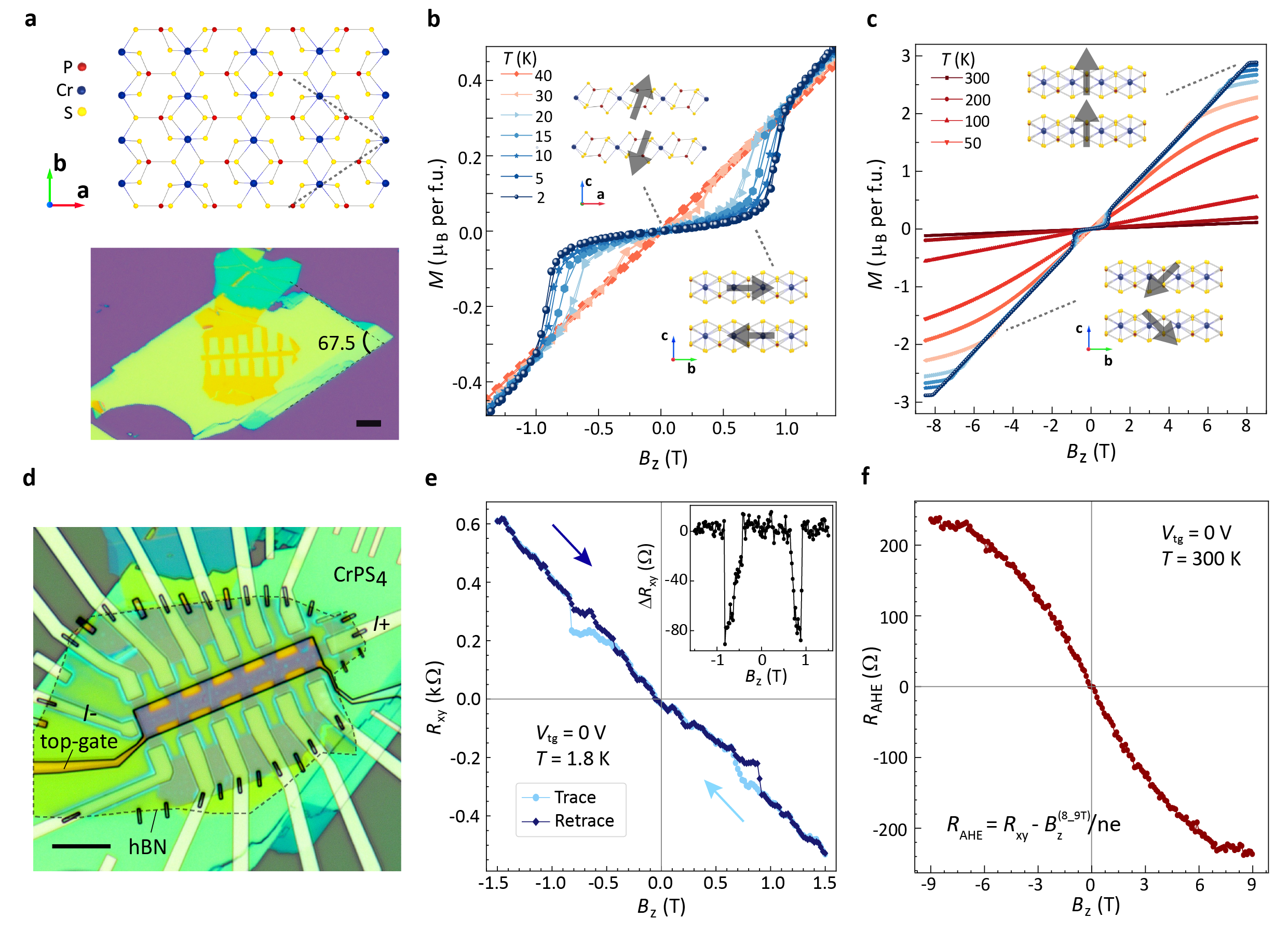
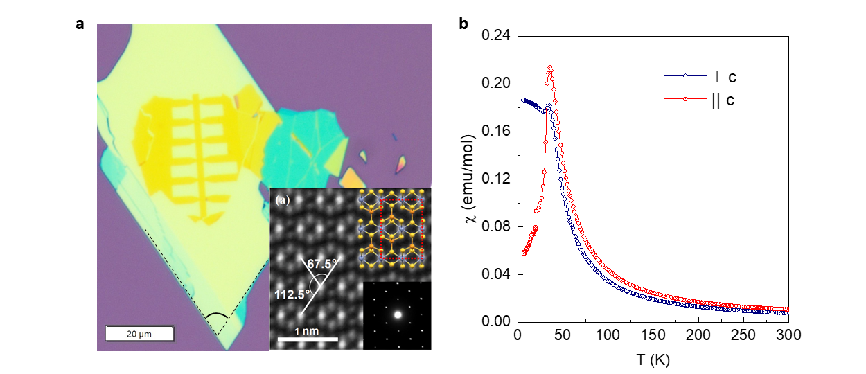
We magnetize graphene by the van der Waals proximity of the interlayer antiferromagnet, CrPS4 (CPS), which is an air-stable semiconductor with a bandgap of 1.3 eV lee2017structural and a Néel temperature of 38 K peng2020magnetic . Figure 1a (top panel) illustrates a top view of the CPS crystal structure with the dashed lines indicating the crystallographic directions along which the crystals preferentially cleave, as shown in the optical micrograph of an exfoliated flake. As a result, the CPS flakes acquire a corner angle of , the bisector of which is along the magnetic -axis lee2017structural (see also supplementary information (SI), Figure S2). The presence of this characteristic angle allows for the identification of the CPS crystallographic orientation and guides the alignment of the graphene Hall bar with one of the CPS magnetic axes (see Figure 1a, lower panel). In accordance with previous reports peng2020magnetic , CPS has an anisotropic magnetic behavior which is evaluated using a superconducting quantum interference device (SQUID) at various temperatures, shown in Figure 1b and c. The magnetic ordering of the layers in a multilayer CPS crystal at is known to be mainly out-of-plane (with spins oriented along the -axis) angled towards the -axis (as shown in the upper inset of Figure 1b). The SQUID measurements at a small (panel b) for , show a spin-flop transition when the magnetization of the layers rotate towards the -axis, whilst holding their respective anti-parallel alignment (lower inset). Increasing above the spin-flop transition field ( at ) results in canting of the magnetic moments towards the -axis with full saturation at , as shown in Figure 1c.
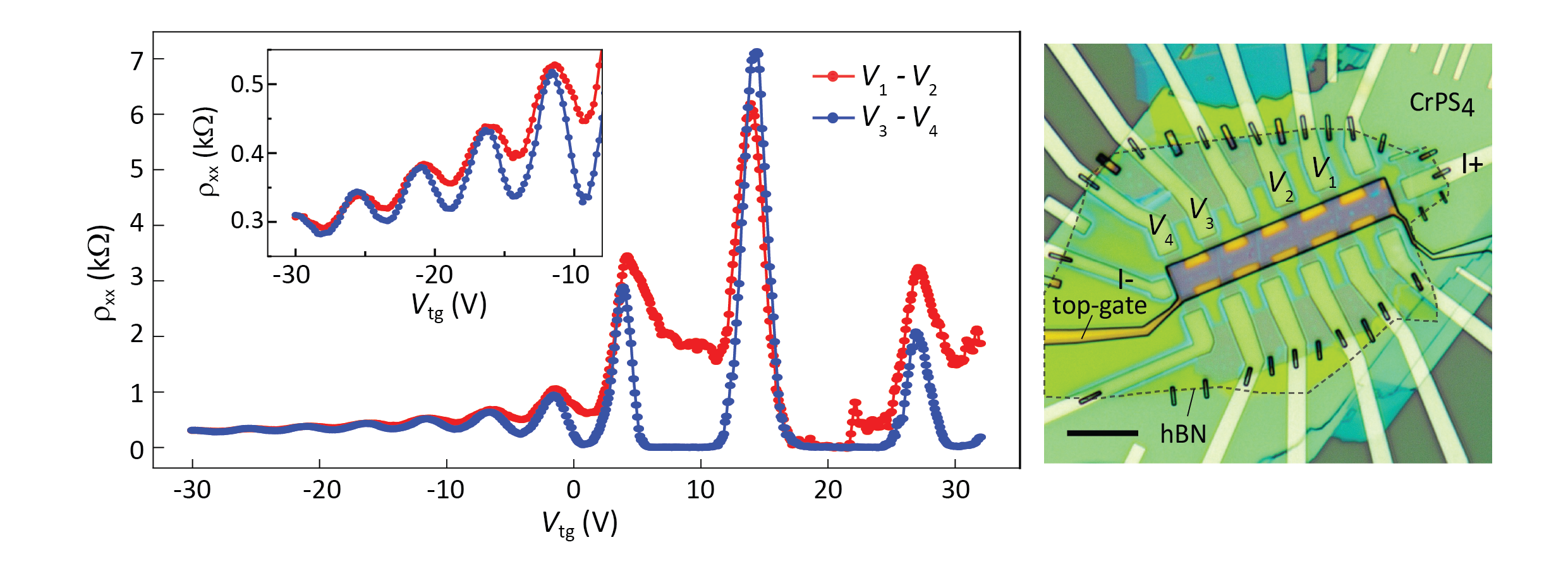
We evaluate the possibility of inducing the CPS magnetic properties in graphene by measuring the charge transport in graphene. We report on two devices (A and B), each fabricated with a monolayer graphene Hall-bar on a multilayer CPS flake, fully covered with hBN that is used as a dielectric for the top-gating (Figure 1d). We apply current along the graphene channel (with and electrodes shown in panel d) while measuring the longitudinal and transverse voltages ( and ). In Figure 1e, we show the modulation of the transverse resistance as a function of , at . Remarkably, switches at , which is the magnetic field at which the spin-flop transition occurs in CPS. This is a direct indication that the magnetic behavior of the CPS is influencing the charge transport in graphene.
The trace and retrace measurements of show no hysteresis vs. , except for close to . That is understood by considering the behavior of the magnetization of CPS outermost layer (), to which the is the most sensitive. The behavior of is ruled by its anti-ferromagnetic coupling with respect to the other CPS layers, and yet, the lack of a neighboring CPS layer on top can cause the to lag behind the magnetization dynamics of the bulk of CPS, leading to the observed hysteresis. Thus, by decreasing the , the switches back to the antiferromagnetic alignment with respect to the other CPS layers at lower fields of 0.5 T, by which in the retrace retrieves its initial value as in the trace measurement. From the difference of the in the trace and retrace measurements, which is about 80 (shown in the inset of Figure 1e), we extract a change of in the -component of the magnetic field sensed by the electrons in graphene, due to the spin-flop transition of the .
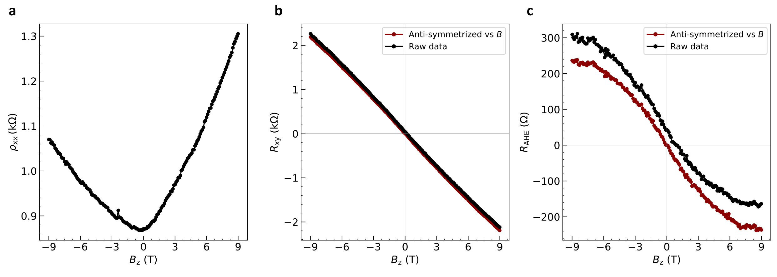
Another indication of the induced magnetism in graphene is the detection of the anomalous Hall effect which gives rise to a non-linearity of the Hall voltage. The anomalous Hall component follows the projection of the magnetization along the -axis. Thus, considering the magnetization saturation field in CPS above , we subtract the linear component related to the ordinary Hall effect from the measured . This procedure yields the anomalous Hall signal (), shown in Figure 1f, measured at and . The observation of such a sizable signal of 200 is a signature of the co-presence of large induced spin-orbit and exchange interactions nagaosa2010anomalous in the proximitized graphene up to room temperature.
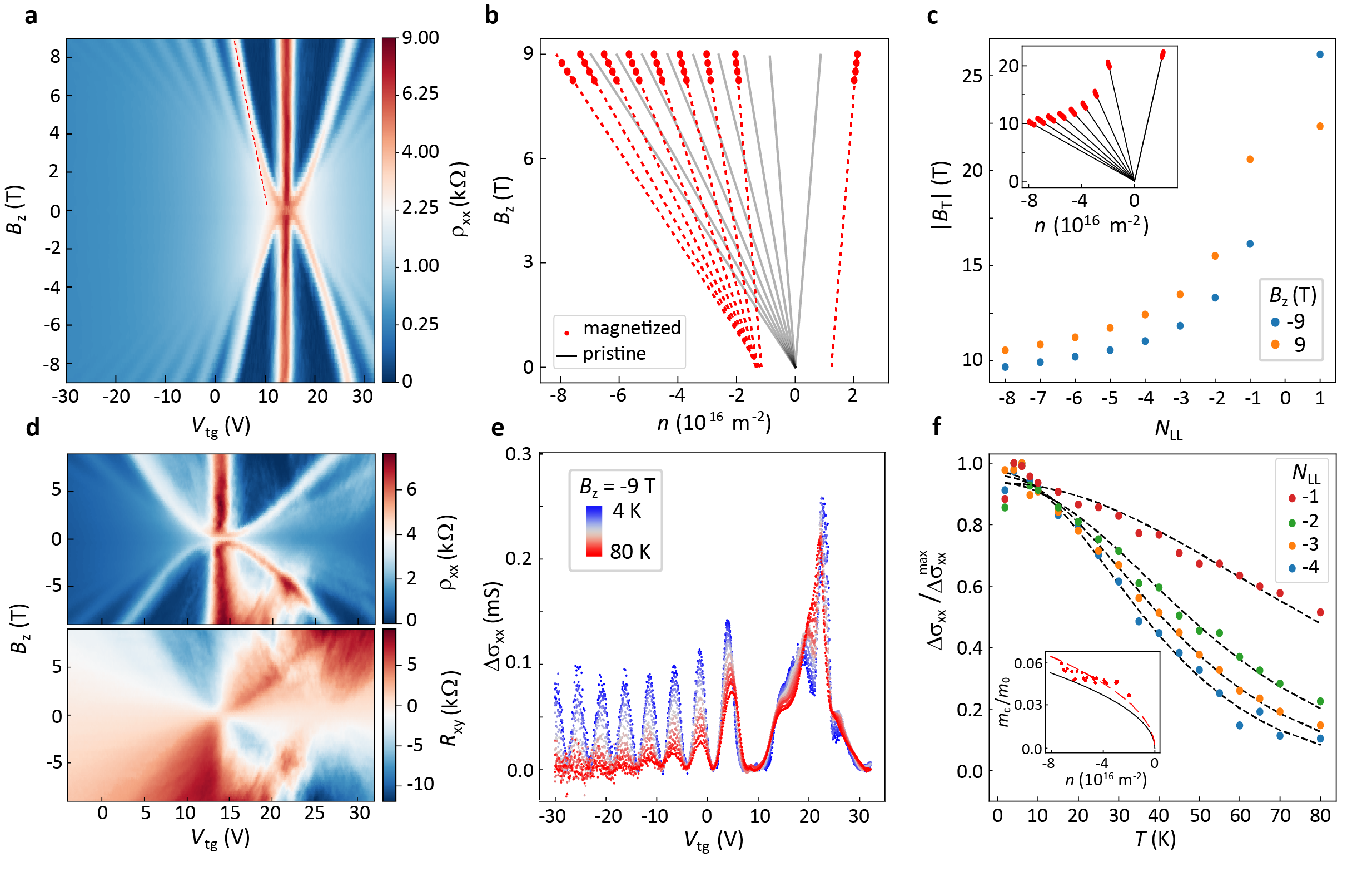
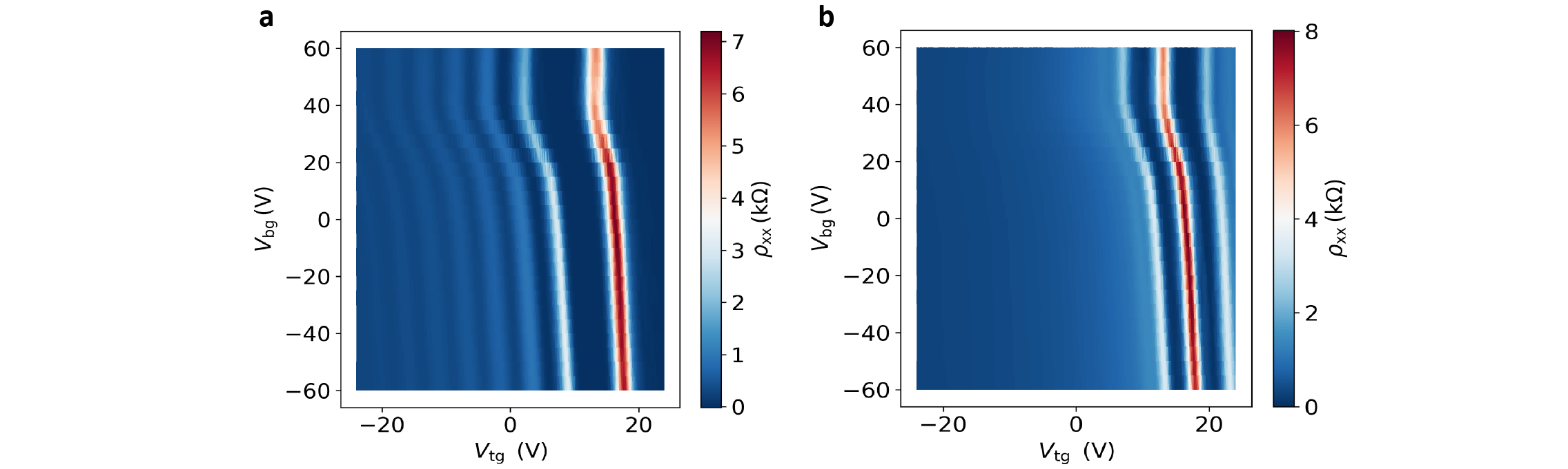
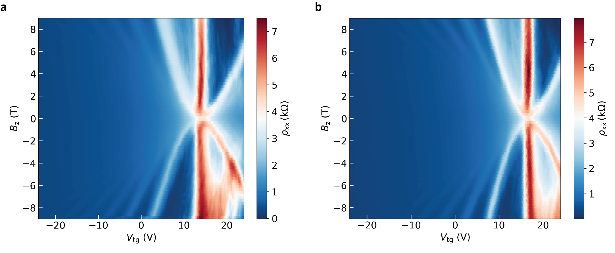
By cooling down the device, signatures of QH transport become more evident, as shown in Figure 2. Transport in the proximity-magnetized graphene is measured at for to . The modulation of the resistivity () vs. , i.e., the Shubnikov de-Haas oscillations (SdHOs), is shown in Figure 2a. The back-gate voltage () is set to to shift the Dirac point such that the electron-like Landau levels (LLs) are reachable by the top-gating. We evaluate the back-gate vs. top-gate dependence of the LLs as shown in the SI Figure S4, indicating only a shift of the LLs by electrostatic doping without any significant change in the Landau fan diagram with (also see SI Figure S5). This observation reassures the magnetic proximity effect which is in contrast to recent reports in graphene in the proximity of CrX3 tseng2022gate or CrOCl wang2022quantum , where gate-dependent interfacial charge transfer influences the transport in graphene.
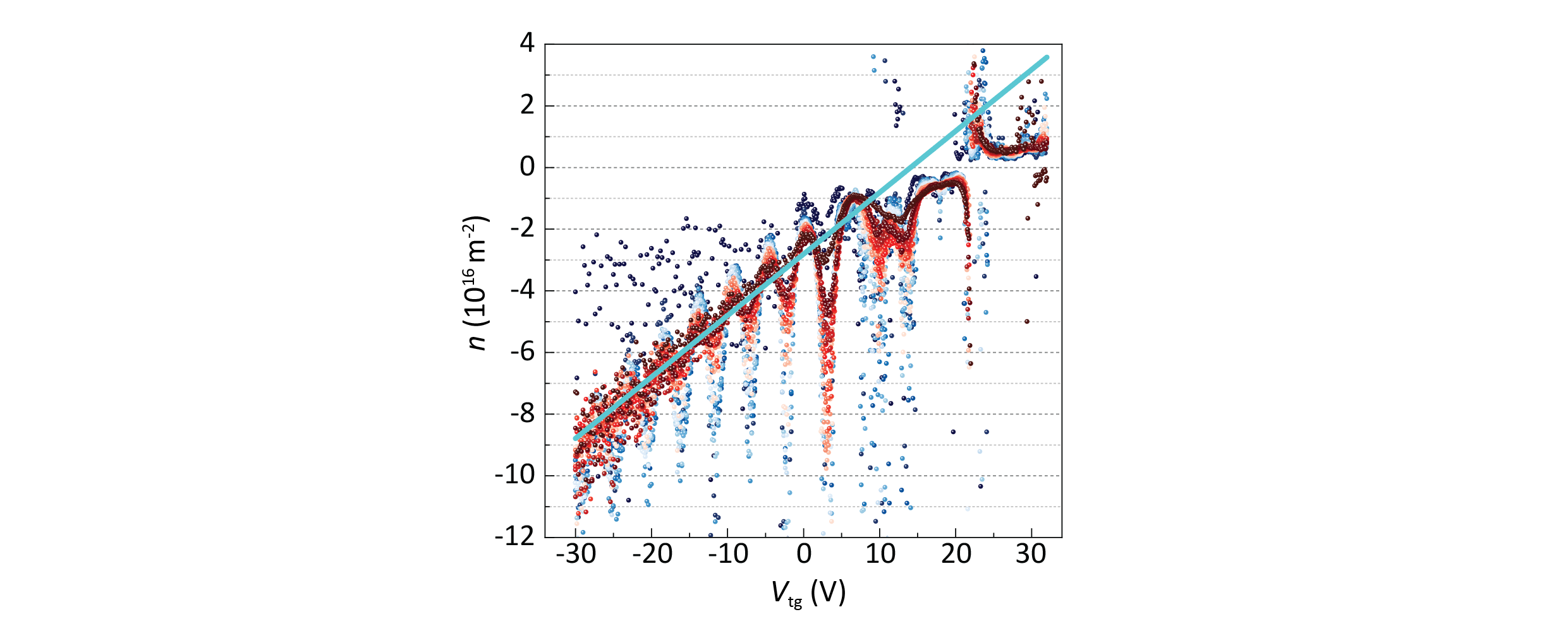
The Landau fan diagram in the magnetized graphene (Figure 2a) appears to be distinctive from that of pristine graphene, showing a large separation of the LLs with non-linearity of the first LLs close to zero energy. As indicated by the divergence from the red dashed line, the SdHO peaks deviate from the linear behavior for T. This deviation from the conventional fan diagram could be due to a non-linearity of the graphene dispersion relation close to the charge neutrality point and/or due to the non-linear behavior of vs. close to the spin-flop transition. Considering a linear dispersion relation for graphene for away from the charge neutrality point (as predicted by DFT calculations for such magnetic heterostructures zollner2022proximity ), the energy of the N LL is with being the LL number, the electron charge, the reduced Planck’s constant and the Fermi velocity novoselov2005two ; zhang2005experimental . is the total effective magnetic field sensed by the electrons which is defined as , with originating from the projection of the along the axis. This relation implies a linear dependency of carrier density vs. for each LL when is constant. For pristine graphene (), the relation results in the Landau fan shown with the gray lines in Figure 2b. Using the same equation for the magnetized graphene, we linearly fit the maxima vs. for each LL, for T when the CPS magnetization is fully out-of-plane (shown by the red dashed lines in panel b). Note, that since the graphene is encapsulated with different materials with various dielectric constants, we do not rely on the geometrical capacitance for the estimation of . Instead, we extract from the dependence of vs. for each LL which is comparable with extracted from Hall measurements that is a more reliable approach (see SI, section 7 and 8).
A direct comparison of the Landau fan diagram in pristine vs. magnetized graphene shown in Figure 2b clarifies that the carrier density at each LL is larger in the magnetized channel, and a linear extrapolation of to yields to (also see SI, section 8). This implies a larger energy separation between the LLs due to a higher effective total magnetic field sensed by the electrons, implying that . Following the vs. relation, we extract for each LL at . The result is shown in Figure 2c, with reaching 20 to for the first LLs (). This large difference between and the applied can be realized considering the induced Berry curvature in graphene xiao2010berry ; sundaram1999wave , as the dipolar magnetic field generated by the CPS is expected to be rather small. The induced Berry curvature acts as an effective magnetic field in momentum space that deforms the electron motion and modifies the LLs sundaram1999wave . The energy dependence of the extracted is also supported by the expected energy dependence of the Berry curvature induced in graphene zollner2022engineering ; bora2022magnetic .
The behavior of the transverse voltage is also addressed in a simultaneous measurement of and , shown in Figure 2d, for another pair of voltage probes. Even though additional features appear in the Landau fan (absent in panel a, measured with the first voltage pair), the position of the LLs vs. is the same (see SI, Figure S6). The expression is used to consider both longitudinal and transverse voltages in a conductivity tensor qhe_klitzing , measured at various temperatures up to (shown in Figure 2e as , obtained after standard background subtraction novoselov2005two ). From the temperature-dependence of , shown for the first few hole-like LLs in Figure 2f, we extract the effective mass of the electrons in the magnetized graphene by fitting to the standard expression , with the Boltzmann constant and the cyclotron mass novoselov2005two ; zhang2005experimental . The ratio of the cyclotron mass vs. the rest mass of the electrons (/) extracted from the SdHO at for various is shown in the inset of Figure 2f. The extracted / ratio shows a deviation from that expected for the case of pristine graphene with (indicated by the black solid line in the inset) novoselov2005two ; zhang2005experimental . From the fit to vs. , considering graphene’s linear dispersion relation, we find . The estimated and in the magnetized graphene also hint towards the modulation of the graphene band structure by the proximity of the CPS.
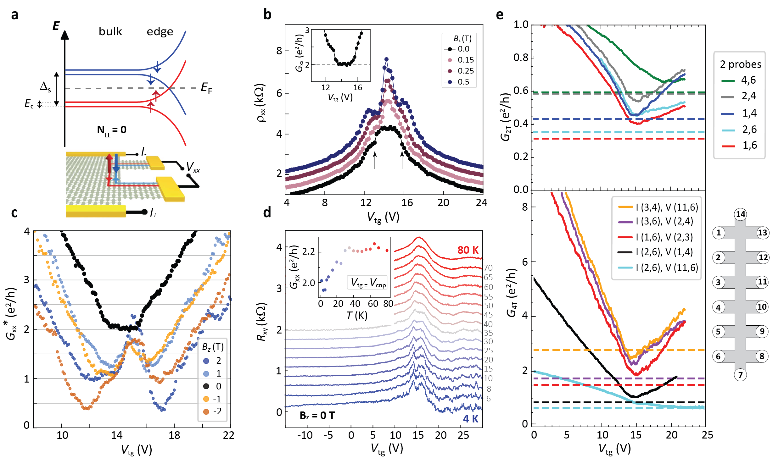
As the gate-dependence of indicates, the induced magnetism can have a stronger impact on the LLs closer to the charge neutrality point, where the spin-splitting is expected to be the largest zollner2022engineering . The zeroth LL (zLL) in graphene is formed by the wavefunctions from each valley, occupied by either electrons or holes at zero energy, leading to two spin-degenerate electron- and hole-like zLLs. By applying a perpendicular magnetic field, an energy gap () is formed between the electron- and hole-like bands, originating from Coulomb interactions due to the confinement of charges in the zLLs. Upon increasing the Zeeman spin-splitting energy (), when , a band diagram similar to that shown in Figure 3a can occur which hosts counter-propagating spin-polarized electron- and hole-like bands, so-called helical states kane2005quantum ; abanin2006spin ; kharitonov2012edge . These states are different from the chiral ones, addressed in Figure 2 at which are either electron- or hole-like and thus propagate in the same direction.
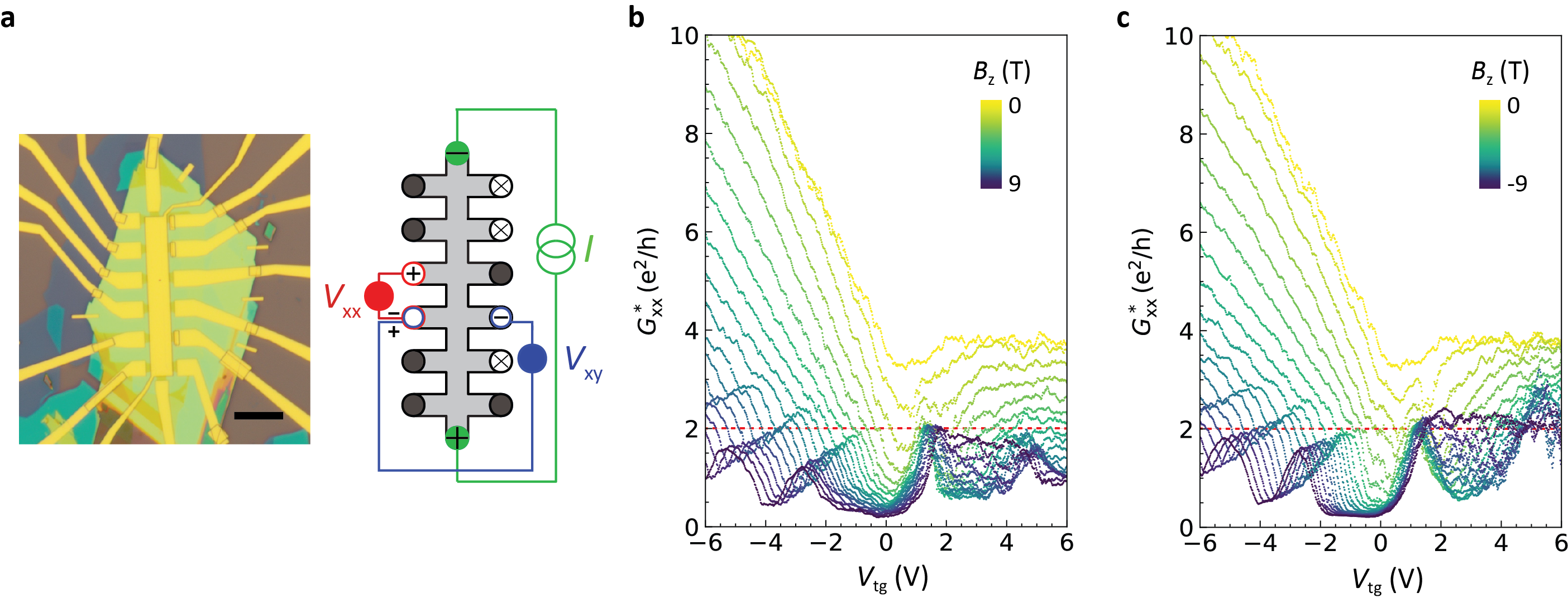
Focusing on the transport close to zero energy, shown in Figure 3b for small applied magnetic fields (), remarkably, we observe the emergence of the SdHO-associated shoulders (indicated by the arrows). This is a signature for the onset of the QAH transport in the magnetic graphene already at . Observing the SdHO implies that the condition for the Landau quantization, , with as the charge carrier mobility, is fulfilled qhe_klitzing . Since the carrier mobility in these devices is rather low (, see SI Figure S9), there must be an additional effective magnetic field of sensed by the charge carriers in the magnetic graphene to allow for the formation of the LLs. We attribute this to the finite out-of-plane component of the magnetization of the CPS at , induced in graphene which affects the orbital motion of the graphene charge carriers.
We further notice that the Dirac curve at (in Figure 3b) has a rather wide peak. When the four-terminal longitudinal measurements are evaluated in terms of conductance (), as shown in the inset of panel b and in Figure 3c (reproduced by different voltage probe pairs), it becomes evident that the broadened Dirac peak at is a plateau of conductance at . This quantized conductance at zero energy is evidence for the presence of counter-propagating spin-polarized helical states, as depicted in Figure 3a, as a result of the spin-splitting induced in graphene by the magnetic exchange interaction. In this case, the channel conductance that considers the conductivity tensor (defined as ) should go to zero as soon as transport is dominated by the chiral edge states, since they propagate only in one direction qhe_klitzing . Thus, Figure 3c shows that by increasing , goes towards zero above and below the zLL, yet it remains close to at zero energy implying that is larger than the Coulomb gap also at (see SI section 9 for device B). Note that at .
Simultaneous measurement of in Figure 3d shows that there is a finite transverse voltage at , which contains the contribution from the anomalous Hall effect as a result of the finite -component of the . Remarkably, shows a double-peak feature at zero energy that merges into a single peak at higher temperatures, due to thermal broadening. The separation of the two peaks in the in terms of energy is similar in magnitude to the width of the plateau in at zLL ( ), indicating a correlation between the longitudinal and transverse voltages, both consistent with the spin-split picture of the band diagram in Figure 3a. The temperature-dependence of at T (inset of Figure 3d) shows that the zLL conductance plateau deviates from as we raise the temperature, flattening out at around , indicating a correlation with the CPS magnetization vs. (see SI Figure S17 for the full -dependence).
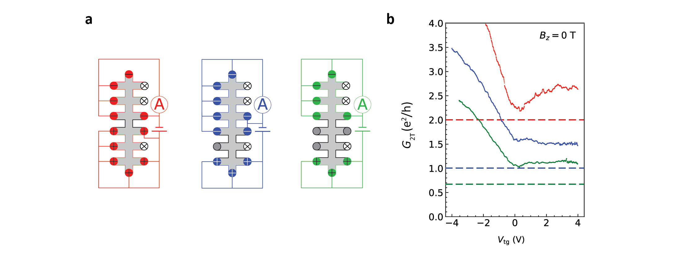
To further explore the helical nature of the edge transport at zLL at T, we investigate the effect of floating voltage probes on the transport properties of the devices. Helical charge transport occurs on both edges of the graphene channel with each edge hosting one spin-polarized state buttiker2009edge . In this case, the voltage probes present along the edges alter the conductance between the source and the drain, since the charges do not maintain their spin when entering a probe. Thus, according to the Landauer-Buttiker formalism buttiker1986 (see SI, section 12), the two-terminal conductance in the presence of two counter-propagating (helical) edge states is given by the relation:
| (1) |
where and are the number of floating probes between the source and drain, along the left and right edges of the conductor. Similarly, the four-terminal conductance is given by
| (2) |
where is the number of floating electrodes in between the source and drain along the edge which hosts the voltage probes, and is the (minimal) number of floating electrodes in between the voltage probes roth2009nonlocal . For the measurement of Figure 3c, , and , thus, the , which is exactly what is measured at at the zLL conductance plateau. Considering the equations above, we evaluate the transport in various two- and four-terminal measurement geometries, shown in Figure 3e. The expected and considering the helical edge states, in the absence of 2D bulk transport, are shown by the dashed lines that are color-coded with respect to each measurement geometry. The measured conductance in each geometry approaches the theoretical values at the Dirac point, where the bulk transport is minimized (and not fully eliminated), further supporting the contribution of helical states in the magnetized graphene at 0 T.
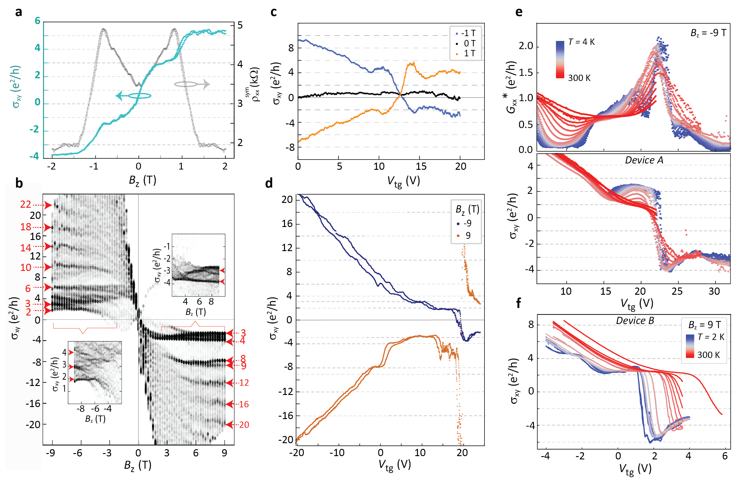
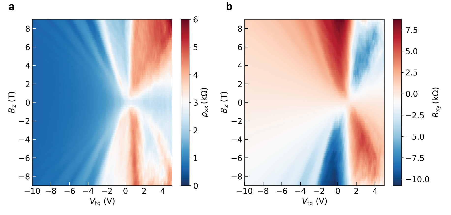
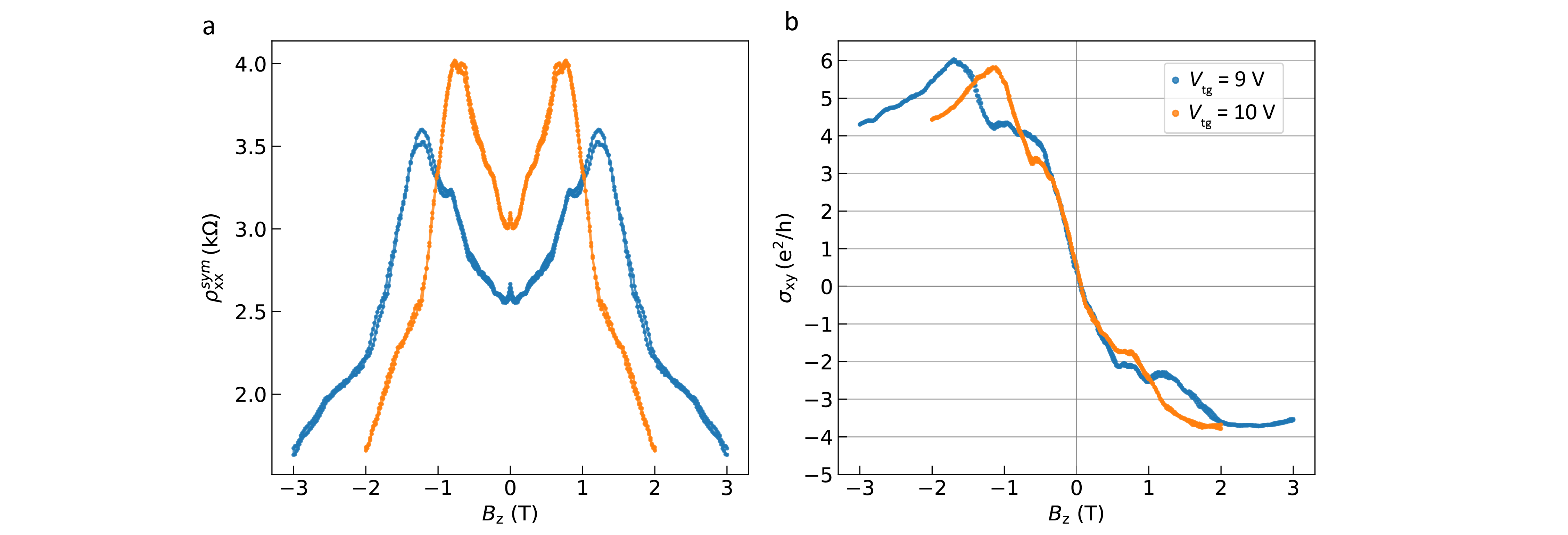
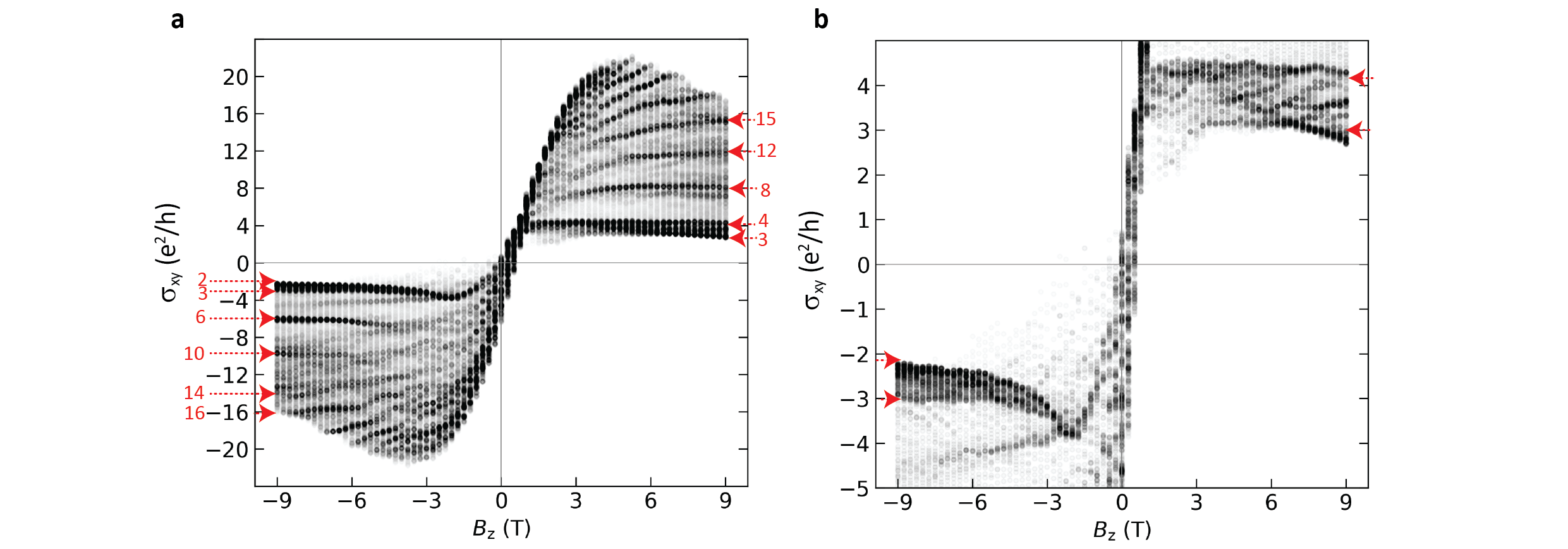
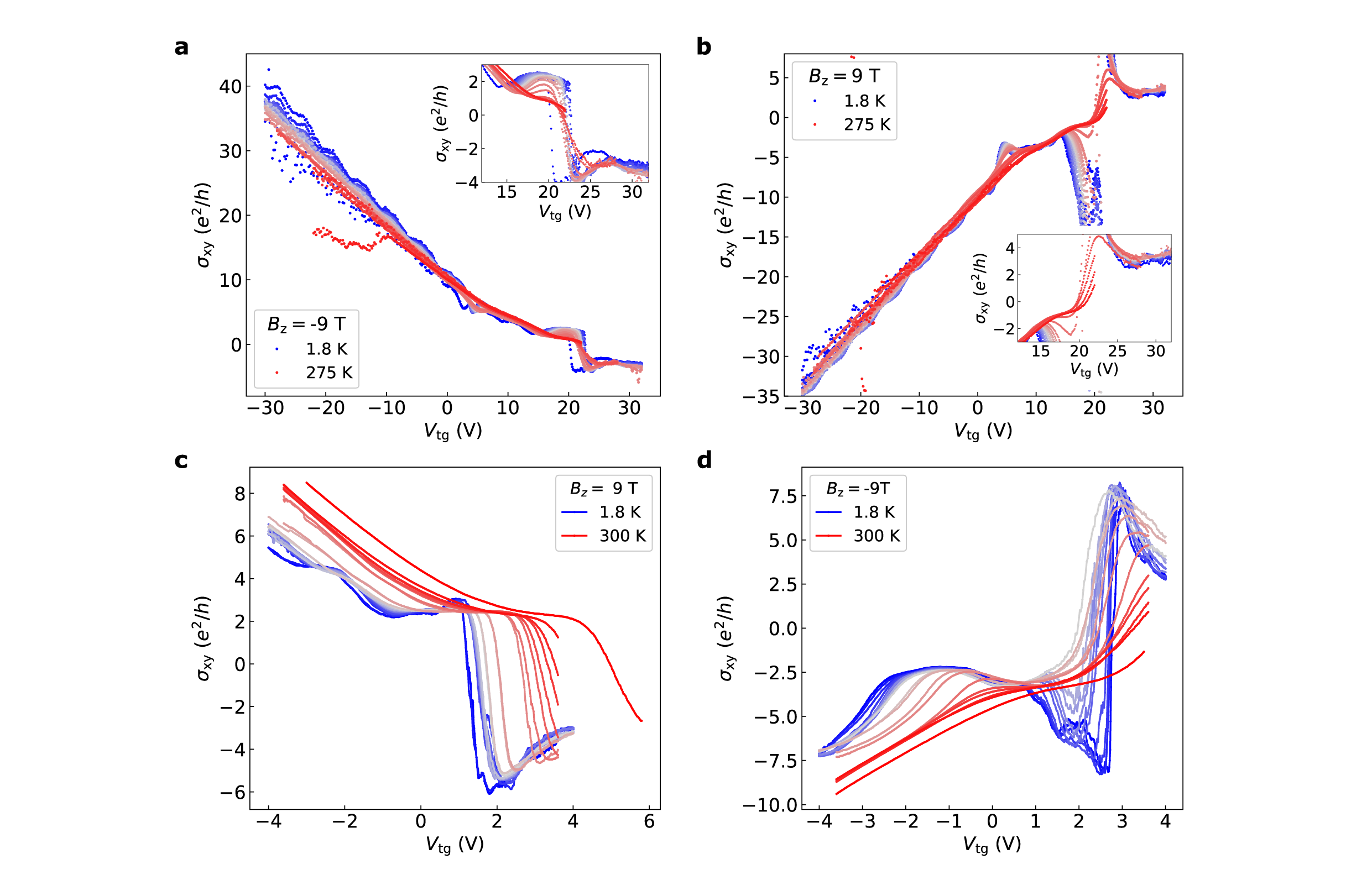
We also investigate the QAH transport () by evaluating the transverse voltage, which is a direct measure of the number of chiral edge states in the channel in the QH regime. Figure 4a shows the magnetic field dependence of the transverse conductivity () close to zero energy (). Near the SdHOs of , we observe plateau-like features in at about and at lower that reach and for . This unconventional leveling of the plateaus, with the smaller filling factors appearing at the smaller range of , can be related to the non-linear and non-monotonic behavior of CPS magnetic transition, rotating from out-of-plane to in-plane direction, at this range of the (see also Figure S15). Figure 4b further shows the dependence of on a larger range of for , where the data is shown with transparency of the markers to visualize the accumulation of data points (resulting in the darker shades) around specific values at the QH plateaus (indicated by the red arrows).
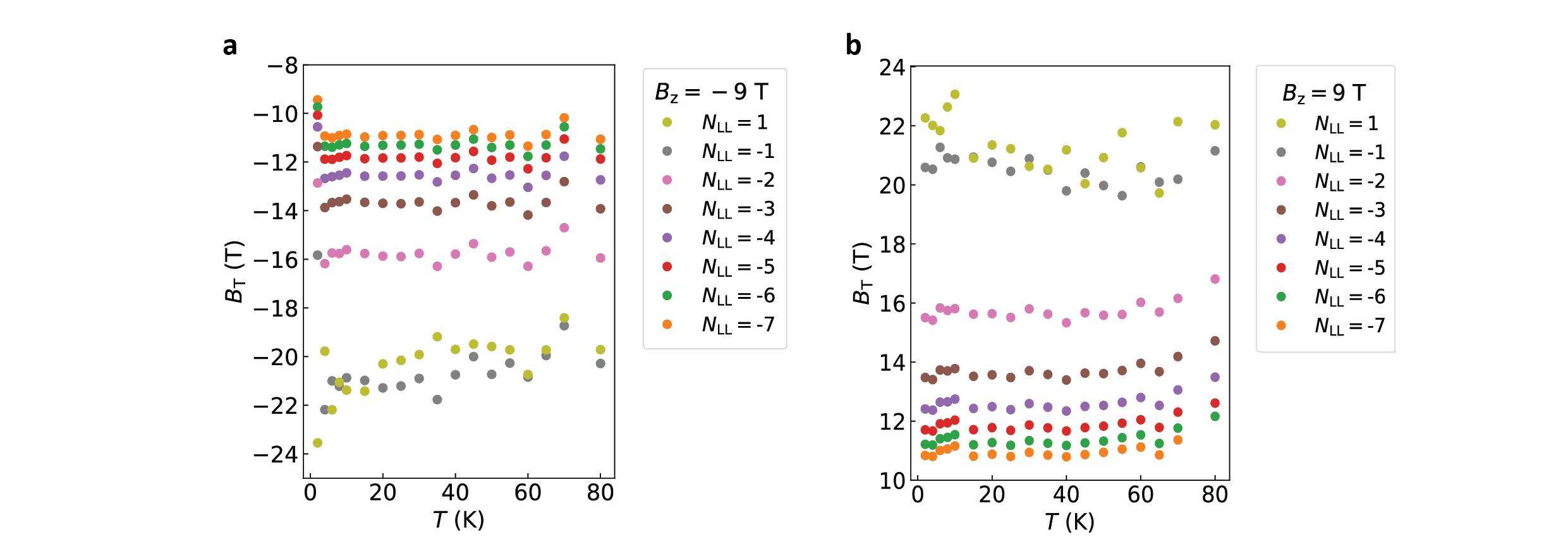
The QH plateaus appear to be asymmetric vs. and have unconventional sequences, distinct from that expected in pristine graphene ( novoselov2005two ; zhang2005experimental ). This asymmetry that is present up to high filling factors and high shows different arrangements of the LLs for , depending on the direction of the CPS magnetization. This remarkable anomaly can be explained by the -dependent interplay between spin-orbit and exchange interactions induced in graphene zollner2020scattering . In contrast to spin-orbit coupling, exchange interaction changes sign with , thus their overall contribution breaks time-reversal symmetry and alters the formation of the zLLs from the K and K’ valleys for positive vs. negative . Moreover, we observe that for the LLs with smaller filling factors, increasing creates further splitting of the levels by (shown more clearly in the insets of Figure 4b). This is an indication of spin and valley splitting of the LLs when is pulled towards the out-of-plane direction by the applied . The unconventional sequence of QH plateaus appears both at small and large magnetic fields which is presented vs. in Figure 4c and d, and is also reproduced in device B (see SI, Figure S16).
We also evaluate the QH transport up to room temperature, with a focus on the SdHO and QH plateaus close to zero energy shown in Figure 4e. In this range of , the has a maximum at right at the gate voltage at which goes to zero, pointing at the presence of the helical states up to . By increasing we observe that the conductance close to zLL decreases (see also Figure S19 and S20 for the -dependence of resistivity at in both devices). This metallic -dependence which opposes that of pristine graphene, indicates the presence of a QH metallic state at zero energy which reassures gapless LLs, consistent with the presence of the counter-propagating helical states up to large magnetic fields abanin2007dissipative . We also monitor vs. temperature which shows that the plateau-like features close to zero energy persist up to room temperature. This may be due to the enhanced Curie temperature at the graphene-CPS interface, as recently reported zhu2023interface . The -dependence of the QH transport in device B (shown in Figure 4f) also indicates that the first QH plateau at stays robust up to 300 K. The Landau plateau at , in particular, is theoretically predicted to emerge in graphene by the QAH effect qiao2010quantum ; zhang2015robust which is expected to be robust in temperature hogl2020quantum . Note that the charge carrier mobility in these devices is low, thus the very observation of QH plateaus at room temperature is due to the robustness of the QAH in graphene, enabled by the magnetic proximity of the CPS at elevated temperatures.
In conclusion, in graphene-CPS heterostructures, the induced magnetism and spin-obit coupling and their interplay allow for the emergence of quantum anomalous Hall and spin Hall effects. The out-of-plane component of the CPS magnetism induced in graphene enables the onset of the QH transport at zero external magnetic field. The induced exchange interaction causes the spin-splitting of zLLs which leads to the emergence of spin-polarized helical states in the magnetic graphene without the application of an external magnetic field. Furthermore, QAH transport results in a distinctive Landau fan diagram with large separations of the LLs, due to the presence of additional effective magnetic fields as large as 15 T which is a direct consequence of the enhanced Berry curvature in the magnetized graphene. The broken time-reversal symmetry in this system lifts spin and/or valley degeneracies and gives rise to the detection of unconventional QH plateaus. Moreover, in accordance with theoretical expectations for the QAH effect, the first quantum Hall plateaus persist up to . These observations, in particular the detection of the helical states at zero external magnetic field, in addition to the robustness of the QAH effect up to room temperature open the route for the direct applications of the magnetic graphene in 2D topological quantum spintronic devices.
Methods
CrPS4 Synthesis. CrPS4 crystals are grown following a solid-state reaction. Stoichiometric amounts of Cr (99.99 , Alfa-Aesar), P (, Sigma-Aldrich) and S (, Sigma-Aldrich) are sealed inside an evacuated quartz tube (pressure mbar, length: , internal diameter: ) and placed in a three-zone furnace. A temperature gradient of C is kept for 21 days followed by a quench into water. The obtained crystals are analyzed by powder X-ray diffraction and energy-dispersive X-ray spectroscopy. The refinement of the X-ray pattern (ICSD 25059) reveals a monoclinic C face center crystal system with C121 space group and a unit cell determined by = = 90∘ and = 91.99(1)∘ and a = 10.841(9)∘A, b = 7.247(6)∘A and c = 6.100(5)∘A. The amount of elements is Cr:, P: and S:, in good agreement with the expected ones (Cr:24.6, P: and S: ). The obtained results are in accordance with the ones previously reported in the literature peng2020magnetic .
Electrical characterization. The electrical characterization is performed using DC current source and voltages are measured using Keithleys. DC voltage source is used for the gates. The measurements are performed using a variable temperature insert at He atmosphere (in attoDry2100 system).
Acknowledgements
We would like to acknowledge Yaroslav Blanter and Anton Akhmerov for insightful discussions. This project has received funding from the European Union Horizon 2020 research and innovation program under grant agreement, No. 863098 (SPRING). J.I.A. acknowledges support from the European Union’s Horizon 2020 research and innovation programme for a Marie Sklodowska–Curie individual fellowship, No. 101027187-PCSV. E.C and S.M.-V. acknowledge support from the European Union (ERC AdG Mol-2D 788222, FET OPEN SINFONIA 964396), and the Spanish MCIN (2D-HETEROS PID2020-117152RB-100 and Excellence Unit “María de Maeztu” CEX2019-000919-M). K.W. and T.T. acknowledge support from the JSPS KAKENHI (Grant Numbers 21H05233 and 23H02052) and World Premier International Research Center Initiative (WPI), MEXT, Japan.
Author Contributions
T.S.G. and H.S.J.v.d.Z. conceived and designed the experiments. T.S.G. performed device fabrication and measurements with the help of D.P. T.S.G. and D.P. analyzed the data with the help of J.I-A.. T.B. and J.I-A. assisted with measurements. S.M-V. and E.C. synthesized the CPS crystals and performed the CPS magnetometry measurements. K.W. and T.T. synthesized the hBN crystals. T.S.G. wrote the manuscript with the help of D.P. and contributions from all co-authors.
Supplementary Information
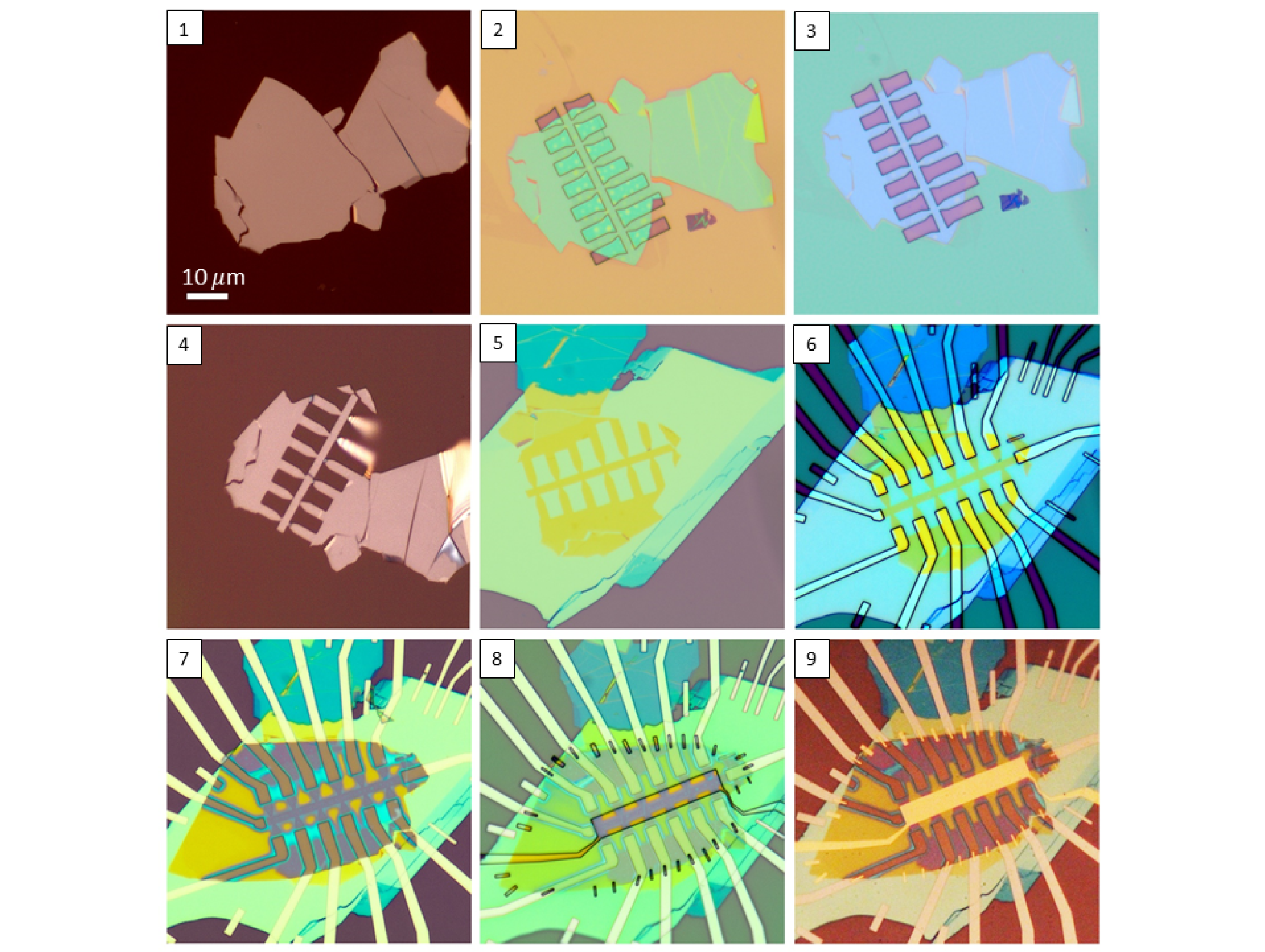
1. Device Fabrication
Figure S1 shows the steps for the fabrication of device A. Details of the fabrication steps are stated in the caption. Device B is also fabricated using the same procedure.
2. CPS magnetization anisotropy
3. -dependence of the longitudinal and transverse resistivity at room temperature
4. Evaluation of interfacial charge transfer by top-gate vs. back-gate sweeps
In previous studies on graphene in the proximity of 2D magnetic materials, gate-dependent interfacial charge transfer from the 2D magnet to the graphene has been reported tseng2022gate ; wang2022quantum . That has given rise to the observation of unconventional Landau fan diagrams that flatten off vs. gate due to the suppression of the gate action by the charge transfer. To investigate the possible gate-dependent interfacial charge transfer in our graphene-CrPS4 heterostructure, we conducted similar measurements where both top- and back-gates were swept. Figure S4 show the versus and measured at different magnetic fields in device A. We observe that increasing the shifts the position of the charge neutrality point, while the Landau gaps stay constant. In Figure S5, we further show the Landau fans measured at and , indicating no significant change in the fan diagrams. As the back gate voltage is only shifting the position of the charge neutrality point, and the Landau gaps remain constant for the full and range, we can conclude that the charge transfer from the 2D magnet is minimal in our devices and does not affect the QH transport in the graphene channel.
Moreover, a recent report on transport in CPS using graphite contacts wu2023gate shows the onset of current in CPS at gate electric field above at with the resistivity of the bulk CPS to be at least 3-4 orders of magnitude larger than that of graphene. Additionally, in contrast to the large temperature-dependent charge transport reported in CPS wu2023gate , our QH measurements at various temperatures (shown in Figure 2e of the main manuscript) do not show any signature correlating with the CPS thermal activation. Thus, we confirm the suppression of the gate-activated interfacial charge transfer between graphene and CPS in the heterostructure. That is of high importance as it assures that the modulation of the LLs is due to the magnetic proximity effect, rather than to the charge-related effects. Furthermore, we note that in our devices there have been several contacts that have been used to only address the transport in the CPS. Our 2T measurements in CPS up to RT do not show any current flow in the CPS above the noise level (pA). This confirms that there is no parallel transport in the CPS layer.
5. SdHOs detected at different regions of device A
6. Landau fan diagram in device B
7. Carrier density and mobility
Encapsulation of the graphene between hBN and the 2D magnet can change the environmental dielectric constant which results in an effective capacitance that is different from the geometrical one. Thus, in a more reliable approach, we estimate the carrier density from the Hall voltage, measured vs. at various gate voltages and temperatures (in section 8 we discuss another approach for the extraction of ). At each top-gate voltage, the Hall component is separated from the anomalous Hall component and is related to the carrier density according to
| (3) |
where . We extract from the -dependence of at each , by taking the slope of vs. for . In Figure S8 we show the gate-dependence of the extracted from the Hall effect for device A. Using the linear fit between and , we obtain an effective dielectric constant of around 2.7, which is less than the dielectric constant of hBN ( laturia2018dielectric ).
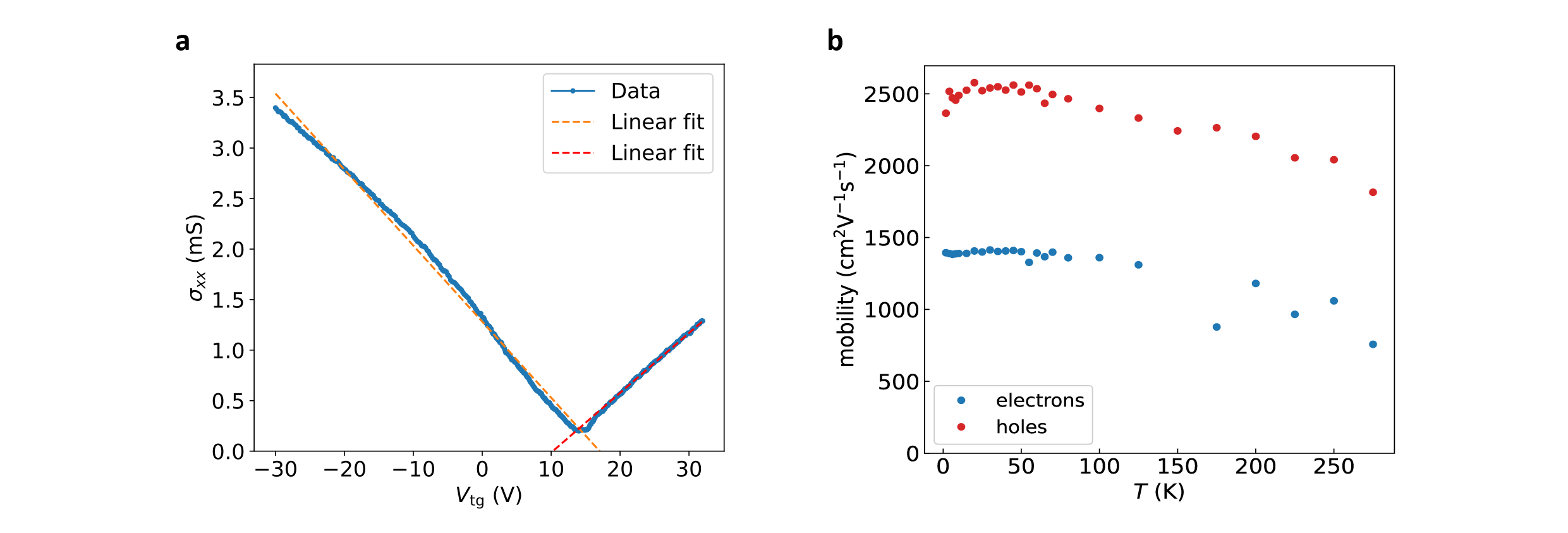
To obtain the mobility of charge carriers in the graphene channel, we refer to the relation . The is plotted versus , shown in Figure S9a, for device A. By considering the versus relation, described earlier, and by the linear fits to the vs. , we obtain and for device A, and and for device B at .
We further extract the mobility at various temperatures, shown in Figure S9b. In previous reports mobility_Vs_T1 ; mobility_vs_T2 , pristine graphene encapsulated with hBN shows a slight decrease in mobility upon increasing the temperature, whereas, in graphene on SiO2, the mobility decreases more rapidly due to higher electron-phonon interaction. In our samples, the mobility stays constant up to , especially for the electrons, and then decreases more rapidly at higher temperatures. Apart from the contribution from electron-phonon scattering, the temperature dependence in our devices could also be affected by the enhancement of the thermal fluctuations of the magnetic moments in CPS at temperatures above the Néel temperature. In device B, we extract the mobility for holes to be and at 1.8 K and RT, respectively.
8. Estimation of total magnetic field from Landau fan diagrams
The energy of the Landau levels, , in pristine graphene is given by the relation:
where and is the Landau level index. Considering the relation above and the dispersion relation in graphene, we obtain:
| (4) |
where is the flux quantum and is the carrier density. The position of the LLs depends on the total magnetic field applied to the graphene, which in our magnetized system is the sum of the external magnetic field and the field originating from the CPS magnetization induced by the CPS, i.e. . To extract the from the Landau fan diagram, we investigate the measurements at . In this range of , the CPS magnetization is supposed to be fully saturated out-of-plane, meaning that the change in the position of the SdHOs is only determined by the change in . With this consideration, the equation linearly relates and in the range .
As mentioned in section 7, one reliable approach to extract is by considering the Hall resistance at . However, we can also extract , from the vs. dependence of the SdHO peaks for each LL, considering the following relation:
| (5) |
assuming a linear relation between and , we make a linear fit to the (extracted for each LL) vs. , shown by the red line in Figure S10a. The extracted by this approach is comparable with that extracted from Hall measurements (shown by the blue line). In Figure S10b we compare the obtained using the extracted by both approaches. For the extraction of the in the main manuscript, we stick to the second approach described here for obtaining , which gives a lower bound for the estimation of the . Note that if is extracted from the geometrical capacitance, it would give rise to much larger values.
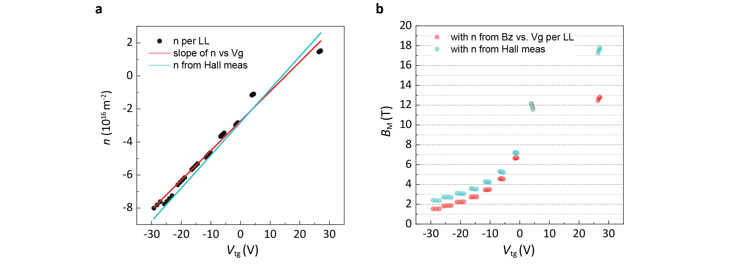
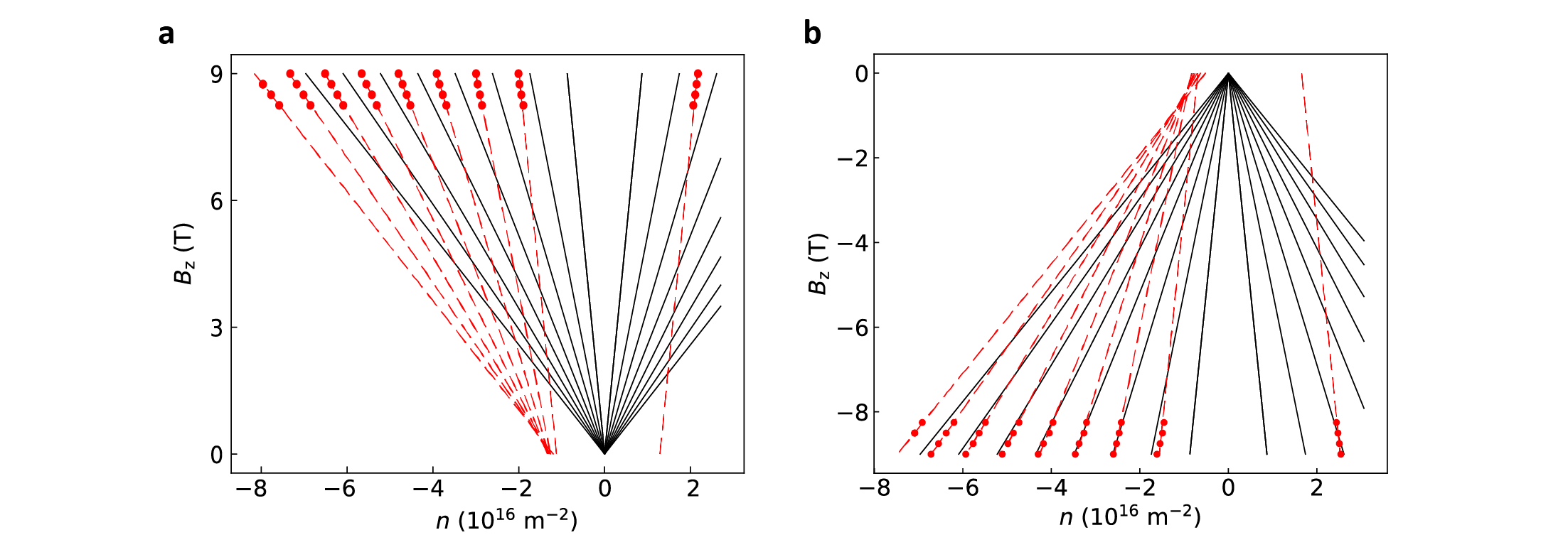
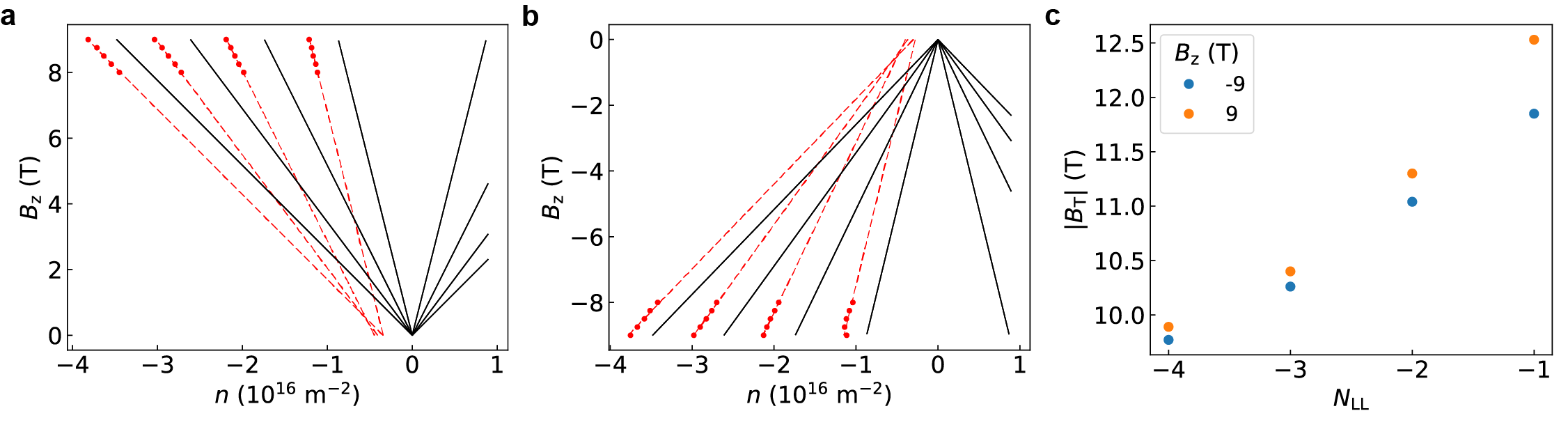
Figures S11 and S12 show linear fits for vs. for each LL, given by the red dashed lines for and , determined for device A and B. Direct comparison of the black solid with the red dashed lines clarifies that the in the magnetized graphene. With being the only unknown in Equation 5, we can obtain the total field for each LL which is shown in Figure 2c of the main manuscript (for device A) and in Figure S12c (for device B). Note that all the measurements compared for devices A and B are performed at the same .
9. Helical states in device B
We also evaluate the presence of helical states in device B, by focusing on the gate dependence of the conductance close to the charge neutrality point. We start with four-terminal geometry as shown in the schematics of Figure S13a. The gate-dependence of the four-terminal longitudinal conductance () for positive and negative ranges of is shown in panel b and c. We realize that, unlike the observations in device A, the conductance close to the charge neutrality point, measured in this geometry at , does not reach the theoretical value of 2e2/h expected for the helical states. This could be due to a larger contribution or dominance of the bulk transport as compared with edge transport at in this device, because of a smaller at (see Figure S12). However, by applying the as small as the channel is brought more in the QH regime where the transport is dominated by the edge states close to the charge neutrality point. With that, we observe that the reaches 2 at the Dirac point and stays at that value for the whole range of . Thus, this observation also reassures the emergence of the helical states in the graphene/CPS heterostructure.
We further conducted two-terminal measurements in device B, applying AC voltage and measuring current, shown in the schematics of Figure S14a. The 2T conductance () measured at for different distances shown in the device schematics, indicates that the at the charge neutrality point gets close to the theoretically expected values for the helical states (shown by the dashed lines). Yet, the is not fully matching with the expected values, as also observed in device A (Figure 3e) which once again indicates the finite contribution of bulk transport at . It is worth noting that the distance between the source and the drain in these configurations is relatively long and the device has shown to be inhomogeneously doped along the channel. With that and considering the low mobility of the charge carriers, coherent spin-polarized edge transport over such long distances is unlikely to occur, which can explain the discrepancy between the theory and the experiment.
10. Magnetic field dependence
Here we show the magnetic field dependence of and in device A measured at two other gate-voltages close to the charge neutrality point, 9 and , to be compared with the one shown in Figure 4a of the main manuscript for . We consistently observe small plateau-like features at small range that can be correlated with the low-field magnetization behavior of CPS that can affect the filling factor.
In Figure S16 we show the transverse conductivity in device B, to be compared with that of device A (shown in Figure 4b of the main manuscript). We observe the QH plateaus in device B also appear with an unconventional sequence, similar to that of device A, together with a large asymmetry with respect to .
11. Temperature dependence
In this section, first, we provide further information on the transport in devices A and B at and then we elaborate on the measurements at . In Figure S17 we show the dependence of the channel conductance at the zeroth LL (Dirac point) in device A.

We further investigate the temperature dependence of in device B, which is shown in Figure S18a measured at for 1.8 to . The gate-dependence of , shown in Figure S18b also exhibits a double-peak feature at the Dirac point (), similar to the same measurement conducted in device A (shown in Figure 3d of the main manuscript). Note that the second bump in at is associated with the inhomogeneity in the channel.
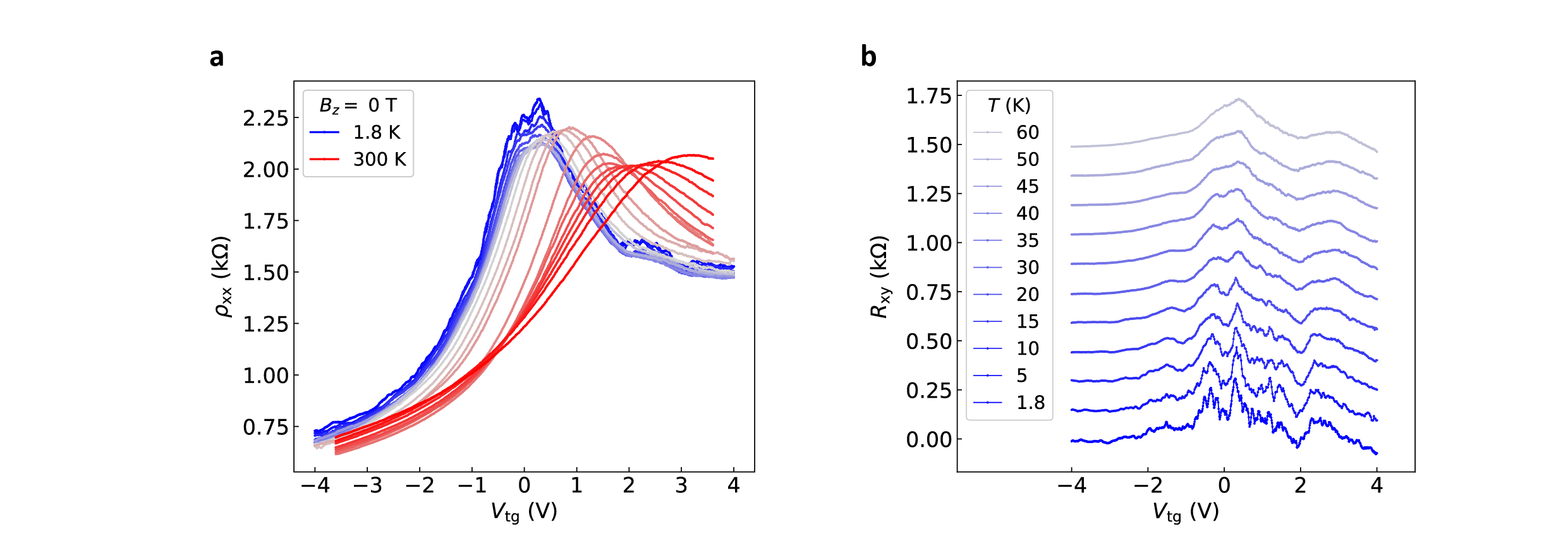
Figure S19 and Figure S20 show the temperature dependence of versus for device A and B. We observe that the charge neutrality point shifts to higher gate voltages with temperature, as the doping of the graphene channel slightly changes. The Landau levels become less pronounced as the temperature increases due to the thermal broadening. In both devices, at the Dirac point (), increases by increasing temperature. This metallic behavior is an indication of the presence of a gap-less zeroth Landau level which supports the band alignment shown in Figure 3a of the main manuscript, and so the presence of helical states. Moreover, the oscillation in related to the first Landau level, in both devices, persists up to close to room temperature. While the SdHOs merge into the background resistance (from the bulk of the graphene channel), the one related to remains as a kink or shoulder near the Dirac point (e.g. shown in Figure S19f) which indicates the robustness of the first LL against temperature. This is further evaluated through the dependence of .
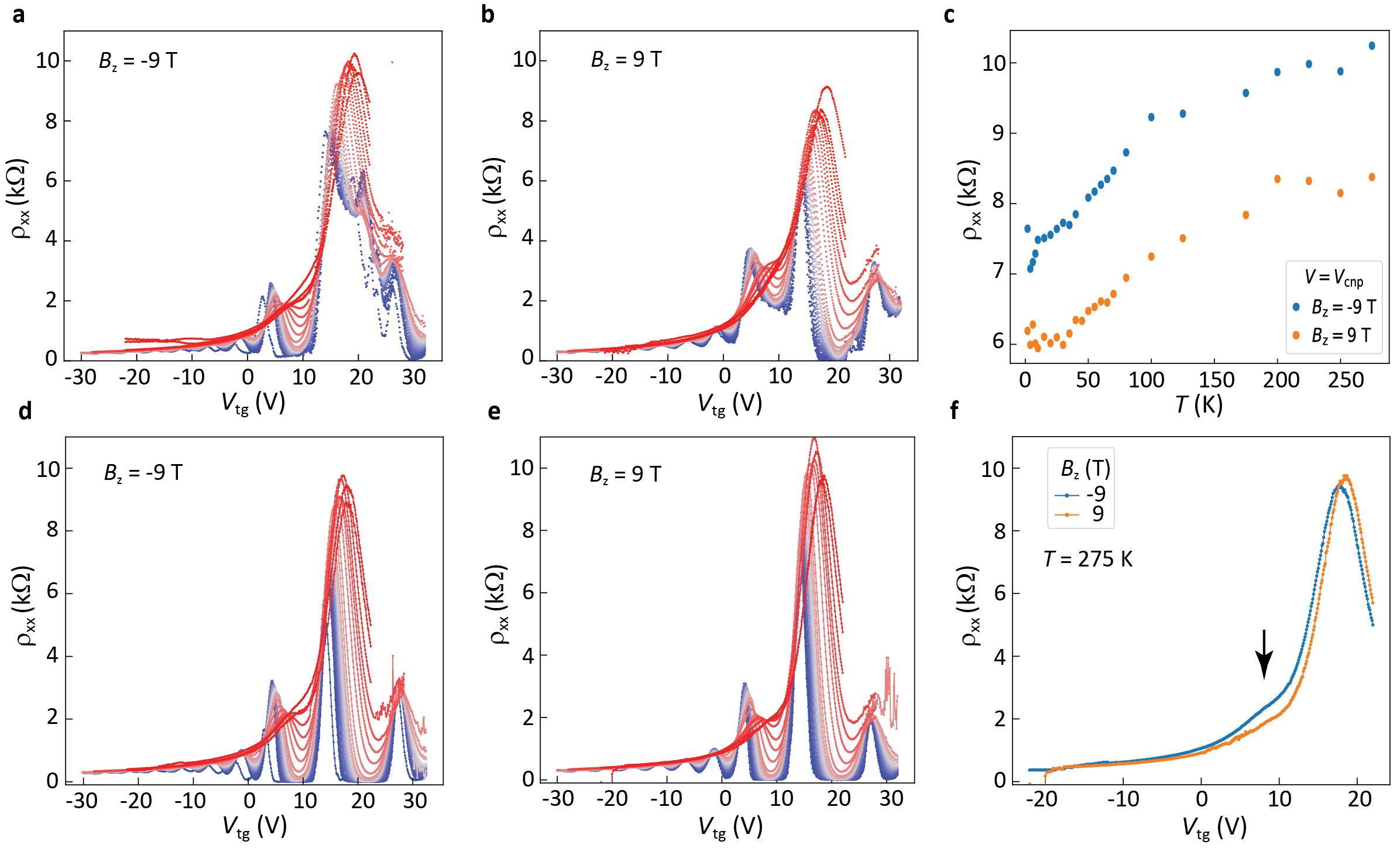
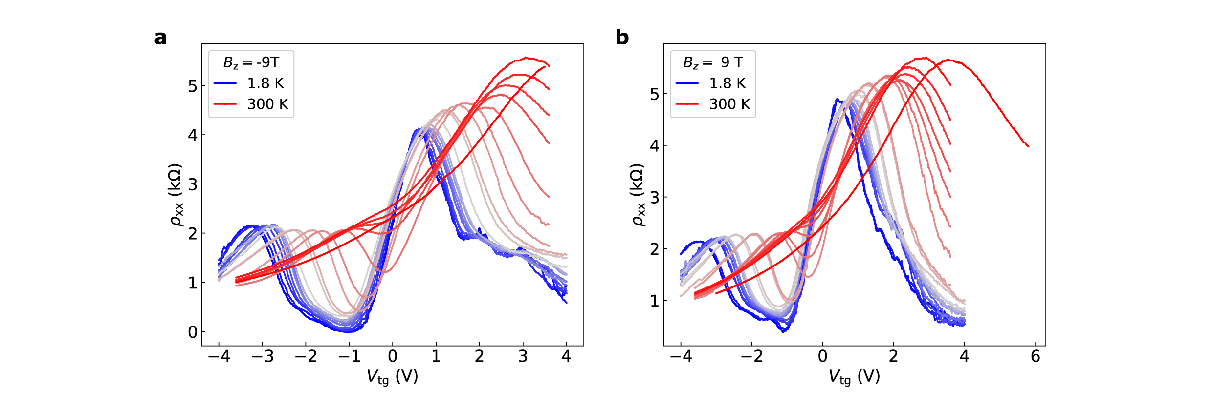
Figure S21 shows the temperature dependence of versus for device A (a, b) and device B (c, d) at . For both devices, the plateaus corresponding to higher Landau level indexes become less pronounced as the temperature increases. Both devices show a sequence of and across the Dirac point (Figure S21a and c). As the temperature increases, the plateau at remains for device B up to (panel c), whereas for device A (inset of panel a), the QH plateau gradually changes to , yet the plateau at persists up to high temperatures. Note that the sign convention of the voltage probes in device A and B has been opposite to each other during the measurements, thus the results of device A at -9 T should be compared with that of device B at +9 T.
According to theoretical predictions, if the quantum anomalous Hall effect is present in graphene, it is expected to be robust against disorders and thus should persist up to elevated temperatures hogl2020quantum . Thus, the persistence of the QH-related features in the device up to room temperature in such devices which have rather poor mobility is only reassuring that the transport is ruled by the quantum anomalous Hall effect, made possible by the CPS paramagnetic state at RT. Figure S22 shows the temperature dependence of extracted at (as explained in section 8), obtained for device A. The dependence shows that the is changing by about or less than 5 percent for the shown range. This can be related to the fact that the ferromagnetic ordering in CPS persists up to elevated temperatures when it is interfaced with graphene zhu2023interface .
12. Landauer-Büttiker formalism
To model the role of the edge channels on the measured signals, we have used the Landauer-Büttiker equation buttiker1986 :
| (6) |
where is the current in terminal , the transmission probability from electrode to electrode , and the voltage at electrode . To account for all the electrodes in device A, for instance, we have modeled for a device geometry with 14 electrodes that are connected in a closed loop where contact 14 is between 13 and 1 (as shown in the schematics of Figure 3e of the main manuscript). In this case, the component of Equation 6 is linearly dependent on the other components ( 1 to 13). To determine to , we have written Equation 6 for the terminals 1 to 13 and replaced the component with the condition , where is the potential at the grounded contact. The resulting system is shown here:
which we write as , where describes the input currents, the output voltages, and is the matrix obtained from the above considerations. and are the number of edge modes propagating from electrode to electrode and to , respectively. The last row of , and or , . Finally, we calculate using , where is the inverse of , and obtain the potentials in the 14 terminals as a function of and . Using the Landauer-Büttiker formalism, we acquire the equations 1 and 2 in the main text for two- and four-terminal conductance at the Dirac point where and , to consider for a co-presence of an electron-like and hole-like band.
References
- (1) Neto, A. C., Guinea, F., Peres, N. M., Novoselov, K. S. & Geim, A. K. The electronic properties of graphene. Reviews of Modern Physics 81, 109 (2009).
- (2) Han, W., Kawakami, R. K., Gmitra, M. & Fabian, J. Graphene spintronics. Nature Nanotechnology 9, 794–807 (2014).
- (3) Sierra, J. F., Fabian, J., Kawakami, R. K., Roche, S. & Valenzuela, S. O. Van der Waals heterostructures for spintronics and opto-spintronics. Nature Nanotechnology 16, 856–868 (2021).
- (4) Wei, P. et al. Strong interfacial exchange field in the graphene/EuS heterostructure. Nature Materials 15, 711–716 (2016).
- (5) Safeer, C. et al. Room-temperature spin Hall effect in graphene/MoS2 van der Waals heterostructures. Nano Letters 19, 1074–1082 (2019).
- (6) Mendes, J. et al. Spin-current to charge-current conversion and magnetoresistance in a hybrid structure of graphene and yttrium iron garnet. Physical Review Letters 115, 226601 (2015).
- (7) Ghiasi, T. S., Kaverzin, A. A., Blah, P. J. & Van Wees, B. J. Charge-to-spin conversion by the rashba-edelstein effect in two-dimensional van der Waals heterostructures up to room temperature. Nano Letters 19, 5959–5966 (2019).
- (8) Benítez, L. A. et al. Tunable room-temperature spin galvanic and spin Hall effects in van der Waals heterostructures. Nature Materials 19, 170–175 (2020).
- (9) Wang, Z., Tang, C., Sachs, R., Barlas, Y. & Shi, J. Proximity-induced ferromagnetism in graphene revealed by the anomalous Hall effect. Physical Review Letters 114, 016603 (2015).
- (10) Ghiasi, T. S. et al. Electrical and thermal generation of spin currents by magnetic bilayer graphene. Nature Nanotechnology 16, 788–794 (2021).
- (11) Geim, A. K. & Grigorieva, I. V. Van der Waals heterostructures. Nature 499, 419–425 (2013).
- (12) Yang, H.-X. et al. Proximity effects induced in graphene by magnetic insulators: first-principles calculations on spin filtering and exchange-splitting gaps. Physical Review Letters 110, 046603 (2013).
- (13) Dyrdał, A. & Barnaś, J. Anomalous, spin, and valley Hall effects in graphene deposited on ferromagnetic substrates. 2D Materials 4, 034003 (2017).
- (14) Diehl, R. & Carpentier, C.-D. The crystal structure of chromium thiophosphate, CrPS4. Acta Crystallographica Section B: Structural Crystallography and Crystal Chemistry 33, 1399–1404 (1977).
- (15) Young, A. et al. Tunable symmetry breaking and helical edge transport in a graphene quantum spin Hall state. Nature 505, 528–532 (2014).
- (16) Veyrat, L. et al. Helical quantum Hall phase in graphene on SrTiO3. Science 367, 781–786 (2020).
- (17) Qiao, Z. et al. Quantum anomalous Hall effect in graphene from rashba and exchange effects. Physical Review B 82, 161414 (2010).
- (18) Tse, W.-K., Qiao, Z., Yao, Y., MacDonald, A. & Niu, Q. Quantum anomalous Hall effect in single-layer and bilayer graphene. Physical Review B 83, 155447 (2011).
- (19) Qiao, Z., Jiang, H., Li, X., Yao, Y. & Niu, Q. Microscopic theory of quantum anomalous Hall effect in graphene. Physical Review B 85, 115439 (2012).
- (20) Qiao, Z. et al. Quantum anomalous Hall effect in graphene proximity coupled to an antiferromagnetic insulator. Physical Review Letters 112, 116404 (2014).
- (21) Zhang, J., Zhao, B., Yao, Y. & Yang, Z. Quantum anomalous Hall effect in graphene-based heterostructure. Scientific Reports 5, 10629 (2015).
- (22) Zhang, J., Zhao, B., Yao, Y. & Yang, Z. Robust quantum anomalous Hall effect in graphene-based van der Waals heterostructures. Physical Review B 92, 165418 (2015).
- (23) Zanolli, Z. et al. Hybrid quantum anomalous Hall effect at graphene-oxide interfaces. Physical Review B 98, 155404 (2018).
- (24) Högl, P. et al. Quantum anomalous Hall effects in graphene from proximity-induced uniform and staggered spin-orbit and exchange coupling. Physical Review Letters 124, 136403 (2020).
- (25) Wang, X.-L. Dirac spin-gapless semiconductors: promising platforms for massless and dissipationless spintronics and new (quantum) anomalous spin Hall effects. National Science Review 4, 252–257 (2017).
- (26) Song, H.-D. et al. Electrical control of magnetic proximity effect in a graphene/multiferroic heterostructure. Applied Physics Letters 113 (2018).
- (27) Song, H.-D. et al. Asymmetric modulation on exchange field in a graphene/BiFeO3 heterostructure by external magnetic field. Nano Letters 18, 2435–2441 (2018).
- (28) Wu, Y. et al. Large exchange splitting in monolayer graphene magnetized by an antiferromagnet. Nature Electronics 3, 604–611 (2020).
- (29) Wu, Y. et al. Magnetic exchange field modulation of quantum Hall ferromagnetism in 2d van der Waals CrCl3/graphene heterostructures. ACS Applied Materials and Interfaces 13, 10656–10663 (2021).
- (30) Chau, T. K., Hong, S. J., Kang, H. & Suh, D. Two-dimensional ferromagnetism detected by proximity-coupled quantum Hall effect of graphene. npj Quantum Materials 7, 1–7 (2022).
- (31) Wang, Y. et al. Quantum Hall phase in graphene engineered by interfacial charge coupling. Nature Nanotechnology 1–8 (2022).
- (32) Tseng, C.-C. et al. Gate-tunable proximity effects in graphene on layered magnetic insulators. Nano Letters (2022).
- (33) Lee, J. et al. Structural and optical properties of single-and few-layer magnetic semiconductor CrPS4. ACS Nano 11, 10935–10944 (2017).
- (34) Peng, Y. et al. Magnetic structure and metamagnetic transitions in the van der Waals antiferromagnet CrPS4. Advanced Materials 32, 2001200 (2020).
- (35) Nagaosa, N., Sinova, J., Onoda, S., MacDonald, A. H. & Ong, N. P. Anomalous Hall effect. Reviews of Modern Physics 82, 1539 (2010).
- (36) Zollner, K. & Fabian, J. Proximity effects in graphene on monolayers of transition-metal phosphorus trichalcogenides MPX3 (M: Mn, Fe, Ni, Co, and X: S, Se). Physical Review B 106, 035137 (2022).
- (37) Novoselov, K. S. et al. Two-dimensional gas of massless Dirac fermions in graphene. Nature 438, 197–200 (2005).
- (38) Zhang, Y., Tan, Y.-W., Stormer, H. L. & Kim, P. Experimental observation of the quantum Hall effect and Berry’s phase in graphene. Nature 438, 201–204 (2005).
- (39) Xiao, D., Chang, M.-C. & Niu, Q. Berry phase effects on electronic properties. Reviews of Modern Physics 82, 1959 (2010).
- (40) Sundaram, G. & Niu, Q. Wave-packet dynamics in slowly perturbed crystals: Gradient corrections and berry-phase effects. Physical Review B 59, 14915 (1999).
- (41) Zollner, K. & Fabian, J. Engineering proximity exchange by twisting: Reversal of ferromagnetic and emergence of antiferromagnetic Dirac bands in graphene/Cr2Ge2Te6. Physical Review Letters 128, 106401 (2022).
- (42) Bora, M., Behera, S. K., Samal, P. & Deb, P. Magnetic proximity induced valley-contrasting quantum anomalous Hall effect in a graphene-CrBr3 van der Waals heterostructure. Physical Review B 105, 235422 (2022).
- (43) von Klitzing, K. The quantized Hall effect. Reviews of Modern Physics 58, 519–531 (1986).
- (44) Kane, C. L. & Mele, E. J. Quantum spin Hall effect in graphene. Physical Review Letters 95, 226801 (2005).
- (45) Abanin, D. A., Lee, P. A. & Levitov, L. S. Spin-filtered edge states and quantum Hall effect in graphene. Physical Review Letters 96, 176803 (2006).
- (46) Kharitonov, M. Edge excitations of the canted antiferromagnetic phase of the = 0 quantum Hall state in graphene: A simplified analysis. Physical Review B 86, 075450 (2012).
- (47) Büttiker, M. Edge-state physics without magnetic fields. Science 325, 278–279 (2009).
- (48) Büttiker, M. Four-terminal phase-coherent conductance. Physical Review Letters 57, 1761 (1986).
- (49) Roth, A. et al. Nonlocal transport in the quantum spin Hall state. Science 325, 294–297 (2009).
- (50) Zollner, K. et al. Scattering-induced and highly tunable by gate damping-like spin-orbit torque in graphene doubly proximitized by two-dimensional magnet Cr2Ge2Te6 and monolayer WS2. Physical Review Research 2, 043057 (2020).
- (51) Abanin, D. A. et al. Dissipative quantum Hall effect in graphene near the Dirac point. Physical Review Letters 98, 196806 (2007).
- (52) Zhu, W. et al. Interface-enhanced room-temperature curie temperature in CrPS4/graphene van der waals heterostructure. Physical Review B 108, L100406 (2023).
- (53) Zomer, P., Guimarães, M., Brant, J., Tombros, N. & Van Wees, B. Fast pick up technique for high quality heterostructures of bilayer graphene and hexagonal boron nitride. Applied Physics Letters 105, 013101 (2014).
- (54) Wu, F. et al. Gate-controlled magnetotransport and electrostatic modulation of magnetism in 2D magnetic semiconductor CrPS4. Advanced Materials 2211653 (2023).
- (55) Laturia, A., Van de Put, M. L. & Vandenberghe, W. G. Dielectric properties of hexagonal boron nitride and transition metal dichalcogenides: from monolayer to bulk. npj 2D Materials and Applications 2, 6 (2018).
- (56) Gannett, W. et al. Boron nitride substrates for high mobility chemical vapor deposited graphene. Applied Physics Letters 98 (2011). 242105.
- (57) Zhu, W., Perebeinos, V., Freitag, M. & Avouris, P. Carrier scattering, mobilities, and electrostatic potential in monolayer, bilayer, and trilayer graphene. Physical Review B 80, 235402 (2009).