Electronic band structure of Sb2Te3
Abstract
Here we report on Landau level spectroscopy of an epitaxially grown thin film of the topological insulator Sb2Te3, complemented by ellipsometry and magneto-transport measurements. The observed response suggests that Sb2Te3 is a direct-gap semiconductor with the fundamental band gap located at the point, or along the trigonal axis, and its width reaches meV at low temperatures. Our data also indicate the presence of other low-energy extrema with a higher multiplicity in both the conduction and valence bands. The conclusions based on our experimental data are confronted with and to a great extent corroborated by the electronic band structure calculated using the method.
I Introduction
The family of materials based on pnictogen and chalcogen atoms comprises a number of appealing topological systems [1, 2]. Among others, it also includes narrow-gap semiconductors Bi2Se3, Bi2Te3 and Sb2Te3 which were proposed [3] and confirmed as three-dimensional topological insulators at very early a stage of the topological epoch [4, 5, 6]. Nowadays they belong to the best-known examples of systems with a non-trivial topology of the electronic band structure.
It is a paradox that the lately emerged interest in topological aspects of matter, together with a huge progress in experimentation of surface-sensitive techniques (ARPES and STM/STS, in particular) caused, that our understanding of bulk electronic band structure of these materials often lags behind their intriguing surface states. Only recent results of Landau-level (LL) spectroscopy measurements [7, 8], combined with data from early magneto-transport experiments [9, 10, 11], clarified that Bi2Se3 and Bi2Te3 are both direct-gap semiconductors, the latter with a multiple valley degeneracy ().
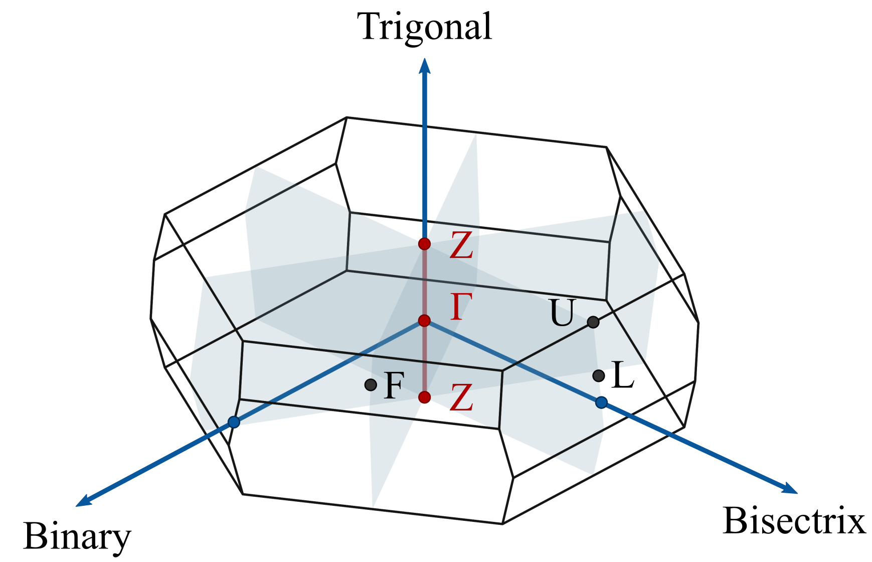
As compared to Bi2Se3 and Bi2Te3, the bulk band structure of Sb2Te3 remains to a great extent uncovered. The quantum oscillations experiments have so far been performed only on -type samples with rather high hole concentrations (above cm-3). The interpretation suggested six-fold [12, 13, 14, 15, 16] or twelve-fold [17] valley degeneracy, but also a more complex structure of the valence band, with six- and non-degenerated valleys combined [18]. While the single-valley degeneracy is connected with the center of the Brillouin zone (BZ) only, the sixfold degenerated band extrema may be located along the binary axes, or in the mirror planes, see Fig. 1.
The band structure of Sb2Te3 has been also several times addressed theoretically [19, 3, 20, 21, 22, 23]. The results of various ab-initio approaches are not fully consistent, but at least indicate that the band extrema should be primarily searched at the point, along the line or in the mirror planes. Notably, the calculated energies of different conduction or valence band extrema often differ only by several tens of meV. This is likely beyond the precision of theoretical methods and calls for a detailed experimental inspection that may allow us to determine the location, width and type of the fundamental band gap of Sb2Te3.
In this paper, we present a combined experimental and theoretical study of bulk electronic states in the Sb2Te3 topological insulator. Using magneto-optical, optical and magneto-transport methods, we find that Sb2Te3 is a material with a direct energy band gap. This gap reaches meV and it is located in the center of the BZ or along the trigonal axis. Nevertheless, the valence and conduction bands display also other local extrema at low energies, most likely in the mirror planes, and therefore, with a six-fold degeneracy.
II Sample preparation, experimental and computational details
The studied Sb2Te3 epilayer with a nominal thickness of nm (ellipsometry value: 276 nm) was grown using molecular beam epitaxy on a 1-mm-thick (111)-oriented cleaved BaF2 substrate. Compound Sb2Te3 and elemental Te sources were used for the control of the stoichiometry and composition. The deposition was carried out at a sample temperature of 290∘C at which a perfect 2D growth mode occurs as evidenced by reflection high energy electron diffraction and atomic force microscopy. The grown Sb2Te3 layer has the trigonal axis oriented perpendicular to the substrate.
The prepared epilayer was characterized using -ray diffraction measurements in the temperature range of 77-300 K. At room temperature, the deduced lattice constants, nm and nm, compare well to values reported in literature [24]: nm and nm, respectively. This suggests that the epilayer is well relaxed. The experiments also show that, when cooling down, a weak tensile stress (around 0.05%) appears as a result of different thermal contractions in BaF2 and Sb2Te3.
To measure infrared magneto-transmission, radiation from a globar or a mercury lamp was analyzed by a commercial Bruker Vertex 80v Fourier-transform spectrometer. The radiation was then delivered via light-pipe optics to the sample kept in the helium exchange gas at the temperature or 4.2 K and placed in a superconducting solenoid, or in the resistive high-field magnet (below or above 16 T, respectively), both at the LNCMI in Grenoble.

Infrared radiation transmitted through the sample was detected by a composite bolometer, placed below the sample. The studied sample was probed in both Faraday and Voigt configurations, with the wave vector propagating along and perpendicular to the applied magnetic field, respectively. In the latter case, a linear polarizer was used to select the electric polarization oriented perpendicularly to the applied magnetic field. The measured transmission spectra, , were normalized by the zero-field transmission, , and plotted in the form of relative magneto-transmission, , or alternatively, as relative magneto-absorbance, .
The optical response at was deduced using ellipsometry technique, using a commercial Woollam IR-VASE ellipsometer coupled to a closed He-cycle cryostat, for details see Ref. 26. Complementary magneto-transport measurements were realized using the standard lock-in technique on a sample with electrical contacts in the Hall-bar configuration, placed in the variable temperature insert in a superconducting coil (up to 16 T).
The first-principles calculations were carried out with density functional theory (DFT) and the approximation, as implemented in the code SPEX [27] within the FLAPW formalism (Full Potential Linearized Augmented Plane Waves). We used the same lattice parameters of Ref. [23]. The DFT calculations were performed using the exchange-correlation functional GGA-PBE [28]. We used an angular momentum cut-off =10 and a plane-wave cutoff of 4.5 bohr-1. The BZ was sampled using an k-point mesh, both in the DFT and the calculations.
A mixed product basis was used for the calculations, with an angular momentum cut-off of 5 and linear momentum cutoff of 2.9 bohr-1. The number of bands was set to 500 for the calculation of the Green function and the polarization function. The spin-orbit coupling (SOC) effect was incorporated with the method of Refs. [29, 30], which ensured that the SOC effects were fully included in the Green function, the screened Coulomb potential, and the self-energy.
The k-mesh used in the DFT and calculations ensures [23] that accurate Maximally Localized Wannier Functions (MLWFs) [31] can be constructed. This was done with the help of the WANNIER90 library [32]. Using the Wannier-interpolation technique as discussed in Ref. [23], one can obtain (interpolated) energy eigenvalues (DFT or ) in a denser mesh. We have used it to interpolate the eigenvalues in a mesh needed to converge the dielectric function. The latter was calculated from the RPA (Random Phase Approximation) polarizability [27] taking the macroscopic average including local-field effects.
III Results and Discussion
III.1 Magneto-optics
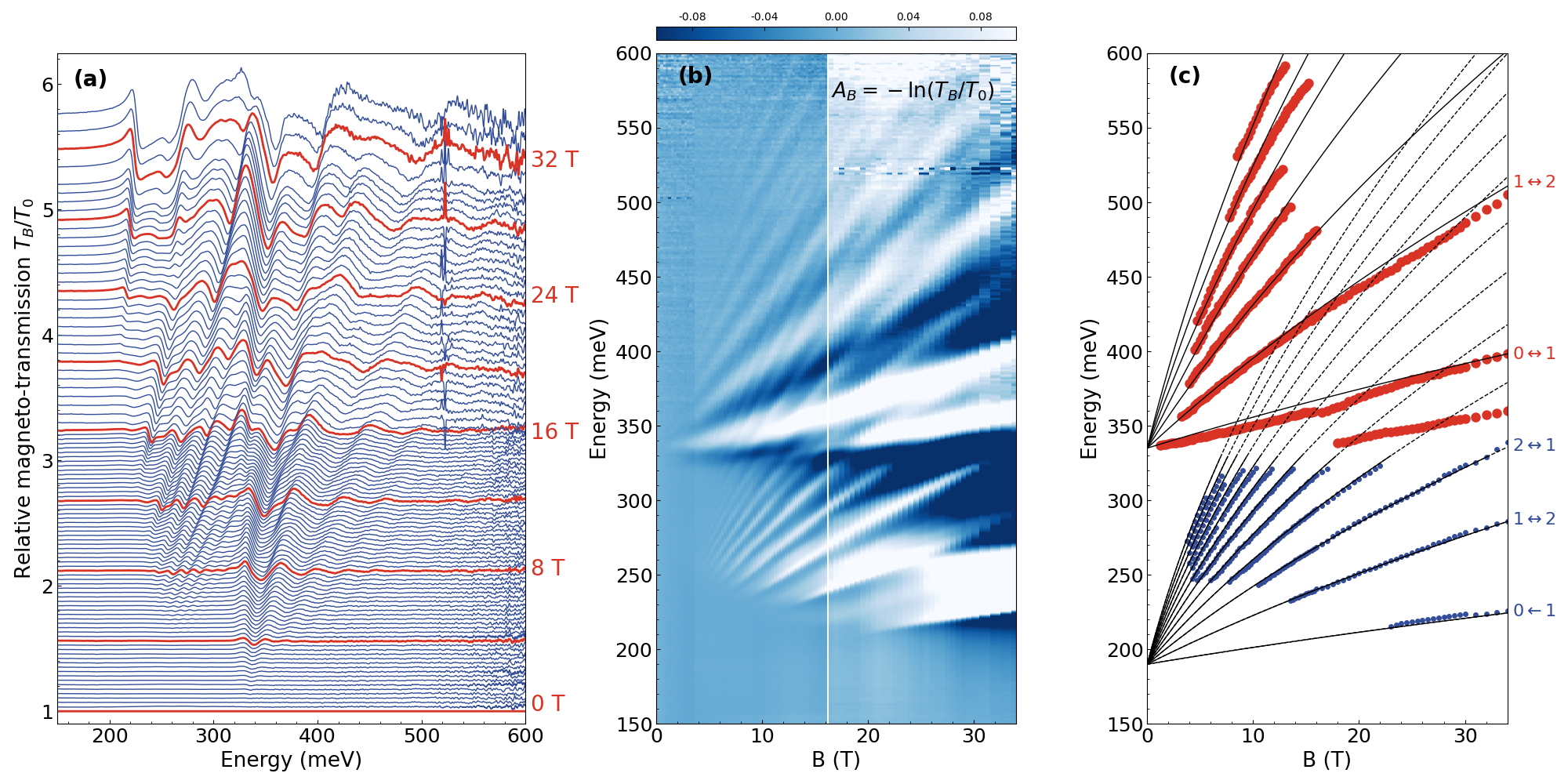
The magneto-optical data collected on the explored Sb2Te3 epilayer at low temperatures in the mid-infrared spectral range are presented in Fig. 2a and 2b as a stacked-plot of relative magneto-transmission spectra, , and as a false-color plot of relative magneto-absorbance, , respectively. The data are dominated by two series of resonances – by the upper and lower set – that may be directly associated with excitations bringing electrons across the band gap, between Landau-quantized valence bands. In our magneto-optical data, we did not identify any contribution directly attributable to surface states [6, 33, 34, 35].
Let us now analyze the observed transitions in terms of their position, -dependence and intensity, in a greater detail. The transitions in both series follow a weakly sub-linear in dependence and extrapolate to a finite photon energy in the limit of a vanishing magnetic field. Such behaviour is typical of narrow-gap semiconductors and can be, in this particular case, well reproduced using a simple two-band Hamiltonian often referred to as the model of massive Dirac electrons. In this simple model, with two material parameters only, the conduction (+) and valence (-) bands display hyperbolic profiles: , where is the velocity parameter and represents the width of the band gap. The magnetic field strong enough transforms these bands in dispersive one-dimensional Landau bands, with the band edge energies of , for .
Taking the standard selection rules for electric-dipole excitations, , the model reproduces the experimentally determined positions of interband inter-LL excitations very well, see Fig. 2c. For the lower set, the parameters read: meV and m/s. For the upper set, we obtained: meV and m/s. The extracted parameters allow us to get estimates of the band-edge masses, and , assuming that the electron-hole symmetry is preserved. stands for the bare electron mass.
Let us note that the successful application of the simplified, massive Dirac, model is to a certain extent surprising. Clearly, we deal with a topological insulator, and the lower series of inter-LL excitation is – as justified a posteriori in the paper – associated with the center of the BZ where the band structure is clearly inverted. In such a case, it is common to expand the Hamiltonian, to include a diagonal dispersive term which effectively describes the extension of the band inversion in the reciprocal space, see, e.g., Refs. [36, 37, 38, 39]. In the case of Sb2Te3, we were only able to set the upper limit for the inversion parameter: . For higher values, the theoretical -dependence of inter-LL excitations starts to deviate visibly from the experimental data. Another deviation from the simple massive Dirac model appears for the upper set in high magnetic fields. A satellite transition emerges at T below the line, which disperses approximately with the same slope. This additional line may correspond to an excitation from/to a shallow impurity state.
Other relevant pieces of information can be extracted from the intensity of excitations. Individual inter-LL transitions in the lower set emerge with increasing one-by-one, thus indicating a pronounced occupation effect. The quantum limit, with the Fermi energy in the lowest LL, is only achieved above 20 T when the transition appears in the response ( meV, see Fig. 2b). In fact, this is a well-known Moss-Burstein shift [40, 41], but with the onset of interband absorption driven by the -dependent Fermi energy. This implies that the lower set of transitions comes from a particular location in the BZ with a non-negligible density of free charge carriers. In contrast, no occupation effect is visibly manifested in the upper set which indicates a lower, or even negligible, carrier density in the concerned bands.
Magneto-optical experiments at lower photon energies, below the reststrahlenband of the BaF2 substrate, were performed as well, see Fig. 3. As expected, the transmission of the sample is low, due to absorption on free charge carriers (Drude-type). This takes a form of cyclotron resonance (CR) absorption when the magnetic field is applied. Unfortunately, the precise read-out of the CR energy and the extraction of the effective mass is not straightforward due to strong coupling, primarily due to a dielectric effect, between a pronounced phonon mode ( meV, see Ref. [25]) and free charge carriers. Nevertheless, a rough estimate of the effective mass from the -dependent minimum in the transmission response approaches the Dirac mass deduced for the lower set of interband excitations.
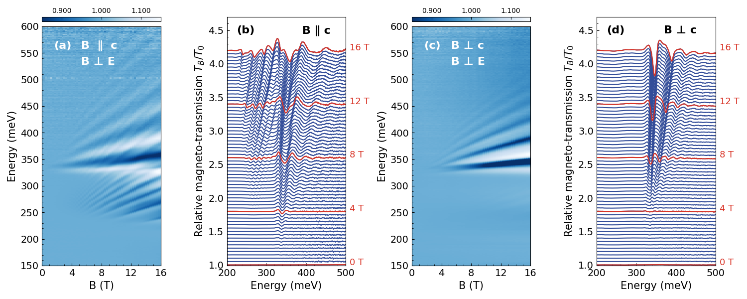
To probe the anisotropy of the magneto-optical response, a complementary magneto-optical experiment was carried out with oriented perpendicular to the trigonal axis of Sb2Te3 (). In the case of a thin layer, such an experiment is only possible in the Voigt configuration. To follow transitions active within the same set of selection rules as in the Faraday configuration, we used a linear polarizer and selected radiation with the electric field component perpendicular to the magnetic field (). The data collected in the Faraday and Voigt configuration are compared in Fig. 4.
Interestingly, the lower set of inter-LL excitations vanishes completely in the Voigt configuration (). This suggests a pronounced anisotropy of the band structure at the given location in the BZ. In contrast, the upper series of transitions shows nearly isotropic behaviour. Again, the observed response (i.e., the upper set) can be well reproduced using the model of massive Dirac electrons, with an identical band gap , but with the velocity parameter slightly lowered, m/s. Let us note that two independent experiments were realized in the Voigt configuration, with the sample rotated by 90 deg around the trigonal axis to probe the in-plane anisotropy. These measurements provide us with nearly identical results, consistent with a fairly low in-plane anisotropy (weak trigonal warping).
To sum up, the magneto-optical response of Sb2Te3 at low photon energies is surprisingly complex. It is dominated by two, or when the expected multiplicity of the band extrema is considered, more than two distinct locations in the BZ. These differ considerably in the extracted band gap, by the characteristic anisotropy of the local band structure, but also by the density of free charge carriers at the local band extrema. The observed magneto-optical response suggests that Sb2Te3 is a direct-gap semiconductor with the band gap reaching meV.
III.2 Magneto-transport
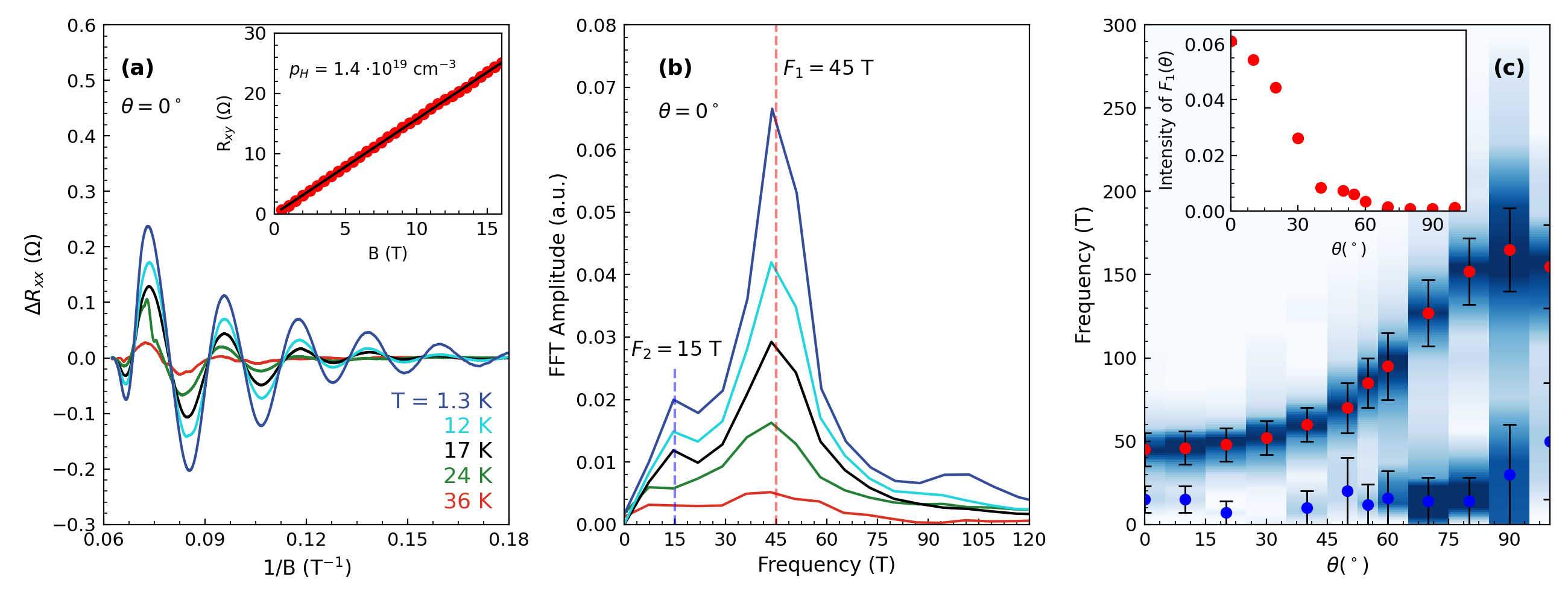
To complement our magneto-optical experiments, we performed a series of magneto-transport measurements on the same sample. Both transversal and longitudinal components of the magneto-resistivity tensor – with applied along the trigonal axis of Sb2Te3 – were recorded, the latter also as a function of temperature, see Fig. 5a. The Hall signal was linear in the applied magnetic field and the sign indicated -type conductivity typical of Sb2Te3 [12, 13, 14, 15, 16]. The slope corresponds to the total hole density of cm-3.
The longitudinal component exhibited well-visible Shubnikov-de Haas oscillations. Our analysis using the fast Fourier transformation indicated two oscillation periods, having frequencies of T and T, see Fig. 5b. This indicates the existence of two types of hole Fermi surfaces in our sample. Below, we refer to them as larger and smaller ones, respectively. Interestingly, no signs of splitting due to spin was observed. This may be surprising in a material with a particularly strong spin-orbit interaction. Nevertheless, in the sister material Bi2Se3, the same effect is present as well and explained as due to spin splitting that matches multiples of the cyclotron energy [42].
The Lifshitz-Kosevitch-like analysis of oscillations’ damping with temperature was only possible for the dominant oscillations, corresponding to the larger Fermi surface. It provided us with the effective mass of . When the approximation of a strictly parabolic band is used, this gives us an estimate of the Fermi energy around 40-50 meV.
To explore the anisotropy of the Fermi surfaces, we have also traced the Shubnikov-de Haas oscillations as a function of the angle between the trigonal axis and the direction of the applied magnetic field ( equiv. ). In our experiment, the magnetic field was oriented randomly with respect to the in-plane (-) crystallographic axes. The result of the frequency analysis is plotted in a form of a false-color plot in Fig. 5c.
Interestingly, the angle dependence is distinctively different for the two identified oscillation periods. The frequency , belonging to the larger Fermi surface, increases monotonically with the angle and reaches roughly 4 its original value at deg. This excludes the possibility that we observe the response of electrons in the surface states, recently reported on even thinner Sb2Te3 layers [43]. The amplitude of oscillations drops significantly, see the inset of Fig. 5c, becoming very weak at angles around deg. The larger Fermi surface is thus profoundly elongated in the direction of the trigonal axis. The frequency – corresponding to the smaller Fermi surface – remains constant as a function of within the experimental accuracy, and hence, this Fermi surface is approximately spherical. Let us note that a different angle dependence was observed in early magneto-transport studies of Sb2Te3. The observed oscillation period did not evolve monotonically with [12] and even signs of splitting appeared when was not parallel with the trigonal axis [17]. Such behavior was interpreted as due to the multiple-valley structure of the topmost valence band (with the valley degeneracy or 12). It is important to note, however, that those studies were performed on crystals with almost an order of magnitude larger hole density (around 1020 cm-3).

Having quantified the anisotropy of the larger Fermi surface, we may estimate the related per-valley density of holes. Let us assume that the band, even though profoundly anisotropic, has still a strictly parabolic profile at the concerned energies. The observed angle dependence of implies a relatively large difference – by a factor of 16 – between the effective masses perpendicular to and along the trigonal axis: and , respectively. This allows us to estimate, taking the frequency T at , the corresponding hole density per valley: cm-3.
The extracted per-valley hole density represents a half of the total hole density estimated in the Hall experiments. Even though there exists some uncertainty in the Hall read-out of the carrier density in systems with two types of charge carriers, this suggests that the larger hole pocket might be located at the point. Alternatively, the double valley degeneracy, , with two larger hole pockets located along the trigonal axis (along the line) is also possible. A higher valley degeneracy, or even , is not consistent with our findings since .
The extracted properties of the larger hole pocket, i.e., the anisotropy, effective mass, and the Fermi energy, remarkably resemble the analogous parameters deduced for the lower set of interband inter-LL transitions in Fig. 2. Hence, it is plausible to assume that they have their origin in the very same location of the BZ. This implies that the fundamental direct band gap of Sb2Te3 is located at the point () or alternatively along the line (), cf. Fig. 1.
Assigning the larger Fermi surface, observed in magneto-transport experiments, to the center of the BZ, one may speculate about the location(s) of the smaller one(s). It is plausible to assume that they may be located away from the trigonal axis – on the binary axis, in the mirror place (both ) or in a general location lacking any higher symmetry (). Most likely, those were the hole pockets which dominated the response in early quantum oscillation experiments performed on samples with a significantly higher hole density [12, 17].
III.3 Ellipsometry measurements
Let us now confront our conclusions so far with the result of the ellipsometry experiments. These were performed at and at varying : from room temperature down to 7 K. The deduced real part of optical conductivity, the optical constant most relevant for this work, is plotted in Fig. 6. It has a double-step onset at low photon energies, which smears out with the increasing temperature. To estimate the positions of these two onsets, we used the critical point model [44] and searched for zero-points in the second derivative of the imaginary part of the dielectric function (plotted in the top part of Fig. 6). The positions of onsets are marked by two vertical dashed lines at 277 and 329 meV in Fig. 6.
The lower inflection point matches well the expected onset of interband absorption at the point (or along the trigonal axis), corresponding to the fundamental band gap enhanced by twice the Fermi energy at the larger hole pocket: . This is due to the above mentioned Moss-Burstein shift [40, 41] typical of degenerate semiconductors with a low electron-hole asymmetry. The upper inflection point corresponds well to the onset of interband absorption at the energy of the local band gap . It is worth noting that, apart from smearing clearly visible in the spectra, the basic character of the zero-field optical response does not change with an increasing temperature. This implies that the band structure is robust against small temperature-induced strain/stress observed in the -ray diffraction experiments.
It is instructive to compare the zero-field optical response of Sb2Te3 with sibling materials: Bi2Se3 and Bi2Te3, in which the valley degeneracy of the fundamental band gap is consensually established: and , respectively. Interestingly, the profile of interband absorption in Bi2Se3 resembles – by its shape and amplitude – the first step in the absorption of Sb2Te3, just shifted towards higher energies. On the other hand, at higher photon energies, the optical conductivity of Bi2Te3 has the profile and overall strength similar to Sb2Te3, only shifted towards lower energies.
The above considerations are qualitative only, but they are in line with the above concluded single, or at most, double valley degeneracy of the fundamental direct band gap of meV in Sb2Te3. In addition, they point towards the sixfold valley degeneracy of the upper (local) band gap of meV. We suggest that this local band gap can be associated with the smaller hole pocket (the frequency ) observed in magneto-transport experiments.
| Material | Direct band | Location in | Valley | Effective band-edge |
|---|---|---|---|---|
| gap (meV) | Brillouin zone | degeneracy | mass | |
| Sb2Te3 | (or ) | 1 (or 2) | plane: | |
| axis: | ||||
| Mirror planes | 6 | |||
| Bi2Te3 [8] | Mirror planes | 6 |
III.4 Comparison with output of calculations
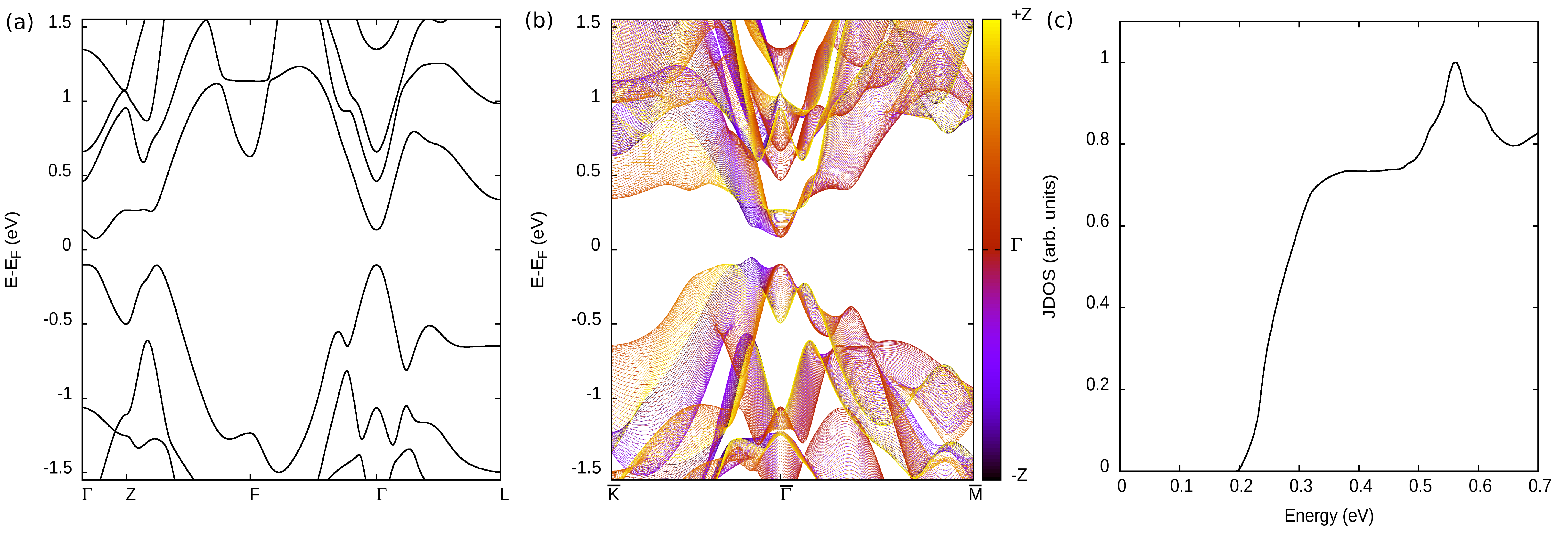
Let us now compare our inferences – made so far solely via the analysis of the experimental data – with the electronic band structure calculated using the approach. The band structure obtained theoretically along the selected directions of the BZ is plotted in Fig. 7a. A series of band structure cuts in the planes perpendicular to the (trigonal) axis, for selected values of , is presented in Fig. 7b. In Fig. 7c, the joint density of states calculated using the theoretical band structure is shown.
In the big picture, the calculated band structure is in a very good agreement with our conclusions based solely on the experimental data. The extrema of electronic bands relevant for low-energy excitations targeted in our experiments are indeed located at the point, along the line and in the mirror planes. The calculations suggest the existence of two nearly degenerate maxima of the topmost valence band. The predicted band gap is slightly below 200 meV, a value perfectly in line with our magneto-optical data (). The calculations also suggest fairly large anisotropy (in the direction along versus perpendicular to the trigonal axis) of the global valence band maximum at the point. In addition, the calculated step-like nature of the joint density of states (Fig. 7c) compares rather well with the onset of interband absorption visualized by ellipsometry experiments (Fig. 6).
Having said this, let us compare the experimental findings with theoretical predictions in a greater detail, to identify the existing differences. While our transport experiments on the -type sample conclude at most a double degeneracy of the global valence-band maximum, a sixfold degeneracy is suggested by calculations (Fig. 7b). This discrepancy is also related to another difference: The calculations imply an indirect type of the band gap, while the experimental data are rather consistent with a direct one. Both discrepancies have the same origin: the theoretical prediction of the two maxima in the valence band with similar energies. The highest one (the absolute valence band maximum) lies on the mirror plane (degeneracy ). The second one, approximately 40 meV below, is at the point (degeneracy ). However, as we discussed in Ref. [22], the relative energy between these two maxima is extremely sensitive to the details of the calculations. For example, a different set of lattice parameters used in the calculation can shift the valence band maximum from one position to the other (see Fig. 2 of Ref. [22]). Therefore, in this case, the band structure calculations cannot give a definitive answer about which of the two is the absolute maximum.
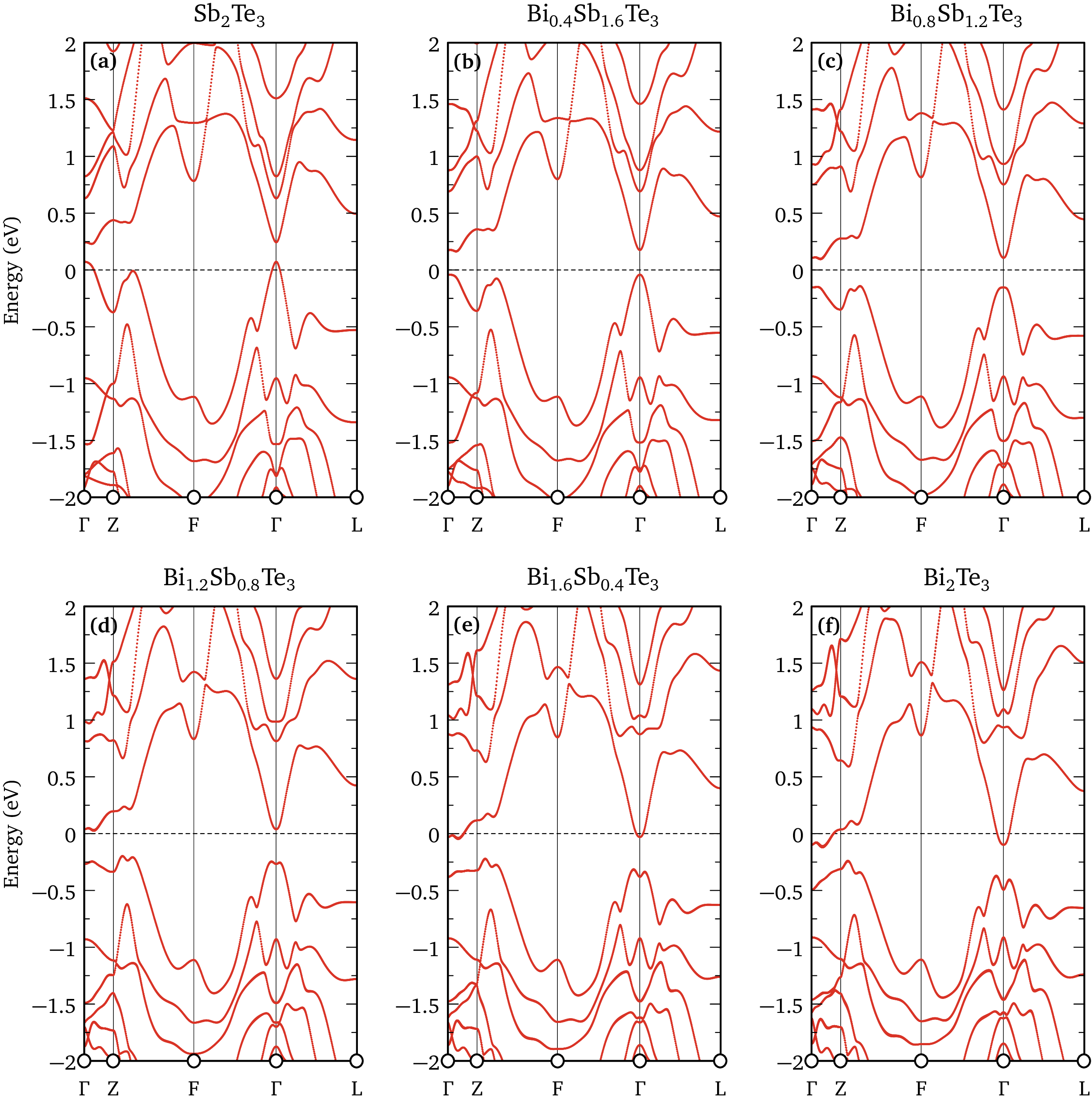
It is interesting to compare these findings to the band structure of the sister compound Bi2Te3. There, a consensus exists in literature, both in experimental studies [10, 8] and in theoretical calculations, that the valence band is characterized by six pronounced global maxima located in the mirror planes (). The results of calculations performed for the mixed compound (Sb1-xBiTe3 show such a trend when the Sb-to-Bi ratio increases, see Fig. 8 in the Appendix. Namely, the gradual increase in the bismuth concentration suppresses the valence band maximum at the point and enhances the maxima in the mirror planes (- direction). These latter maxima become the global ones for . This picture is also consistent with conclusions of early quantum-oscillation experiments performed on the mixed (Sb1-xBiTe3 crystals [13]. The comparison of band structure parameters deduced in this work for Sb2Te3 with those for Bi2Te3 [8] is made in Tab. 1.
Finally, we have experimentally shown that, besides the fundamental band gap in the centre of the BZ, the band structure comprises also additional, local energy band gaps, located most likely in the mirror planes and with fairly high, in their vicinity, isotropic bands. However, these additional band gaps are not clearly identified in our calculations. Even though, such a maximum of the calculated topmost valence band can be found in the mirror plane, the shape of rather shallow counterpart in the conduction band would not allow to form a well-defined Landau quantization at the scale seen in our experimental data.
IV Conclusions
We conclude that antimony telluride is a semiconductor with a direct energy band gap of meV at low temperatures, which is located at the center of the BZ, or alternatively, along the trigonal axis. In the observed response, we do also identify additional local maxima of the valence band, nearly degenerate with the global one, which form additional (local) direct gaps with the width of meV and displaying the six-fold valley degeneracy (mirror planes). Our findings are in fairly good agreement with the electronic band structure calculated using the method, thus demonstrating high predictive power of this advanced theoretical technique.
Acknowledgements.
The authors also acknowledge the support of the LNCMI-CNRS in Grenoble, a member of the European Magnetic Field Laboratory (EMFL). The work has been supported by the ANR projects DIRAC3D (ANR-17-CE30-0023) and COLECTOR (ANR-19-CE30-0032). This research was supported by the NCCR MARVEL, a National Centre of Competence in Research, funded by the Swiss National Science Foundation (grant number 205602). IA and MFT acknowledge the computing time granted through SURF on the Dutch National Supercomputer Snellius. X.S. and B.P. acknowledge support from ANR Grant No. ANR-20-CE30-0015-01. This work was supported by the project Quantum materials for applications in sustainable technologies (QM4ST), funded as project No. CZ.02.01.01/00/22_008/0004572 by P JAK, call Excellent Research.*
Appendix A Electronic band structure of (Sb1-xBiTe3
Figure 8 show the electronic band structure of (Sb1-xBiTe3 calculated theoretically for several material’s compositions: and 1. These were calculated following the approach described in Ref. [23]. We constructed Wannier tight-binding Hamiltonians fully from first-principles from the GW (”GW-TB”) calculations of the parent compounds Sb2Te3 and Bi2Te3. We used a 666 k-point mesh for these calculations. The alloys were achieved by the use of the virtual crystal approximation (VCA) starting from the two GW-TB Hamiltonians of the binary compounds. The doping was simulated for the parent compounds by fitting the calculated band extrema to the ARPES results from [45].
References
- Hasan and Kane [2010] M. Z. Hasan and C. L. Kane, Colloquium: Topological insulators, Rev. Mod. Phys. 82, 3045 (2010).
- Qi and Zhang [2011] X.-L. Qi and S.-C. Zhang, Topological insulators and superconductors, Rev. Mod. Phys. 83, 1057 (2011).
- Zhang et al. [2009] H. Zhang, C.-X. Liu, X.-L. Qi, X. Dai, Z. Fang, and S.-C. Zhang, Topological insulators in Bi2Se3, Bi2Te3 and Sb2Te3 with a single Dirac cone on the surface, Nature Phys. 5, 438 (2009).
- Hsieh et al. [2009a] D. Hsieh, Y. Xia, D. Qian, L. Wray, J. Dil, F. Meier, J. Osterwalder, L. Patthey, J. Checkelsky, N. P. Ong, et al., A tunable topological insulator in the spin helical Dirac transport regime, Nature 460, 1101 (2009a).
- Chen et al. [2009] Y. L. Chen, J. G. Analytis, J.-H. Chu, Z. K. Liu, S.-K. Mo, X. L. Qi, H. J. Zhang, D. H. Lu, X. Dai, Z. Fang, S. C. Zhang, I. R. Fisher, Z. Hussain, and Z.-X. Shen, Experimental realization of a three-dimensional topological insulator, Bi2Te3, Science 325, 178 (2009).
- Hsieh et al. [2009b] D. Hsieh, Y. Xia, D. Qian, L. Wray, F. Meier, J. H. Dil, J. Osterwalder, L. Patthey, A. V. Fedorov, H. Lin, A. Bansil, D. Grauer, Y. S. Hor, R. J. Cava, and M. Z. Hasan, Observation of time-reversal-protected single-Dirac-cone topological-insulator states in and , Phys. Rev. Lett. 103, 146401 (2009b).
- Orlita et al. [2015] M. Orlita, B. A. Piot, G. Martinez, N. K. S. Kumar, C. Faugeras, M. Potemski, C. Michel, E. M. Hankiewicz, T. Brauner, C. Drašar, S. Schreyeck, S. Grauer, K. Brunner, C. Gould, C. Brüne, and L. W. Molenkamp, Magneto-optics of massive Dirac fermions in bulk Bi2Se3, Phys. Rev. Lett. 114, 186401 (2015).
- Mohelský et al. [2020] I. Mohelský, A. Dubroka, J. Wyzula, A. Slobodeniuk, G. Martinez, Y. Krupko, B. A. Piot, O. Caha, J. Humlíček, G. Bauer, G. Springholz, and M. Orlita, Landau level spectroscopy of Bi2Te3, Phys. Rev. B 102, 085201 (2020).
- Köhler [1976a] H. Köhler, Non-parabolic relation of the lowest conduction band in Bi2Te3, phys. stat. sol. (b) 73, 95 (1976a).
- Köhler [1976b] H. Köhler, Non-parabolicity of the highest valence band of Bi2Te3 from Shubnikov-de Haas effect, phys. stat. sol. (b) 74, 591 (1976b).
- Köhler [1976c] H. Köhler, Anisotropic -factor of the conduction electrons in Bi2Te3, phys. stat. sol. (b) 75, 127 (1976c).
- Schwartz et al. [1967] H. Schwartz, G. Björck, and O. Beckman, De Haas - van Alphen susceptibility measurements on -type Sb2Te3, Solid State Commun. 5, 905 (1967).
- Köhler and Freudenberger [1977] H. Köhler and A. Freudenberger, Investigation of the highest valence band in (Bi1-xSbx)2Te3 crystals, phys. stat. sol. (b) 84, 195 (1977).
- Kulbachinskii et al. [1995] V. A. Kulbachinskii, Z. M. Dashevskii, M. Inoue, M. Sasaki, H. Negishi, W. X. Gao, P. Lostak, J. Horak, and A. de Visser, Valence-band changes in and by transport and Shubnikov–de Haas effect measurements, Phys. Rev. B 52, 10915 (1995).
- Zhao et al. [2019] W. Zhao, D. Cortie, L. Chen, Z. Li, Z. Yue, and X. Wang, Quantum oscillations in iron-doped single crystals of the topological insulator , Phys. Rev. B 99, 165133 (2019).
- Kulbachinskii et al. [2021] V. Kulbachinskii, D. Zinoviev, V. Kytin, M. Mikhailov, and Z. Ismailov, Thermoelectical properties and Shubnikov - de Haas effect in single crystals Sb2-xCuxTe3, Materials Today: Proceedings 44, 3439 (2021), 17th European Thermoelectric Conference.
- von Middendorff et al. [1973] A. von Middendorff, K. Dietrich, and G. Landwehr, Shubnikov-de Haas effect in -type Sb2Te3, Solid State Commun. 13, 443 (1973).
- Simon and Eichler [1981] G. Simon and W. Eichler, Investigations on a two-valence band model for Sb2Te3, phys. stat. sol. (b) 107, 201 (1981).
- Wang and Cagin [2007] G. Wang and T. Cagin, Electronic structure of the thermoelectric materials and from first-principles calculations, Phys. Rev. B 76, 075201 (2007).
- Yavorsky et al. [2011] B. Y. Yavorsky, N. F. Hinsche, I. Mertig, and P. Zahn, Electronic structure and transport anisotropy of Bi2Te3 and Sb2Te3, Phys. Rev. B 84, 165208 (2011).
- Aguilera et al. [2013a] I. Aguilera, C. Friedrich, G. Bihlmayer, and S. Blügel, study of topological insulators Bi2Se3, Bi2Te3, and Sb2Te3: Beyond the perturbative one-shot approach, Phys. Rev. B 88, 045206 (2013a).
- Nechaev et al. [2015] I. A. Nechaev, I. Aguilera, V. De Renzi, A. di Bona, A. Lodi Rizzini, A. M. Mio, G. Nicotra, A. Politano, S. Scalese, Z. S. Aliev, M. B. Babanly, C. Friedrich, S. Blügel, and E. V. Chulkov, Quasiparticle spectrum and plasmonic excitations in the topological insulator , Phys. Rev. B 91, 245123 (2015).
- Aguilera et al. [2019] I. Aguilera, C. Friedrich, and S. Blügel, Many-body corrected tight-binding hamiltonians for an accurate quasiparticle description of topological insulators of the family, Phys. Rev. B 100, 155147 (2019).
- Anderson and Krause [1974] T. L. Anderson and H. B. Krause, Refinement of the Sb2Te3 and Sb2Te2Se structures and their relationship to nonstoichiometric Sb2Te3-ySey compounds, Acta Crystallographica Section B 30, 1307 (1974).
- Bragaglia et al. [2020] V. Bragaglia, M. Ramsteiner, D. Schick, J. E. Boschker, R. Mitzner, R. Calarco, and K. Holldack, Phonon anharmonicities and ultrafast dynamics in epitaxial Sb2Te3, Sci. Rep. 10, 12962 (2020).
- Dubroka et al. [2017] A. Dubroka, O. Caha, M. Hronček, P. Friš, M. Orlita, V. Holý, H. Steiner, G. Bauer, G. Springholz, and J. Humlíček, Interband absorption edge in the topological insulators Bi2(Te1-xSex)3 , Phys. Rev. B 96, 235202 (2017).
- Friedrich et al. [2010] C. Friedrich, S. Blügel, and A. Schindlmayr, Efficient implementation of the approximation within the all-electron flapw method, Phys. Rev. B 81, 125102 (2010).
- Perdew et al. [1996] J. P. Perdew, K. Burke, and M. Ernzerhof, Generalized gradient approximation made simple, Phys. Rev. Lett. 77, 3865 (1996).
- Aguilera et al. [2013b] I. Aguilera, C. Friedrich, and S. Blügel, Spin-orbit coupling in quasiparticle studies of topological insulators, Phys. Rev. B 88, 165136 (2013b).
- Sakuma et al. [2011] R. Sakuma, C. Friedrich, T. Miyake, S. Blügel, and F. Aryasetiawan, calculations including spin-orbit coupling: Application to Hg chalcogenides, Phys. Rev. B 84, 085144 (2011).
- Marzari et al. [2012] N. Marzari, A. A. Mostofi, J. R. Yates, I. Souza, and D. Vanderbilt, Maximally localized Wannier functions: Theory and applications, Rev. Mod. Phys. 84, 1419 (2012).
- Mostofi et al. [2008] A. A. Mostofi, J. R. Yates, Y.-S. Lee, I. Souza, D. Vanderbilt, and N. Marzari, wannier90: A tool for obtaining maximally-localised Wannier functions, Comput. Phys. Commun. 178, 685 (2008).
- Zhu et al. [2015] S. Zhu, Y. Ishida, K. Kuroda, K. Sumida, M. Ye, J. Wang, H. Pan, M. Taniguchi, S. Qiao, S. Shin, and A. Kimura, Ultrafast electron dynamics at the Dirac node of the topological insulator Sb2Te3, Sci. Rep. 5, 13213 (2015).
- Lund et al. [2021] H. E. Lund, K. Volckaert, P. Majchrzak, A. J. H. Jones, M. Bianchi, M. Bremholm, and P. Hofmann, Bulk band structure of Sb2Te3 determined by angle-resolved photoemission spectroscopy, Phys. Chem. Chem. Phys. 23, 26401 (2021).
- Locatelli et al. [2022] L. Locatelli, A. Kumar, P. Tsipas, A. Dimoulas, E. Longo, and R. Mantovan, Magnetotransport and ARPES studies of the topological insulators Sb2Te3 and Bi2Te3 grown by MOCVD on large-area Si substrates, Sci. Rep. 12, 3891 (2022).
- Liu et al. [2010] C.-X. Liu, X.-L. Qi, H. Zhang, X. Dai, Z. Fang, and S.-C. Zhang, Model Hamiltonian for topological insulators, Phys. Rev. B 82, 045122 (2010).
- Assaf et al. [2016] B. A. Assaf, T. Phuphachong, V. V. Volobuev, A. Inhofer, G. Bauer, G. Springholz, L. A. de Vaulchier, and Y. Guldner, Massive and massless Dirac fermions in Pb1-xSnxTe topological crystalline insulator probed by magneto-optical absorption, Sci. Rep. 6, 20323 (2016).
- Ly and Basko [2016] O. Ly and D. M. Basko, Theory of electron spin resonance in bulk topological insulators bi2se3, bi2te3and sb2te3, Journal of Physics: Condensed Matter 28, 155801 (2016).
- Tikuišis et al. [2021] K. K. Tikuišis, J. Wyzula, L. Ohnoutek, P. Cejpek, K. Uhlířová, M. Hakl, C. Faugeras, K. Výborný, A. Ishida, M. Veis, and M. Orlita, Landau level spectroscopy of the PbSnSe topological crystalline insulator, Phys. Rev. B 103, 155304 (2021).
- Burstein [1954] E. Burstein, Anomalous optical absorption limit in InSb, Phys. Rev. 93, 632 (1954).
- Moss [1954] T. S. Moss, The interpretation of the properties of indium antimonide, Proc. Phys. Soc. B 67, 775 (1954).
- Köhler and Wöchner [1975] H. Köhler and E. Wöchner, The -factor of the conduction electrons in Bi2Se3, phys. stat. sol. (b) 67, 665 (1975).
- Weyrich et al. [2017] C. Weyrich, T. Merzenich, J. Kampmeier, I. E. Batov, G. Mussler, J. Schubert, D. Grützmacher, and T. Schäpers, Magnetoresistance oscillations in MBE-grown Sb2Te3 thin films, Appl. Phys. Lett. 110, 092104 (2017).
- Yu and Cardona [1996] P. Y. Yu and M. Cardona, Fundamentals of semiconductors: physics and materials properties (Springer, 1996).
- Eschbach et al. [2015] M. Eschbach, E. Młyńczak, J. Kellner, J. Kampmeier, M. Lanius, E. Neumann, C. Weyrich, M. Gehlmann, P. Gospodarič, S. Döring, G. Mussler, N. Demarina, M. Luysberg, G. Bihlmayer, T. Schäpers, L. Plucinski, S. Blügel, M. Morgenstern, C. M. Schneider, and D. Grützmacher, Realization of a vertical topological p–n junction in epitaxial Sb2Te3/Bi2Te3 heterostructures, Nature Comm. 6, 8816 (2015).