Manipulating Topological Properties in Bi2Se3/BiSe/TMDC Heterostructures with Interface Charge Transfer
Abstract
Heterostructures of topological insulator Bi2Se3 on transition metal dichalcogenides (TMDCs) offer a new materials platform for studying novel quantum states by exploiting the interplay among topological orders, charge orders and magnetic orders. The diverse interface attributes, such as material combination, charge re-arrangement, defect and strain, can be utilized to manipulate the quantum properties of this class of materials. Recent experiments of Bi2Se3/NbSe2 heterostructures show signatures of strong Rashba band splitting due to the presence of a BiSe buffer layer, but the atomic level mechanism is not fully understood. We conduct first-principles studies of the Bi2Se3/BiSe/TMDC heterostructures with five different TMDC substrates (1T phase VSe2, MoSe2, TiSe2, and 2H phase NbSe2, MoSe2). We find significant charge transfer at both BiSe/TMDC and Bi2Se3/BiSe interfaces driven by the work function difference, which stabilizes the BiSe layer as an electron donor and creates interface dipole. The electric field of the interface dipole breaks the inversion symmetry in the Bi2Se3 layer, leading to the giant Rashba band splitting in two quintuple layers and the recovery of the Dirac point in three quintuple layers, with the latter otherwise only occurring in thicker samples with at least six Bi2Se3 quintuple layers. Besides, we find that strain can significantly affect the charge transfer at the interfaces. Our study presents a promising avenue for tuning topological properties in heterostructures of two-dimensional materials, with potential applications in quantum devices.
I INTRODUCTION
Topological insulators (TIs) [1, 2, 3, 4] are materials that are insulating in bulk but conducting on the surface. The Dirac surface states (DSSs) of TIs are protected by time-reversal symmetry and exhibit a characteristic spin-momentum locking with a linear dispersion relation. These properties make TIs attractive for various applications in spintronics [5], quantum computing [6], optoelectronics [7, 8], and thermoelectrics [9, 10]. The interplay among topological orders, charge orders (e.g. superconductivity and charge density wave) and magnetic orders can create exotic quantum states, which has drawn great interest in recent research [11, 12, 13, 14, 15, 16].
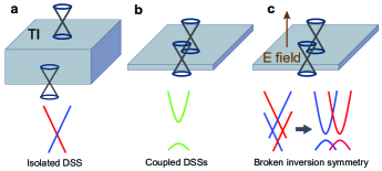
Heterostructures of two-dimensional (2D) materials or thin films bounded by van der Waals (vdW) forces are a fascinating playground for realizing new quantum materials. In particular, interface properties, such as the combination of materials, defects, strain and charge rearrangement, provide a wide, tunable design space to achieve new quantum properties [17, 18, 19]. In this study, we demonstrate that interface charge transfer in vdW heterostructures can be used to tune DSSs of TIs, as shown in the schematics in Fig. 1.
In bulk TIs, the top and bottom DSSs are degenerate in energy, but isolated in real space (Fig. 1a). However, in thin film TIs, the DSSs can couple and open a gap [20] (Fig. 1b). In the bulk to 2D transition, the Dirac points and the corresponding spin-momentum locking are destroyed, which limits the application of thin film TIs in quantum information science. We propose to separate the top and bottom DSSs in thin film TIs in the energy domain by applying an out-of-plane electric field, which could arise from an interface dipole layer as a result of charge transfer. The electric field creates a potential energy offset in the two DSSs, which can still couple and open a gap. Two Dirac points re-emerge at different energies as the result of the inversion symmetry breaking and the strong Rashba spin-orbit coupling (SOC) in thin film TIs (Fig. 1c). In this study, we focus on the realization of this mechanism using bismuth selenide (Bi2Se3) and transition metal dichalcogenide (TMDC) heterostructures.
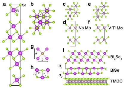
Bi2Se3 is one of the most studied three-dimensional (3D) TIs [21, 22, 23]. It has a layered structure consisting of quintuple layers (QLs) of Se-Bi-Se-Bi-Se atoms that are weakly bounded by vdW forces (Figs. 2a and 2b). Zhang et al. reported that the DSS disappears when Bi2Se3 thin films have less than 6 QLs [20], as the top and bottom DSSs couple and open a gap.
TMDCs are two-dimensional materials that have diverse electronic and optical properties, such as semiconducting, metallic, or superconducting behaviors [24, 25, 26, 27, 28]. Monolayer TMDCs have two types of structures: mirror symmetric 2H phase and inversion symmetric 1T phase as shown in Figs. 2c-2f. When Bi2Se3 is grown on TMDCs, novel topological properties can emerge depending on the interlayer coupling and the band alignment between the two materials.
Recent X-ray reflectivity (XRR) and X-ray diffraction (XRD) studies by Choffel et al. showed that when growing Bi2Se3 on metallic TMDCs, such as 2H phase of NbSe2 (2H-NbSe2) and 1T phase of TiSe2 (1T-TiSe2), VSe2 (1T-VSe2) and MoSe2 (1T-MoSe2), a buffer BiSe layer can form between them [29, 30]. Angle-resolved photoemission spectroscopy (ARPES) measurements revealed that the topological Dirac states reappear in the Bi2Se3/BiSe/NbSe2 heterostructure, when the thickness of Bi2Se3 is only 3 QLs accompanied by a giant Rashba band splitting [31], in contrast to the critical thickness of 6 QLs on SiC substrate [20]. In addition, a giant Rashba splitting is found in Bi2Se3 bands [31].
It has been suggested that the formation of the BiSe buffer layer is responsible for the observed novel topological properties in the Bi2Se3/BiSe/NbSe2 heterostructure. The BiSe buffer layer, similar to PbSe and LaSe, belongs to a rock-salt structured family that can form misfit layered compounds [32, 33, 34, 35, 36, 37, 38, 39] with TMDCs, including 1T-TiSe2, 2H-NbSe2 and 1T-VSe2. It has unique electronic properties such as one-dimensional electronic states [40]. More importantly, the misfit structure suppresses interlayer bonding while allowing charge transfer to dope neighboring layers and tune quantum states in the heterostructure. For example, the charge transfer between misfit layers has a strong impact on the charge density wave and superconductivity phase [41, 42].
The structure of the BiSe monolayer is shown in Figs. 2g and 2h. The isolated system is metallic with occupied antibonding states and thus tends to donate electrons to adjacent materials as in misfit materials (BiSe)1+δ/NbSe2 [43]. This property makes it a great candidate to modify the electronic properties of the interface. Besides, monolayer BiSe has a flexible structure that can grow on substrates with varying lattice constants. Scanning tunneling microscopy studies of the Bi2Se3/BiSe/NbSe2 heterostructure show that the BiSe buffer layer has a distorted square lattice with the in-plane Se-Bi-Se bond angle ( in Fig. 2h) becoming either acute or obtuse [44]. Density functional theory (DFT) calculations suggest that the isolated BiSe monolayer breaks the 4-fold rotation symmetry [45] characterized by two different lattice parameters ( and ) as shown in Fig. 2g.
In spite of its intriguing topological properties, the atomic level structural details and the electronic structure of Bi2Se3/BiSe/TMDC heterostructures have not been fully understood. Due to the lattice mismatch in the three materials, a large supercell with hundreds of atoms is needed to minimize the artificial strain when building the heterostructure, which requires significant computational power. Existing ab initio studies of Bi2Se3/BiSe/NbSe2 heterostructures consider an incomplete structure model, which contains only the Bi2Se3/BiSe interface [31]. In order to qualitatively reproduce the Rashba splitting in Bi2Se3, this model requires a prematurely terminated relaxation to avoid unphysical structure distortion in the absence of the NbSe2 layer [31], since the NbSe2 layer can play a crucial role in stabilizing the BiSe buffer layer. As such, a complete atomic scale physical picture of Bi2Se3/BiSe/TMDC heterostructures is still missing, and first-principles studies of the complete heterostructure are essential to gain insight into the atomic structure of the top and bottom interfaces, charge transfer characteristics, band alignment and topological properties of the Bi2Se3/BiSe/TMDC heterostructures.
In this study, we build a series of Bi2Se3/BiSe/TMDC models and conduct first-principles studies to reveal the origin of the giant Rashba splitting and Dirac crossing in few-QL Bi2Se3. We systematically investigate five hexagonal TMDC substrates (two 2H phase TMDCs: 2H-NbSe2 and 2H-MoSe2; three 1T phase TMDCs: 1T-TiSe2, 1T-VSe2 and 1T-MoSe2; see Figs. 2c-2f) that have been reported in the experimental studies of new misfit compounds [29, 30] and Rahsba superconductivity pairing [31]. Due to the rich electronic properties of TMDCs and the tunable strong Rashba SOC induced in Bi2Se3, the Bi2Se3/BiSe/TMDC heterostructures are promising material platforms for future quantum applications, such as realizing topological superconductors and performing topological quantum computing.
The rest of the paper is organized as follows. In Section II, we summarize the computational details. In Section III.1, we discuss the band alignment based on the work functions or electron affinity of heterostructure constituents. Then in Section III.2, we analyze the structure and stability of the BiSe buffer layer. In Section III.3, we quantify the amount of charge transfer at the interfaces. In Section III.4, we compare the calculated band structure of QL-Bi2Se3/BiSe/NbSe2 (=1,2 and 3) with ARPES measurements. Finally, we investigate the strain effect in Section III.5.
II METHODS
| TMDC | BiSe | Bi2Se3 | |
|---|---|---|---|
| 2H-NbSe2 | |||
| 1T-TiSe2 | |||
| XSe2111XSe2 represents 1T-VSe2 and 1T or 2H phase MoSe2. |
DFT calculations are performed using the projector-augmented-wave (PAW) method [46] implemented in the Vienna Ab initio Simulation Package (VASP) [47, 48, 49]. The exchange-correlation effects are treated under the generalized gradient approximation using the Perdew-Burke-Ernzerhof (PBE) functional [50]. The non-local vdW interaction is modeled by the vdW-D2 method [51].
Due to the lattice mismatch at the TMDC/BiSe and BiSe/Bi2Se3 interfaces, slab models of the heterostructures are built from supercells with 300 to 600 atoms as summarized in Table 1 (see also Fig. 2i and Supplemental Material [52]). The heterostructure models contain a TMDC monolayer, a BiSe monolayer and one to three QLs of Bi2Se3. Except for explicitly mentioned, 2QL-Bi2Se3 is used throughout this study. The lattice mismatch in the supercell is less than 1.5% between TMDC and Bi2Se3 and less than 4% between BiSe and Bi2Se3. To avoid the spurious interaction between periodic images of the slab, we include a vacuum region of at least 20 Å and apply the dipole correction [53] in the DFT calculations. The structure relaxation is performed by fixing the monolayer TMDC substrate and relaxing the rest of the system until the total energy difference is less than eV and the force is less than eV/Å.
To study the interface charge transfer, the electron density difference is calculated by subtracting the electron densities of isolated TMDCs, BiSe and Bi2Se3 from that of the heterostructure. The iso-surface plots are generated with the VASPKIT package [54]. The band structures of the heterostructures are computed including SOC and unfolded to the Bi2Se3 Brillouin zone using the Vaspbandunfolding package [55].
III Results and Discussion
III.1 Band alignment of the Bi2Se3/BiSe/TMDC heterostructures
The free-standing BiSe monolayer (see Figs. 2g and 2h) is unstable, because of the strong Coulomb repulsion from the excess electrons on the Bi atom (one per Bi atom). Our Bader charge analysis [56] shows that each Bi atom in BiSe has 0.3 electrons more than that in bulk Bi2Se3. As a result, the isolated BiSe monolayer favors the zigzag shape in the lateral direction rather than the rectangular shape (as shown from the side view in Fig. 2h), in order to maximize the Bi-Bi distance, with the Se-Bi-Se bond angle and the out-of-plane BiSe bond length Å. Due to the breaking of the 4-fold rotation symmetry [33], in-plane parameters ( Å and Å) have different values (see Fig. 2g). One practical strategy to stabilize the BiSe monolayer is to put it in contact with electron acceptors forming heterostructures [43]. Since the energy level alignment at the interface plays a critical role in determining the charge re-arrangement and the thermodynamic stability of the heterostructures, below we investigate the energy level alignment at the BiSe/TMDC and Bi2Se3/BiSe interfaces.
We calculate the work function () of the isolated monolayer BiSe and metallic monolayer TMDCs, as well as the electron affinity () of the isolated semiconducting monolayer TMDC and bulk Bi2Se3 as shown in Table 2. At the PBE level, eV, which is lower than that of all the metallic monolayer TMDCs, 1T-MoSe2 (4.52 eV), 1T-VSe2 (5.01 eV), 1T-TiSe2 (5.31 eV) and 2H-NbSe2 (5.52 eV), and of the semiconducting 2H-MoSe2 monolayer (3.90 eV). Our results show good agreement with the PBE calculations in the literature, e.g. 2H-NbSe2 (5.54 eV [57]), 1T-TiSe2 (5.35 eV [58]), 1T-VSe2 (5.05 eV [58]), 1T-MoSe2 (4.58 eV [58]), 2H-MoSe2 (3.86 eV [59]). They are in reasonable agreement with measured of the 1T-VSe2 monolayer (5.0 [60], 5.52 eV [61]) and of the semiconducting 2H-MoSe2 monolayer (3.5, 3.8 eV [62]).
Based on Table 2, at the BiSe/TMDC interface, or is larger than by up to 1.80 eV, which drives electron transfer from BiSe to TMDCs. At the Bi2Se3/BiSe interface, is lower than by 1.68 eV. Therefore, BiSe also donates electrons to Be2Se3. The charge transfer at both the top and bottom interfaces can significantly reduce the Coulomb repulsion of excess electrons in BiSe, which in turn can stabilize the BiSe buffer layer.
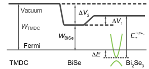
The charge transfer in the Bi2Se3/BiSe/TMDC heterostructures creates interface dipoles at both the top and bottom interfaces. The resulting dipole field shifts the vacuum potential, which determines the overall band alignment in the heterostructures. A qualitative picture is outlined in Fig. 3. As illustrated in this diagram, the band alignment at the BiSe/TMDC and Bi2Se3/BiSe interfaces is dominated by the dipole potential and , respectively. The relative position of the conduction band minimum (CBM) of Bi2Se3 () against the Fermi level is associated with through . We plot the Hartree potential of the 2QL-Bi2Se3/BiSe/NbSe2 heterostructure in Fig. S3 of the Supplemental Material [52]. The vacuum level difference of 0.33 eV between the bottom and top of the heterostructure corresponds to , as the net effect of the interface dipole. From the projected density of states (PDOS) of the Bi2Se3 bands, is estimated to be 0.44 eV. We note that and in the heterostructure (as shown in Fig. 3) can be slightly different from those of the isolated system due to structure distortion and charge re-arrangement. For example, in the 2QL-Bi2Se3/BiSe/NbSe2, Bi2Se3 has a slightly larger than the free-standing system by 3%.
| TMDCs | BiSe | Bi2Se3 | |||||
| 2H-NbSe2 | 1T-TiSe2 | 1T-VSe2 | 1T-MoSe2 | 2H-MoSe2 | |||
| DFT | 5.52 (5.54222See Ref. [57]) | 5.31(5.35333See Ref. [58]) | 5.01(5.053) | 4.52(4.583) | 3.90 (3.86444See Ref. [59]) | 3.72 | 5.40 |
| experiment | - | - | 5.0555See Ref. [60],5.52666See Ref. [61] | - | 3.5,3.8777(3.8 ± 0.1) eV on Al2O3/Si and (3.5 ± 0.1) eV on SiO2/Si. See Ref. [62] | - | - |
| TMDC | 2H-NbSe2 | 1T-TiSe2 | 1T-VSe2 | 1T-MoSe2 | 2H-MoSe2 |
|---|---|---|---|---|---|
| 2.75 | 2.79 | 2.77 | 2.80 | 2.82 | |
| 2.84 | 2.84 | 2.82 | 2.82 | 2.75 | |
| 3.08 | 3.06 | 3.08 | 3.05 | 2.98 | |
| 2.92 | 3.06 | 3.12 | 3.15 | 3.27 | |
| -3.98 | -2.80 | -3.03 | -2.82 | -1.82 |
III.2 Structure and stability of the BiSe buffer layer
Compared to the free-standing BiSe monolayer, the out-of-plane Bi-Se bond lengths ( and ) are about 5% shorter in the fully relaxed heterostructures (See Fig. 2i and Table 3). Unlike other misfit structures [43], the BiSe monolayer in Bi2Se3/BiSe/TMDC heterostructures can have significant structure distortion (i.e., ), which breaks the inversion symmetry. The degree of this distortion depends on the relative energy level alignment on the top and bottom interfaces. At the top interface, eV is the driving force of electron donation from BiSe to Bi2Se3. Similarly, at the bottom interface, causes electron to flow from BiSe to TMDC. Larger charge transfer results in stronger coupling at the interface, which will pull Bi atoms out of the Se plane in BiSe. Therefore, the ratio can be used to qualitatively determine the degree of asymmetry of the BiSe monolayer. For example, in Bi2Se3/BiSe/NbSe2, has the largest value of 1.07. As a result, Bi atoms in the top surface of BiSe move towards Bi2Se3 by 0.28 Å relative to the top Se plane, while Bi atoms in the bottom surface move towards NbSe2 by 0.38 Å relative to the bottom Se plane. Consequently, Å is longer than Å by 3%. In Bi2Se3/BiSe/1T-MoSe2 with a moderate of 0.48, the BiSe layer is almost inversion symmetric, as is longer than by only 0.7%. The trend is completely reversed in Bi2Se3/BiSe/2H-MoSe2 with a very small of 0.11, where Å is shorter than Å by 2.5%.
The coupling strength at the interface can also be characterized by inter-layer distances and at the top and bottom interfaces, respectively, as shown in Fig. 2i. From Table 3, we can see that as decreases, increases from 2.92 to 3.27 Å implying weaker interactions. On the other hand, shows a mild opposite trend, decreasing from 3.08 to 2.98 Å. This suggests that stronger interaction at the BiSe/TMDC interface slightly weakens the interaction at the Bi2Se3/BiSe interface. This trend is consistent with detailed charge transfer analysis in Section III.3.
In the bottom-up growth of heterostructures (e.g. using molecular-beam epitaxy), the adhesive energy of the BiSe/TMDC interface is a crucial factor of the thermodynamic stability. We calculate the adhesive energy for each TMDC substrate,
| (1) |
where , and are the energies of the interface and individual components per unit cell, respectively. and are the corresponding numbers of BiSe and TMDC 2D unit cells in the heterostructure supercell. The results in Table 3 show that as increases, becomes more negative from -2.82 eV (1T-MoSe2) to -3.98 eV (2H-NbSe2) per BiSe chemical formula, as a result of stronger charge transfer and coupling between BiSe and TMDC substrates. However, for the semiconducting 2H-MoSe2 substrate, eV is very small. This implies a much weaker charge transfer, and the resulting eV is the smallest among five TMDCs. Our adhesive energy calculations suggest that a BiSe buffer layer can preferably grow on metal TMDC substrates with large work functions, which is in line with experimental observations [29].
III.3 Interface charge transfer
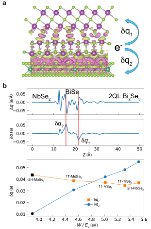
We examine the electronic properties of two interfaces in Bi2Se3/BiSe/TMDC and determine the amount of charge transfer. In Fig. 4a, we plot the isosurface of the electron density difference between the combined system and its individual components. One can clearly see that electron flows out of Bi orbitals in BiSe (yellow blobs) into Se orbitals in either TMDC or Bi2Se3 (pink blobs).
The plane-averaged electron density difference plot of the heterostructure is shown in Fig. 4b (top), where significant charge transfer occurs from the BiSe buffer layer (negative regions) to both NbSe2 and Bi2Se3 (positive regions). To quantify the amount of charge transfer at the two interfaces, we integrate the plane-averaged electron density difference along the surface normal direction to obtain the cumulative charge profile, as shown in Fig. 4b (bottom). Two pronounced peaks are indicated by the vertical red lines, corresponding to the net amount of charge transfer on each interface. The positive peak at the bottom interface corresponds to electron donation to NbSe2 with and the negative peak at the top interface corresponds to electron donation to Bi2Se3 with .
The trend of the charge transfer with respect to () is shown in Fig. 4c. As we expect, grows monotonously with (), varying from 0.01 to 0.06 . The smallest value of 0.01 is obtained on the 2H-MoSe2 substrate, with eV. On the other hand, overall shows a mild decay trend against (), except for 2H-NbSe2 which has a slightly larger (0.037 ) than 1T-TiSe2 (0.035 ). Since is primarily determined by the constant value of (1.68 eV), it exhibits a much narrower dynamic range from 0.035 to 0.044. Another factor that may contribute to the non-monotonic behavior of is the in-plane strain in the heterostructure, which will be discussed in Section III.5. There is more tensile strain in the Bi2Se3 and BiSe layers in Bi2Se3/BiSe/NbSe2 heterostructure than that in Bi2Se3/BiSe/TiSe2 (see Supplemental Material [52]), which may cause an enhancement of in the former and a reduction of in the latter.
III.4 Band structure and giant Rashba splitting
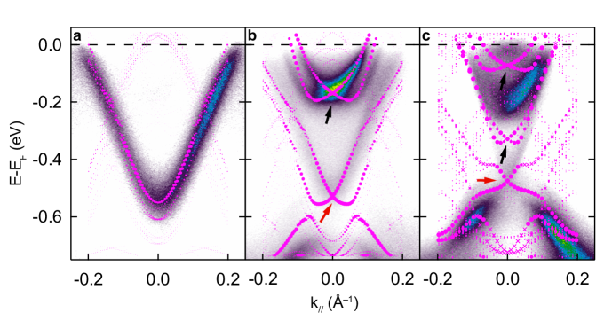
Recent ARPES measurements revealed interesting topological properties in few-layer Bi2Se3/BiSe/NbSe2 heterostructures [31]. To understand the ARPES data, the calculated band structures (pink dots) of the 1QL-, 2QL- and 3QL-Bi2Se3/BiSe/1ML-NbSe2 heterostructures are unfolded to the Brillouin zone of Bi2Se3 and overlaid on top of the measured band structure from Ref. [31] in Fig. 5. For this comparison, the calculated Fermi levels are slightly shifted by up to 0.15 eV to match the experiment. The amount of this adjustment is comparable to the differences in work function between DFT and experiment as shown in Table 2.
In the 1QL-Bi2Se3/BiSe/NbSe2 band structure (see Fig. 5a), ARPES shows a V-shape conduction band derived from Bi and Se orbitals of Bi2Se3, which is reproduced very well by our DFT calculations. The Bi2Se3 CBM is lower than the Fermi level by 0.55 eV, which is qualitatively reproduced by 0.70 eV from DFT. The valence band of Bi2Se3 is at lower energies outside the range of Fig. 5a.
In 2QL-Bi2Se3/BiSe/NbSe2, the surface states in Bi2Se3 are gapped, and the CBM shows a band splitting near the point indicated by the red arrow (see Fig. 5b). Due to the charge transfer between BiSe and Bi2Se3, the negative interface dipole along the out-of-plane direction breaks the inversion symmetry, which separates the DSSs in energy and weakens their coupling. DFT band structure qualitatively reproduces both the band gap and band splitting at the CBM, consistent with the schematic diagram in Fig. 1c. The underestimated gap and overestimated surface band splitting in DFT, as compared to experiment, are likely due to the limitation of the DFT method, which may not capture the screened long-range Coulomb repulsion between top and bottom surface states accurately [63].
Notably, we observe the giant Rashba band splitting in the quantum well (QW) state indicated by the black arrow, which is a strong evidence of the dipole-induced giant Rashba SOC effect. In contrast, the QW state in the Bi2Se3/NbSe2 band structure (i.e., without the BiSe buffer layer) resembles the pristine 2QL-Bi2Se3 with negligible Rashba splitting (see Fig. S2 in the Supplemental Material [52]). The Rashba constant is defined as , where and are energy and momentum splitting values. Based on the ARPES measurement, = 0.019 eV and = 0.038 Å-1, which yield = 1.0 eVÅ [31]. Values of , and from simulated band structures of 2QL-Bi2Se3/BiSe/NbSe2 heterostructures are listed in Table 4. In the heterostructure without strain, eVÅ is in excellent agreement with experiment. Note that the Au(111) surface, as a typical giant Rashba SOC material, has a Rashba constant of 0.33 eVÅ [64], and bulk BiTeI, among the highest Rashba SOC materials, has a Rashba constant of 3.8 eVÅ [65].
When the thickness of Bi2Se3 in the heterostructure increases to 3QLs, the Dirac point re-appears as indicated by the red arrow (see Fig. 5c), which is clearly reproduced by DFT. This feature is due to both the spatial separation of the top and bottom surface states and their energy offset caused by the interface dipole field. In fact, the interface electric field pulls the bottom surface state down into the bulk states, so the coupling between top and bottom surface states is weaker than the free-standing 3QL-Bi2Se3. In contrast, in pristine Bi2Se3 thin films the surface Dirac point appears only when the thickness is equal to or more than 6 QLs. In addition to the surface Dirac point, at higher energies, ARPES data also exhibit two QW states with giant Rashba band splitting. These QW states are reproduced by DFT calculations (indicated by black arrows), while the energy positions in DFT are closer to the Dirac point than the experiment by 0.09 eV, likely due to the limitation of the PBE functional. In Fig. 5c, we distinguish the quasiparticle states dominated by the bottom and top QLs with crosses and dots, respectively. The bottom-QL-dominated states do not appear in the experimental band structure, likely due to the thickness sensitivity of the ARPES measurement.
Overall, our calculations reproduce well all the key topological features in the ARPES measurement of few-layer Bi2Se3/BiSe/NbSe2 heterostructures, and the calculated giant Rashba constant is in excellent agreement with experiment.
In Table 4, we compare of different TMDC heterostructures based on the band splitting of the first QW state in 2QL-Bi2Se3/BiSe/TMDC. The calculated are between 1.0 eVÅ (1T-TiSe2) and 1.2 eVÅ (2H-MoSe2). Note that of the 2H-MoSe2 heterostructure is 9% larger than that of the 2H-NbSe2 heterostructure, which is consistent with the charge transfer analysis, as larger induces larger Rashba splitting.
| TMDCs | Exp888See Ref. [31] | |||||
| 2H-NbSe2 | 1H-TiSe2 | 1T-VSe2 | 1T-MoSe2 | 2H-MoSe2 | 2H-NbSe2 | |
| (eVÅ) | 1.1 | 1.0 | 1.1 | 1.1 | 1.2 | 1.0 |
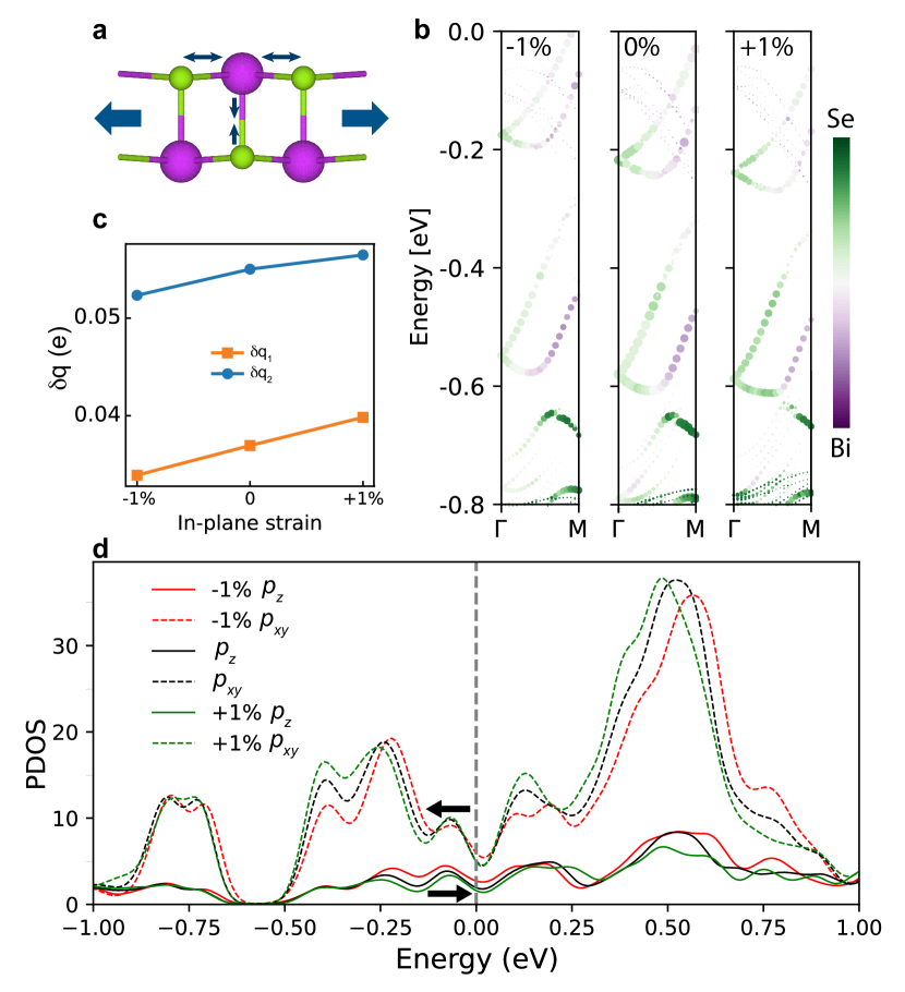
III.5 Effect of strain
The dipole field from the Bi2Se3/BiSe interface is the critical factor that leads to the novel topological properties in the Bi2Se3/BiSe/TMDC heterostructures. Therefore it is advantageous to have the ability to tune in order to enhance this dipole field, combined with a large enough to stabilize the BiSe buffer layer. As shown in Fig. 4c, the range of is about 0.0027 among the TMDCs (between 1T-MoSe2 that has a small work function and 2H-NbSe2 that has a large work function) that can grow the BiSe layer in experiment [29]. Here we consider strain as another means to control the interface charge transfer.
Strain can have significant effects on the electronic properties of 2D materials. Specifically, we investigate the effect of strain on the charge transfer at the two interfaces. We use the 2QL-Bi2Se3/BiSe/NbSe2 heterostructure as an exemplary system and apply a uniform in-plane strain between -1% and +1% to mimic the strain induced by the lattice mismatch between TMDCs and their substrate. We find that tensile strain enhances the charge transfer at the Bi2Se3/BiSe interface, while compressive strain suppresses it as shown in Fig. 6c. In fact, 1% tensile strain increases by 0.0029 , which is slightly larger than the effect (0.0027 ) caused by different TMDCs. As a result, heterostructures under tensile strain have larger Rashba splitting as shown in Fig. 6b. The calculated increases as a function of strain: , 1.1 and 1.4 eVÅ under 1% compressive strain, zero strain and 1% tensile strain, respectively. On the other hand, 1% tensile strain increases by 0.0015 , which is much smaller than the effects of different TMDCs (0.024 ).
To understand the effects of strain on charge transfer, we focus on the BiSe buffer layer and plot the PDOS of BiSe in Fig. 6d. The in-plane tensile strain effectively stretches the in-plane Bi-Se bond and compresses the out-of-plane Bi-Se bond in the BiSe monolayer as shown in Fig. 6a. Consequently, the / anti-bonding orbitals move to lower energy and anti-bonding orbitals move to higher energy, indicated by black arrows. Thus, the electrons in BiSe become more unstable than those without strain, which enhances the charge transfer of Bi electrons to neighboring layers in both upper and lower interfaces.
IV CONCLUSION
In this work, we systematically study a series of Bi2Se3/BiSe/TMDC heterostructures with small lattice mismatch using first-principles calculations. With detailed analysis of the band alignment and charge transfer, we show that the rock-salt BiSe buffer layer can donate electrons to both Bi2Se3 and TMDC layers and the magnitude depends on the work function (or electron affinity) difference. We show that TMDCs with a large work function is more favorable to stabilize the BiSe buffer layer and cause a larger amount of charge transfer on the BiSe/TMDC interface, but with a much weaker impact on the charge transfer at the Bi2Se3/BiSe interface.
The resulting dipole at the Bi2Se3/BiSe interface creates an out-of-plane electric field that breaks the inversion symmetry in the Bi2Se3 layer and introduces an energy offset to the top and bottom Dirac surface states. As a result, new topological properties emerge in few-QL Bi2Se3, including giant Rahsba band splitting in the quantum well states in 2QL-Bi2Se3/BiSe/NbSe2 and the re-appearance of the Dirac point in 3QL-Bi2Se3/BiSe/NbSe2. These results are in excellent agreement with the experimental band structure in the literature from ARPES measurements. In addition, we find that tensile strain can significantly enhance the charge transfer on both interfaces from the BiSe anti-bonding orbitals, which provides another mechanism to control the topological properties of Bi2Se3/BiSe/TMDC heterostructures.
The emergence of Dirac surface states in quasi-2D materials may open a new avenue for new quantum material platforms, which require the interplay of topological states with strong proximity effects of superconductivity or charge density wave phase.
Acknowledgements.
We thank Dr. Cui-Zu Chang for providing the ARPES data used in this study. This research used resources from the Center for Functional Nanomaterials (CFN), which is a U.S. Department of Energy Office of Science User Facility, at Brookhaven National Laboratory under Contract No. DE-SC0012704. This research also used resources of the National Synchrotron Light Source II, a US Department of energy (DOE) Office of Science User Facility operated for the DOE Office of Science by Brookhaven National Laboratory under Contract number DE-SC0012704.References
- Hasan and Kane [2010] M. Z. Hasan and C. L. Kane, Colloquium: topological insulators, Reviews of modern physics 82, 3045 (2010).
- Shen [2012] S.-Q. Shen, Topological insulators, Vol. 174 (Springer, 2012).
- Moore [2010] J. E. Moore, The birth of topological insulators, Nature 464, 194 (2010).
- Fu et al. [2007] L. Fu, C. L. Kane, and E. J. Mele, Topological insulators in three dimensions, Physical review letters 98, 106803 (2007).
- Fan and Wang [2016] Y. Fan and K. L. Wang, Spintronics based on topological insulators, in Spin, Vol. 6 (World Scientific, 2016) p. 1640001.
- He et al. [2019] M. He, H. Sun, and Q. L. He, Topological insulator: Spintronics and quantum computations, Frontiers of Physics 14, 1 (2019).
- Plank et al. [2016] H. Plank, S. N. Danilov, V. V. Bel’kov, V. A. Shalygin, J. Kampmeier, M. Lanius, G. Mussler, D. Grützmacher, and S. D. Ganichev, Opto-electronic characterization of three dimensional topological insulators, Journal of Applied Physics 120 (2016).
- Politano et al. [2017] A. Politano, L. Viti, and M. S. Vitiello, Optoelectronic devices, plasmonics, and photonics with topological insulators, APL Materials 5 (2017).
- Xu et al. [2017] N. Xu, Y. Xu, and J. Zhu, Topological insulators for thermoelectrics, npj Quantum Materials 2, 51 (2017).
- Müchler et al. [2013] L. Müchler, F. Casper, B. Yan, S. Chadov, and C. Felser, Topological insulators and thermoelectric materials (2013).
- Qi and Zhang [2011] X.-L. Qi and S.-C. Zhang, Topological insulators and superconductors, Reviews of Modern Physics 83, 1057 (2011).
- Fu and Kane [2008] L. Fu and C. L. Kane, Superconducting proximity effect and majorana fermions at the surface of a topological insulator, Physical review letters 100, 096407 (2008).
- Pan et al. [2022] H. Pan, M. Xie, F. Wu, and S. D. Sarma, Topological phases in ab-stacked mote 2/wse 2: Z 2 topological insulators, chern insulators, and topological charge density waves, Physical Review Letters 129, 056804 (2022).
- Mitsuishi et al. [2020] N. Mitsuishi, Y. Sugita, M. Bahramy, M. Kamitani, T. Sonobe, M. Sakano, T. Shimojima, H. Takahashi, H. Sakai, K. Horiba, et al., Switching of band inversion and topological surface states by charge density wave, Nature communications 11, 2466 (2020).
- Hor et al. [2010] Y. Hor, P. Roushan, H. Beidenkopf, J. Seo, D. Qu, J. Checkelsky, L. Wray, D. Hsieh, Y. Xia, S.-Y. Xu, et al., Development of ferromagnetism in the doped topological insulator bi 2- x mn x te 3, Physical Review B 81, 195203 (2010).
- Wang et al. [2016] H. Wang, J. Kally, J. S. Lee, T. Liu, H. Chang, D. R. Hickey, K. A. Mkhoyan, M. Wu, A. Richardella, and N. Samarth, Surface-state-dominated spin-charge current conversion in topological-insulator–ferromagnetic-insulator heterostructures, Physical review letters 117, 076601 (2016).
- Thiel et al. [2006] S. Thiel, G. Hammerl, A. Schmehl, C. W. Schneider, and J. Mannhart, Tunable quasi-two-dimensional electron gases in oxide heterostructures, Science 313, 1942 (2006).
- He et al. [2016] Y. He, Y. Yang, Z. Zhang, Y. Gong, W. Zhou, Z. Hu, G. Ye, X. Zhang, E. Bianco, S. Lei, et al., Strain-induced electronic structure changes in stacked van der waals heterostructures, Nano letters 16, 3314 (2016).
- Lin et al. [2016] Z. Lin, A. McCreary, N. Briggs, S. Subramanian, K. Zhang, Y. Sun, X. Li, N. J. Borys, H. Yuan, S. K. Fullerton-Shirey, et al., 2d materials advances: from large scale synthesis and controlled heterostructures to improved characterization techniques, defects and applications, 2D Materials 3, 042001 (2016).
- Zhang et al. [2010a] Y. Zhang, K. He, C.-Z. Chang, C.-L. Song, L.-L. Wang, X. Chen, J.-F. Jia, Z. Fang, X. Dai, W.-Y. Shan, et al., Crossover of the three-dimensional topological insulator bi2se3 to the two-dimensional limit, Nature Physics 6, 584 (2010a).
- Zhang et al. [2009] H. Zhang, C.-X. Liu, X.-L. Qi, X. Dai, Z. Fang, and S.-C. Zhang, Topological insulators in bi2se3, bi2te3 and sb2te3 with a single dirac cone on the surface, Nature physics 5, 438 (2009).
- Zhang et al. [2010b] W. Zhang, R. Yu, H.-J. Zhang, X. Dai, and Z. Fang, First-principles studies of the three-dimensional strong topological insulators bi2te3, bi2se3 and sb2te3, New Journal of Physics 12, 065013 (2010b).
- Mazumder and Shirage [2021] K. Mazumder and P. M. Shirage, A brief review of bi2se3 based topological insulator: from fundamentals to applications, Journal of Alloys and Compounds 888, 161492 (2021).
- Manzeli et al. [2017] S. Manzeli, D. Ovchinnikov, D. Pasquier, O. V. Yazyev, and A. Kis, 2d transition metal dichalcogenides, Nature Reviews Materials 2, 1 (2017).
- Choi et al. [2017] W. Choi, N. Choudhary, G. H. Han, J. Park, D. Akinwande, and Y. H. Lee, Recent development of two-dimensional transition metal dichalcogenides and their applications, Materials Today 20, 116 (2017).
- Wang et al. [2017] H. Wang, X. Huang, J. Lin, J. Cui, Y. Chen, C. Zhu, F. Liu, Q. Zeng, J. Zhou, P. Yu, et al., High-quality monolayer superconductor nbse2 grown by chemical vapour deposition, Nature communications 8, 394 (2017).
- Goli et al. [2012] P. Goli, J. Khan, D. Wickramaratne, R. K. Lake, and A. A. Balandin, Charge density waves in exfoliated films of van der waals materials: evolution of raman spectrum in tise2, Nano letters 12, 5941 (2012).
- Yilmaz et al. [2023] T. Yilmaz, X. Jiang, D. Lu, P. M. Sheverdyaeva, A. V. Matetskiy, P. Moras, F. Mazzola, I. Vobornik, J. Fujii, K. Evans-Lutterodt, et al., Dirac nodal arc in 1t-vse2, Communications Materials 4, 47 (2023).
- Choffel et al. [2021a] M. A. Choffel, R. N. Gannon, F. Göhler, A. M. Miller, D. L. Medlin, T. Seyller, and D. C. Johnson, Synthesis and electrical properties of a new compound (bise) 0.97 (bi2se3) 1.26 (bise) 0.97 (mose2) containing metallic 1t-mose2, Chemistry of Materials 33, 6403 (2021a).
- Choffel et al. [2021b] M. A. Choffel, T. M. Kam, and D. C. Johnson, Substituent effects in the synthesis of heterostructures, Inorganic Chemistry 60, 9598 (2021b).
- Yi et al. [2022] H. Yi, L.-H. Hu, Y. Wang, R. Xiao, J. Cai, D. R. Hickey, C. Dong, Y.-F. Zhao, L.-J. Zhou, R. Zhang, et al., Crossover from ising-to rashba-type superconductivity in epitaxial bi2se3/monolayer nbse2 heterostructures, Nature Materials 21, 1366 (2022).
- Kamminga et al. [2020] M. E. Kamminga, M. Batuk, J. Hadermann, and S. J. Clarke, Misfit phase (bise) 1.10 nbse2 as the origin of superconductivity in niobium-doped bismuth selenide, Communications Materials 1, 82 (2020).
- Mitchson et al. [2015] G. Mitchson, M. Falmbigl, J. Ditto, and D. C. Johnson, Antiphase boundaries in the turbostratically disordered misfit compound (bise) 1+ nbse2, Inorganic Chemistry 54, 10309 (2015).
- Petříček et al. [1993] V. Petříček, I. Cisarova, J. De Boer, W. Zhou, A. Meetsma, G. Wiegers, and S. Van Smaalen, The modulated structure of the commensurate misfit-layer compound (bise) 1.09 tase2, Acta Crystallographica Section B: Structural Science 49, 258 (1993).
- Trump et al. [2014] B. A. Trump, K. J. Livi, and T. M. McQueen, The new misfit compound (bise) 1.15 (tise2) 2 and the role of dimensionality in the cux (bise) 1+ (tise2) n series, Journal of Solid State Chemistry 209, 6 (2014).
- Nader et al. [1997] A. Nader, A. Briggs, and Y. Gotoh, Superconductivity in the misfit layer compounds (bise) 1.10 (nbse2) and (bis) 1.11 (nbs2), Solid state communications 101, 149 (1997).
- Smeller et al. [2012] M. M. Smeller, C. L. Heideman, Q. Lin, M. Beekman, M. D. Anderson, P. Zschack, I. M. Anderson, and D. C. Johnson, Structure of turbostratically disordered misfit layer compounds [(pbse) 0.99] 1 [wse2] 1,[(pbse) 1.00] 1 [mose2] 1, and [(snse) 1.03] 1 [mose2] 1, Zeitschrift für anorganische und allgemeine Chemie 638, 2632 (2012).
- Giang et al. [2010] N. Giang, Q. Xu, Y. Hor, A. Williams, S. Dutton, H. Zandbergen, and R. Cava, Superconductivity at 2.3 k in the misfit compound (pbse) 1.16 (tise 2) 2, Physical Review B 82, 024503 (2010).
- Lin et al. [2010] Q. Lin, M. Smeller, C. L. Heideman, P. Zschack, M. Koyano, M. D. Anderson, R. Kykyneshi, D. A. Keszler, I. M. Anderson, and D. C. Johnson, Rational synthesis and characterization of a new family of low thermal conductivity misfit layer compounds [(pbse) 0.99] m (wse2) n, Chemistry of Materials 22, 1002 (2010).
- Chikina et al. [2022] A. Chikina, G. Bhattacharyya, D. Curcio, C. E. Sanders, M. Bianchi, N. Lanatà, M. Watson, C. Cacho, M. Bremholm, and P. Hofmann, One-dimensional electronic states in a natural misfit structure, Physical Review Materials 6, L092001 (2022).
- Yao et al. [2018] Q. Yao, D. Shen, C. Wen, C. Hua, L. Zhang, N. Wang, X. Niu, Q. Chen, P. Dudin, Y. Lu, et al., Charge transfer effects in naturally occurring van der waals heterostructures (pbse) 1.16 (tise 2) m (m= 1, 2), Physical Review Letters 120, 106401 (2018).
- Song et al. [2022] Z. Song, J. Huang, S. Zhang, Y. Cao, C. Liu, R. Zhang, Q. Zheng, L. Cao, L. Huang, J. Wang, et al., Observation of an incommensurate charge density wave in monolayer tise 2/cuse/cu (1 1 1) heterostructure, Physical Review Letters 128, 026401 (2022).
- Esters et al. [2018] M. Esters, R. G. Hennig, and D. C. Johnson, Insights into the charge-transfer stabilization of heterostructure components with unstable bulk analogs, Chemistry of Materials 30, 4738 (2018).
- Wang et al. [2014] M.-X. Wang, P. Li, J.-P. Xu, Z.-L. Liu, J.-F. Ge, G.-Y. Wang, X. Yang, Z.-A. Xu, S.-H. Ji, C. Gao, et al., Interface structure of a topological insulator/superconductor heterostructure, New Journal of Physics 16, 123043 (2014).
- Mitchson et al. [2016] G. Mitchson, E. Hadland, F. Göhler, M. Wanke, M. Esters, J. Ditto, E. Bigwood, K. Ta, R. G. Hennig, T. Seyller, et al., Structural changes in 2d bise bilayers as n increases in (bise) 1+ (nbse2) n (n= 1–4) heterostructures, ACS nano 10, 9489 (2016).
- Kresse and Joubert [1999] G. Kresse and D. Joubert, From ultrasoft pseudopotentials to the projector augmented-wave method, Physical review b 59, 1758 (1999).
- Kresse and Hafner [1993] G. Kresse and J. Hafner, Ab initio molecular dynamics for liquid metals, Physical review B 47, 558 (1993).
- Kresse and Furthmüller [1996a] G. Kresse and J. Furthmüller, Efficiency of ab-initio total energy calculations for metals and semiconductors using a plane-wave basis set, Computational materials science 6, 15 (1996a).
- Kresse and Furthmüller [1996b] G. Kresse and J. Furthmüller, Efficient iterative schemes for ab initio total-energy calculations using a plane-wave basis set, Physical review B 54, 11169 (1996b).
- Perdew et al. [1996] J. P. Perdew, K. Burke, and M. Ernzerhof, Generalized gradient approximation made simple, Physical review letters 77, 3865 (1996).
- Grimme [2006] S. Grimme, Semiempirical gga-type density functional constructed with a long-range dispersion correction, Journal of computational chemistry 27, 1787 (2006).
- [52] See supplemental material at, {https://URLwillbeinsertedbypublisher}.
- Bengtsson [1999] L. Bengtsson, Dipole correction for surface supercell calculations, Physical Review B 59, 12301 (1999).
- Wang et al. [2021] V. Wang, N. Xu, J.-C. Liu, G. Tang, and W.-T. Geng, Vaspkit: A user-friendly interface facilitating high-throughput computing and analysis using vasp code, Computer Physics Communications 267, 108033 (2021).
- [55] Q. Zheng, Vasp band unfolding, https://github.com/QijingZheng/VaspBandUnfolding.
- Tang et al. [2009] W. Tang, E. Sanville, and G. Henkelman, A grid-based bader analysis algorithm without lattice bias, Journal of Physics: Condensed Matter 21, 084204 (2009).
- Ni et al. [2022] X. Ni, H. Li, and J.-L. Brédas, Organic self-assembled monolayers on superconducting nbse2: interfacial electronic structure and energetics, Journal of Physics: Condensed Matter 34, 294003 (2022).
- Liu et al. [2016] Y. Liu, P. Stradins, and S.-H. Wei, Van der waals metal-semiconductor junction: Weak fermi level pinning enables effective tuning of schottky barrier, Science advances 2, e1600069 (2016).
- Kim and Choi [2021] H.-g. Kim and H. J. Choi, Thickness dependence of work function, ionization energy, and electron affinity of mo and w dichalcogenides from dft and gw calculations, Physical Review B 103, 085404 (2021).
- Wong et al. [2019] P. K. J. Wong, W. Zhang, F. Bussolotti, X. Yin, T. S. Herng, L. Zhang, Y. L. Huang, G. Vinai, S. Krishnamurthi, D. W. Bukhvalov, et al., Evidence of spin frustration in a vanadium diselenide monolayer magnet, Advanced materials 31, 1901185 (2019).
- Liu et al. [2018] Z.-L. Liu, X. Wu, Y. Shao, J. Qi, Y. Cao, L. Huang, C. Liu, J.-O. Wang, Q. Zheng, Z.-L. Zhu, et al., Epitaxially grown monolayer vse2: an air-stable magnetic two-dimensional material with low work function at edges, Science bulletin 63, 419 (2018).
- Zhang et al. [2019] Q. Zhang, S. Zhang, B. A. Sperling, and N. V. Nguyen, Band offset and electron affinity of monolayer mose 2 by internal photoemission, Journal of Electronic Materials 48, 6446 (2019).
- Liu et al. [2023] J.-n. Liu, X. Yang, H. Xue, X.-s. Gai, R. Sun, Y. Li, Z.-Z. Gong, N. Li, Z.-K. Xie, W. He, et al., Surface coupling in bi2se3 ultrathin films by screened coulomb interaction, Nature Communications 14, 4424 (2023).
- LaShell et al. [1996] S. LaShell, B. McDougall, and E. Jensen, Spin splitting of an au (111) surface state band observed with angle resolved photoelectron spectroscopy, Physical review letters 77, 3419 (1996).
- Ishizaka et al. [2011] K. Ishizaka, M. Bahramy, H. Murakawa, M. Sakano, T. Shimojima, T. Sonobe, K. Koizumi, S. Shin, H. Miyahara, A. Kimura, et al., Giant rashba-type spin splitting in bulk bitei, Nature materials 10, 521 (2011).