- GFET
- graphene field effect transistor
- FET
- field effect transistor
- cQD
- colloidal quantum dot
- AFM
- atomic force microscope
- L
- channel length
- W
- channel width
- EHD
- electrohydrodynamic nanoprinting
- IR
- infrared
- SWIR
- short wave infrared
- PSD
- power spectral density
- EDT
- ethane-1,2-dithiol
- LbL
- layer-by-layer
- NEI
- noise equivalent irradiance
- NEP
- noise equivalent power
- LSQ
- least squares fit
- TLM
- transfer length method
Scaling of Hybrid QDs-Graphene Photodetectors to Subwavelength Dimension
Gökhan Karaa, Patrik Rohnera,b, Erfu Wua, Dmitry N. Dirinb,d, Roman Furrera, Dimos Poulikakosc, Maksym V. Kovalenkob,d, Michel Calamea,e, Ivan Shorubalkoa,*
(a) Laboratory for Transport at Nanoscale Interfaces, Empa – Swiss Federal Laboratories for Materials Science and Technology, CH-8600 Dübendorf, Switzerland
(b) Department of Chemistry and Applied Biosciences, ETH – Swiss Federal Institute of Technology Zurich, CH-8093 Zurich, Switzerland
(c) Laboratory of Thermodynamics in Emerging Technolohgies, Department of Mechanical and Process Engineering, ETH – Swiss Federal Institute of Technology Zurich, CH-8092 Zurich, Switzerland
(d) Laboratory for Thin Films and Photovoltaics, Empa – Swiss Federal Laboratories for Materials Science and Technology, CH-8600 Dübendorf, Switzerland
(e) Department of Physics and Swiss Nanoscience Institute, University of Basel , CH-4056 Basel, Switzerland
* Email: ivan.shorubalko@empa.ch
Abstract
Emerging colloidal quantum dot (cQD) photodetectors currently challenge established state-of-the-art infrared photodetectors in response speed, spectral tunability, simplicity of solution processable fabrication, and integration onto curved or flexible substrates. Hybrid phototransistors based on 2D materials and cQDs, in particular, are promising due to their inherent photogain enabling direct photosignal enhancement. The photogain is sensitive to both, measurement conditions and photodetector geometry. This makes the cross-comparison of devices reported in the literature rather involved. Here, the effect of device length and width scaling to subwavelength dimensions (sizes down to \qty500nm) on the photoresponse of graphene-PbS cQD phototransistors was experimentally investigated. Photogain and responsivity were found to scale with , whereas the photocurrent and specific detectivity were independent of geometrical parameters. The measurements were performed at scaled bias voltage conditions for comparable currents. Contact effects were found to limit the photoresponse for devices with \unit. The relation of gate voltage, bias current, light intensity, and frequency on the photoresponse was investigated in detail, and a photogating efficiency to assess the cQD-graphene interface is presented. In particular, the specific detectivity values in the range between to \unitJones (wavelength of \qty1550nm, frequency \qty6Hz, room temperature) were found to be limited by the charge transfer across the photoactive interface.
Keywords: colloidal quantum dots, graphene, phototransistors, infrared photodetectors, scaling, subwavelength
Introduction
Emerging photodetectors based on colloidal quantum dots (cQDs) are currently challenging state-of-the-art infrared (IR) photodectors by low cost solution processing1, 2, simple spectral tunability1, 2, multiband absorption3, 4, 5, response speed6, 7, 8, and integration onto flexible substrates9, 10, 11, 12. PbS cQDs SWIR photodiode arrays were recently fabricated with a pixel pitch of \qty1.62.13 This is about five times smaller than the pixel size of common InGaAs photodetectors. Reduced dimension are, on the contrary, also limiting the number of photons reaching a detector. The integration of photonic structures is, thus, an attractive way to enhance light-matter interaction in cQD photodetectors.14, 15 Another way to overcome low light levels is by coupling a light absorber with a transistor. By introducing PbS cQDs as a photogate to a graphene field effect transistor (GFET), photoresponsivities of to \unitA \perW were demonstrated.16, 17 The high responsivity values were also reflected in the specific detectivity of \unitJones at room temperature16 that is comparable to commercial InGaAs photodetectors.
Research in hybrid phototransistors is focused on reducing dark currents by exchanging the transistor channel material with TMDCs18, 19, 20, 21 or metal oxides22, 12, energy barrier engineering19, 9, 23, 24, longer charge extraction distance in the cQD films25, extending the spectral range to longer wavelength 26, 27, 21, or technological applicability to flexible substrates9, 11, 12 and printing28, 26, 29. Although it is commonly reported that the photogain follows a dependence in those devices30, 31, 32, limited effort has been spent to experimentally validate this prediction. In addition, the photoresponse is highly dependent on measurement conditions (e.g., bias, illumination), geometry, and batch-specific fabrication. Thus, reproducibility and the cross-comparison of individual reports remain highly involved, and derived scaling laws are inconclusive.
Here, we experimentally demonstrate the scaling of hybrid graphene - PbS cQD phototransistors with channel length, width, and cQD film thickness. We highlight a dependence of the photogain and responsivity, and a dimension-independent photocurrent and specific detectivity at scaled bias voltage condition for comparable currents. We further show the photoresponse’s gate voltage, bias current, light intensity, and frequency dependency and derive a photogating efficiency for a cQD-graphene interface evaluation.
Results and Discussion
Photocurrent Relation of Hybrid Phototransistors
Figure 1 (a) shows a cross-section of a hybrid phototransistor. Two gold electrodes (source and drain) contact the graphene channel, and a p-Si back gate enables charge carrier density tuning in the channel by the field effect. The phototransistor has a channel length (L), width (W), and a cQDs film thickness as the photogate on top. The incoming light creates electron-hole (e-h) pairs in the absorbing cQD layer. The Fermi level alignment between graphene and the cQD film causes an electric field at the interface (depletion region) that separates the photo-generated e-h pairs and leads to the commonly observed hole transfer to the graphene channel. The electrons stay trapped in the film for a time , gating the channel.16 The photoinitiated e-h separation current between the cQDs film and graphene is small compared to the channel current and is thus neglected. The photogate modulation of is an enhancement of the photosignal and is described as photogain by the rate equation
| (1) |
is the transit time of a charge carrier in the channel between source and drain contacts.30, 33, 32 Within the Drude model, the transit time can be stated by bias condition and geometry of the channel and leads to
| (2) |
is the bias voltage between source and drain, and the charge carrier mobility in the channel. The photocurrent of the hybrid phototransistors can thus be described by
| (3) |
where the elementary charge, and is a photogating efficiency describing how likely an incoming photon is creating a charge photogating the transistor channel.34, 30 The photonflux is defined by the incoming light power and photon energy . is Planck’s constant, the speed of light, and the wavelength of the incoming light. Thus, the photoresponsivity
| (4) |
is proportional to the and often stated as .
Figure 1 (a) also shows the experimental setup used to characterize the photoresponse of the investigated detectors. A bias voltage was applied between the source and drain contacts, and the current was measured simultaneously. A gate voltage was applied to the back gate to control the 2D charge carrier density in the graphene channel, where \unitnF\percm^2 is the capacitance of the gate oxide. The incoming light was chopped at a frequency . This light modulation induced an AC photocurrent on top of that was extracted as a voltage drop over a shunt resistance. The incoming light power was characterized by a reference detector. The calculated the photoresponsivity for a sub-wavelength dimensioned device of \unit^2 is shown in Figure 1 (b). The inset shows the AFM image of the characterized device before cQD sensitization. A photoresponsivity of \qty150A\perW was reached at the first excitonic peak at \qty1530nm. The spin-coating of the PbS cQDs lead to a blue shift of about \qty70nm compared to their excitonic peak at \qty1600nm (diameter \qty6nm)35 after synthesis. All measurements were performed in vacuum and at room temperature.
Further, electrohydrodynamic nanoprinting (EHD) and layer-by-layer (LbL) spin coating were compared to assess the influence of cQD deposition techniques on the photoresponse. First, in Figure 1 (c), the deposition of cQDs by EHD printing is depicted. By applying an AC voltage between the gold coated nozzle and the substrate, cQDs accumulate at the formed meniscus, and droplets markedly smaller than the nozzle diameter are pulled out by the electric field from the apex of the meniscus. This enables printing features with a resolution in the \qty100nm range.36, 37 For PbS cQDs in particular, a resolution of \qty1 was previously demonstrated.28 This method enables precise spatial control of placing cQDs in a desired geometrical pattern. After printing, a solid-state ligand exchange treatment was performed to substitute the native oleic acid with ethane-1,2-dithiol ligands. This single-step treatment reduces the interparticle distance, a shrinkage of about 40% was observed, leading to conductive films. Additionally, the extra control of film thickness by EHD printing on a single sample level allowed to vary between 65 to \qty120nm. The geometry of the device channels were \unit^2.
The second applied method was the layer-by-layer (LbL) spin coating. A thin layer of cQDs was spin coated and directly treated with a solid-state ligand exchange procedure to EDT. These two steps were repeated six times, resulting in of \qty170nm. By this method, devices with different ranging from 20 down to 0.5 \unit and a \unit were sensitized with cQDs. In addition, the scaling was investigated by changing the width between 5 down to 0.5 \unit with a fixed \unit. Figure 1 (d) shows the investigated devices with the LbL spin-coating approach before deposition. In contrast to printing, the entire sample was covered with one cQD thickness (inset). The LbL spin coating has been proven to yield dense and crack-free conductive films38, optimally suited for solar cells and photodetectors.39, 40, 41
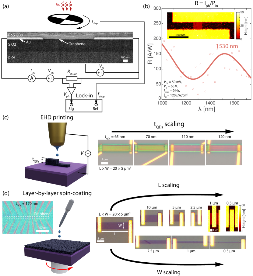
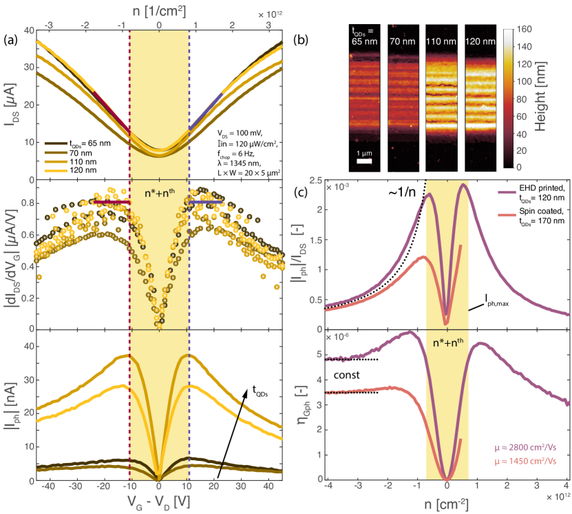
Figure 2 (a) shows the characterized devices of EHD-printed cQDs films with different layer thicknesses. From top to down, the plots show the source-drain currents , transconductance and the amplitude of the photocurrent while the gate voltage was swept. was derived by a numerical derivative from . The measurements were performed at a bias voltage of \qty100mV, irradiance of \qty120\microW \percm^2, chopping frequency of \qty6Hz, and the curves were corrected by the individual Dirac point voltage (charge neutrality point) of the GFETs (average of \qty-20V). The first excitonic peak of the cQDs shifted to a wavelength of \qty1345nm (shift of about 250 nm). The blue shift of the absorption peak might be explained by oxidation of the cQDs during printing. The maximum of the measured photocurrent was found at the left, hole-doped region , and right, electron-doped region , of the Dirac point. The dashed lines (red and blue) indicate where the maximum photocurrents were measured that, on average, corresponds to 10 V ( \unit1/cm^2) from the Dirac point.
The solid red and blue lines (p- and n-doped region) in the and plots indicate where reaches about a constant maximum, as illustrated for the device with \unitnm. The maxima of the photocurrent coincide with this region and thus are found where the transconductance is the highest, as reported previously.42 The yellow shaded region of Figure 2 (a) indicates the influenced region by random potential fluctuations around the Dirac point in graphene. In this region, the applied gate voltage loses its ability to tune up to a point where charges are only redistributed locally (e-h charge puddles) and, thus, does not affect the conductivity anymore. This causes a drop of towards the Dirac point and depends on residual doping and temperature .43
Figure 2 (b) depicts the four devices’ AFM images after ligand exchange treatment. Thicker cQD films absorb more light reaching 100% absorption at about \qty500nm for an absorption coefficient of \unit\percm.35 Correspondingly, an increasing trend of the photocurrent with thicker films is observed in the bottom panel of Figure 2 (a). However, to extract charges from the cQD layer, they need to be in the depletion region close to the interface.25 This is why a saturation of the photocurrent is expected before \unitnm is reached. In a previous study, this saturation thickness was found to be about \qty160nm for EHD-printed cQD films.28
The photoresponsivity is used to assess detectors’ efficiency in converting light into a photocurrent. However, is a derived quantity and describes the proportionality between the photocurrent and the incoming light power.34 Thus, in this study, the main focus was put on as the measured quantity at compatable conditions across the investigated devices. Also, applying a constant bias voltage might not always be applicable over the different length scales as the current is proportionally increasing with . A comparison should thus aim to keep the applied electric field constant, which induces a constant condition. Therefore, equation (2) can be reexpressed with a bias-current, and further taking the channel conductivity () into account, yields
| (5) |
Likewise, devices observe the same irradiance rather than the same light power . Including (5) and into equation (3) hence results in
| (6) |
and predicts a geometry-independent photocurrent. Note that states the charge carrier density for electrons if positive and for holes if negative to account for the ambipolar graphene FET behavior.
In Figure 2 (c), the photocurrent of two devices close to the photocurrent saturation limited film thickness were compared. The two devices were fabricated independently, and the cQDs deposition method was varied between EHD printing and LbL spin coating as described in Figure 1 (b) and (c). was normalized by to account for contact resistances. The photoresponse shows a proportionality, and drops to zero at the Dirac point of graphene.
Although solid-state ligand exchanged cQD films are predominantly fabricated by a LbL approach in the literature, they do not necessarily result in a higher conductivity than a single-step ligand exchanged approach.38 Accordingly, the devices with the EHD printed cQD films (single-step ligand exchange) demonstrate a slightly higher photoresponse of about a factor of 1.8. The ratio of the mobilities is about 1.9. Using equation (6), the photogating efficiency was estimated from the experiments as shown in the bottom panel. The extracted also takes the different wavelengths from the measurements (different first excitonic peaks, although the same cQD are used for the different devices) into account. The efficiency ratio is about 1.6 and similar to the and ratios. The photogating efficiency can further be expressed as
| (7) |
where describes the charge transfer efficiency, how well a photogenerated charge can be extracted from the cQD layer to graphene, and light absorption efficiency, how many e-h pairs are generated per incident photon.30, 33, 44 Furthermore, can be estimated to be in the range of 0.6 to 0.8. As the magnitude of is in the order of and one order of magnitude is lost to the absorption (), there is only about one every charge carriers that are extracted to graphene. Thus is a major source for improvement and stresses that a single-step ligand exchange is not a limiting factor.
Scaling of Pixel Dimensions
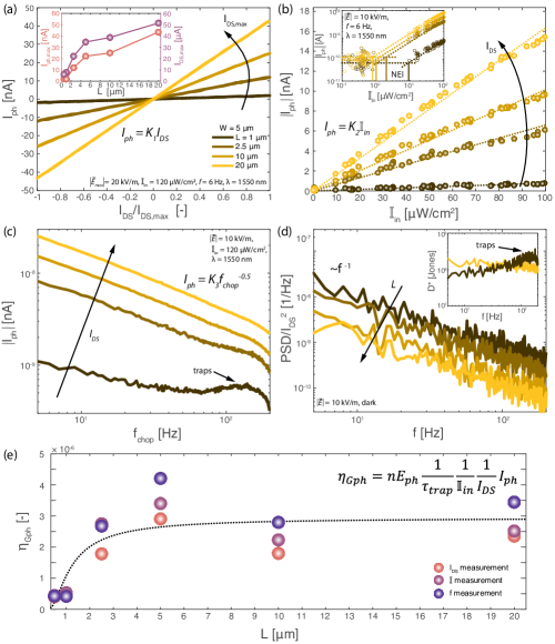
Next, the geometrical scaling of hybrid graphene – cQD phototransistors was investigated. All devices were fabricated on the same sample, and the cQD film was prepared by LbL spin coating to reduce device-to-device variations. First, equation (6) was validated by bias, irradiance, and frequency sweeps for devices with different and a of \qty5. Figure 3 (a) shows the linear relation between the source-drain current and with a proportionality factor . The bias voltage was scaled according to for comparable electric fields in the different devices. For better visualization, the measured source-drain current was normalized by its highest value . The inset shows each device’s highest photocurrents at . Every device was measured at the gate voltage where the highest photocurrent was observed in the p-doped region of graphene (red dashed line in Figure 2 (b)). The n-doped photocurrent maxima was experimentally not accessible as the LbL spin coating led to Dirac point voltages up to \qty70V.
From equation (6), there is no length dependence expected, and all curves in Figure 3 (a) should lay on a single line. The inset shows that despite the applied comparable electric field condition across devices, still scales with . This can be explained by a voltage drop over the contacts that becomes comparable to the voltage drop over the channel for smaller , and thus is not the same over the different channels despite the scaled . The contact resistance is estimated to be in the range of about \qty0.6kΩ per contact by performed transfer length method (TLM) measurements. Thus, the ratio of and the channel resistance become comparable () for devices with \unit. Reversibly, the contact resistance can be estimated from the spread of the vs. curves assuming the same over the channel leads to the same . This also results in \unitkΩ. With the fact that is linearly proportional to , this confirms the origin of the spread from contact limitations.
In Figure 3 (b), irradiance sweeps were performed for the same set of devices. This – relation is linear with a proportionality factor . is related to the responsivity by . As the curves follow a linear fit (dotted line), the detectors were operated in the linear dynamic regime (), reaching responsivity values about \qty300A\perW for \unitkV/m and \unitHz. The inset highlights the noise equivalent irradiance (NEI) for the different devices in the range of 1 to \qty10μW\percm^2. The specific detectivity can be calculated by32, 30
| (8) |
is the noise equivalent power, the frequency bandwidth, and the noise current. The resulting detectivities are about \unitJones at \qty6Hz and with \unitHz (equivalent noise bandwidth of lock-in measurement).
Figure 3 (c) shows the frequency response of the investigated devices. The light chopping frequency was varied between 5 and \qty200Hz. A fit to data relates dependence, where is a proportionality constant. The curves follow ( 0.1) up to frequencies of about \qty160Hz. A differing photocurrent dynamics can be observed for the \qty1 channel length device (dark brown). Around \qty70Hz, the trend deviates from the as increases with before it drops eventually.
The chopping frequency is defined over which period the detector sees the light. Thus, it probes of the cQD film. Previous experiments have shown that at least two trapping times can be present underlying the photocurrent dynamics.45, 29, 46 In analogy to low frequency noise47, the frequency response might originate from an envelope of individual Lorentzian shaped trap state contributions. Thus, the slope of the envelope is a cQD film-dependent quantity and depends on the specific film treatment as it varies across the literature (values between -0.1 to -2).25, 11, 45 Within this frame, a possible explanation of the rise of around \qty130Hz might be the quenched escape rate from such a trap, as new carriers are excited before the trapped ones escape. Consequently, the traps might be constantly populated, and newly photoexcited e-h pairs can escape without being slowed down from those traps, leading to higher photocurrents. The energy depth of such a trap can be estimated by , with the Boltzmann constant, and the temperature.48 The free charge carrier lifetime is the recombination time of a charge carrier contributing to the photocurrent, excluding the time it spends in a trap. For \unitHz an energy depth of \unitmeV can be estimated, that corresponds to previously found surface trap state energies for PbS cQD films between 100 to \qty300meV.49 For a spin coated film, this trap state is expected to be equally distributed throughout the film. However, in Figure 3 (c), the trap appears for the device with a channel lengt of \qty1, and might be explained by the modulation of the trap in the vicinity of the source and drain electrodes.
Figure 3 (d) shows the bias current normalized power spectral density of the measured noise current. The curves show a low frequency -noise dependence as typically reported47 for graphene FETs. The measurements were performed in the dark and at the same scaled bias condition . Fit to the curves reveal a mean exponent of -1.01 0.02. The inset shows the derived specific detectivity using equation (8) and taking the photocurrents from Figure 3 (c) into account. The yellow line ( \qty20) has a near constant up to a frequency of \qty200Hz and represents most of the investigated devices. On the other hand, the dark brown curve ( \qty1) shows an increase of up to \qty130Hz, possibly due to quenched trapping sites leading to a rise of the photocurrent. The values of about Jones fit well with the estimation from NEP found in Figure 3 (b).
All the three introduced proportionality factors are related to and can be expressed from equation (6) as
| (9) |
The decay time describes how long it takes to recover the dark current once the light is turned off. Thus, defines the detector’s maximum reachable photogain . To describe the experimentally observed dependence, and the fact that probes , the chopping frequency can be modeled by . Here, is introduced to formally correct the unit discrepancy arising from the fitting constant . As a result, the estimation of can be performed with , , and sweeps. Using the proportionality factors from Figure 3 (a) to (c), the photogating efficiency was estimated in Figure 3 (d). yield a channel length dependence and similar values across the different measurements. Furthermore, the values of are compatible with the observation in Figure 2 (c). A similar decreasing trend was observed for both and towards smaller . Previously, contacting metals have been found to dope \unitnm into the graphene channel50, thus reducing the effective gatable length of the channel, and limiting for small devices. As both (back gate) and (photogate) are related to the gating of the graphene channel, the same loss of gatable channel length might be the cause for decreasing with smaller .
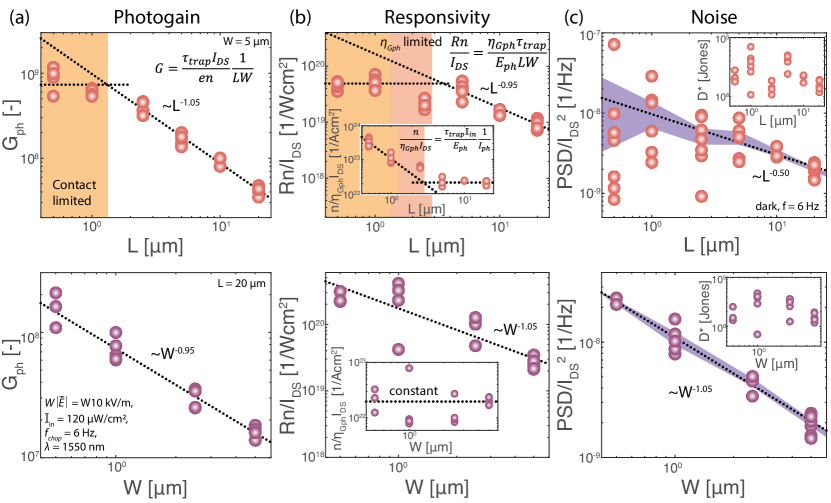
Next, the scaling of the photorespons by and was investigated as seen in Figure 4. For that devices with (number of devices) of 0.5 (5), 1 (6), 2.5 (4), 5 (5), 10 (3), and \qty20 (7) with a width of \qty5 were measured for the -scaling. For -scaling (number of devices) of 0.5 (3), 1 (5), 2.5 (4) and \qty5 (7) with a \qty20 were characterized. All the devices were on the same chip and had identical cQD film properties, allowing for a cross-comparison. The quantities , , where extracted from gate sweeps as described in Figure 2 (a). The values were taken at respective maximum photocurrent points in the p-doped region of graphene. As the photoresponse is proportional to , was scaled for a comparable current condition according to .
In Figure 4 (a), scaling by (top) and (bottom) is presented. A fit to the data (black dotted line) shows the trend and agrees with the prediction from equation (5). The horizontal dotted line indicates the mean value in that range. The scaling law breaks down around \qty1.5 (orange shaded region), where the total graphene FET resistance is about \qty2kΩ. This is comparable to the contact resistance of \qty1.2kΩ (\qty600Ω per contact) and thus points to a current injection limitation at the specified biasing condition. The -scaling follows a predicted trend over the evaluated region. As the -scaling devices have a \qty20, the smallest resistance for the \unit is about \qty8kΩ such that no current injection limitation is observed.
Figure 4 (b) depicts the scaling of photoresponsivity . The responsivity was normalized by to account for device-to-device variations (different residual doping levels) and contact resistance. follows also a -scaling law. Although is independent on geometry for constant , and thus
| (10) |
The breakdown of the scaling law, however, exceeds the current injection limited region caused by contacts (yellow shaded) and extends up to \qty3. The inset shows the normalization factor additionally accounting for . As is introduced, the red shaded area appears, thus being responsible for an additional length limitation to the scaling. The bottom panel shows the same normalized for the -scaling. In fact, as for the gain, there is a good agreement for the scaling observed over the investigated width scale. Moreover, the normalization factor, including , shows a constant trend. This highlights that might be similarly affected by reduced gatable channel lengths due to metal doping, as mentioned for above.
Finally, the influence of scaling on the noise and specific detectivity was investigated in Figure 4 (c). From normalized PSD spectra as shown in Figure 3 (d), the values at \qty6Hz were extracted for every device. The measurements were performed in dark and at the same gate voltage where the maximum photocurrent was extracted previously. The dotted lines show fits through the mean values of each length or width, whereas the purple shading indicates the standard deviation. The fits suggest a and dependence for the characterized devices. For the -scaling, the distribution of points increases as gets smaller, whereas the -scaling has an overall smaller spread of the data. The inset shows derived about \qty3e8Jones, using the photoresponse shown in (b).
Low frequency noise in GFETs is primarily attributed to electrostatic fluctuations arising from trap states at the oxide interface and leads to conductivity fluctuations in the channel.47, 51 Conductivity is related to the product of . Hence, the two main models that describe noise are based on (McWorther’s model) or (Hooge’s law) fluctuations.52, 47 Both models predict a dependence of noise in the FET channels.52 Accordingly, a volume scaling was experimentally verified for metallic break junctions to hold in the diffusive transport regime.53 For graphene FETs, however, the scaling has been found to experimentally not describe the data in full detail.54 Being restricted to a surface only, graphene is very sensitive to its environment. Thus, perturbations to the channel such as bilayers55, contacts56, 54, and environmental exposure54 are altering the electrostatic screening potential of the channel and influence the low-frequency noise. Like the photoresponse, though, reducing is pronouncing the contact effects. Hence, an increasing spread for smaller channels is observed. In addition, possible regions of double layers due to non-ideal CVD graphene growth and the additional current path through the cQD can thus be the reason for a deviation from an overall trend observed in the PSDs.
Expanding the demonstrated photocurrent characteristics of equation (6) into the detectivity yields
| (11) |
If now , there is no geometrical dependence expected in , which is consistent with the performed measurements. It is important to mention that the experimentally determined values between to \unitJones are around four orders of magnitude lower than the highest values found in the literature16 of \unitJones. The difference can be explained mainly by two factors from equation (11). First, the difference is in the found range. As does not differ much for devices with EHD printed (single step ligand exchange) and a LbL spin coated cQD films, the interface between graphene and cQD film limits most likely the charge transfer. CVD graphene processing is prone to defects and residuals from the growth and device fabrication. On the contrary, the highest values were reached with exfoliated single-crystal graphene. Second, defines the maximum reachable gain and is related to the photocurrent dynamics ( to relation). Preserving the magnitude for increasing leads to increasing due to lower noise in the channel as demonstrated in Figure 3 (c) and (d).
Conclusion
Here, the scaling of hybrid graphene-PbS cQD phototransistors with channel length , width , and cQD film thickness was experimentally demonstrated. The photocurrent was found to be independent of and but increased with . Instead, the photogain and responsivity scaled with . Although a dependence can be derived for , this neglects increasing channel currents with . Relating to leads to the relation. For , on the contrary, the geometrical dependence is evolving from a constant irradiance , rather than a constant light power seen by the detector. The scaling broke down for \unit due to contact metal contributions (contact resistance and channel doping). Although specific detectivity is , the found values in the range between to \unitJones ( \unitnm, \unitHz, room temperature) were independent on geometry. This is due to increasing noise currents for smaller dimensions. The photoresponse dependency on back gate voltage , bias , irradiance , and light chopping frequency were analyzed. A derived photogating efficiency of from those measurements pointed to a cQD-graphene interface limited charge transfer as a source for further photoresponse improvement.
Methods
Graphene Growth
CVD graphene was grown on commercial copper foil (Foil 2017, No. 46365, Alfa Aesar). The Cu-foil was first sonicated in acetone (\qty15min) and rinsed with deionized (DI) water. The foil was then immersed in nitric acid HNO3 (\qty30min), twice sonicated in DI-water (\qty1min), immersed in ethanol (\qty1min), and blow-dried with N2. The Cu-foil was annealed in H2 (\qty20sccm H2 and \qty200sccm Ar mixture) at \qty1000 and a pres-sure of \qty1mbar for \qty70min in a furnace. The graphene was grown from \qty0.04sccm methane CH4 for \qty21min at \qty1000 and a pressure of \qty110mbar, subsequentyl cooled down by opening the temperature shielding.
\AclGFET Fabrication
A p-Si substrate with \qty285nm chlorinated dry thermal SiO2 was prepatterned with contacts. The contacts were fabricated by e-beam-assisted thermal evaporation of Ti/Au (5/40 \unitnm) on a photolithographically defined resist (AZ5214E). PMMA 50K-protected graphene was prepared for wet transfer by Cu-etching in commercial Transene etchant (1 h), rinsed with DI water, left floating on hydrochloric acid (5 min), and re-rinsed with DI water. Graphene was transferred on the pre-patterned p-Si substrate from DI water, dried on a hotplate, and put into a vacuum (\qty60h). Graphene channels were O2-plasma etched using a Cu-mask, followed by Cr/Au top-contacts (2/40 \unitnm), both defined by e-beam lithography (PMMA 50K/PMMA 950K).
PbS cQD Film Fabrication
PbS QDs were synthesized following Hines et al. 57 with slight adaptations as described in detail previously29. For electrohydrodynamic nanoprinting (EHD), the PbS cQD were redispersed in n-tetradecane with a concentration of \qty40mg \perml and filtered with \qty0.1 PTFE syringe filter. Printing nozzles with openings between 2 to 3 \unitum were fabricated by pulling glass capillaries (World Precision Instruments TW100-4) and subsequent coating Ti/Au (5/\qty50nm). For the printing, the nozzle was brought in \unit proximity to the sample and an AC voltage of \qty280V (\qty250Hz) was applied between sample and nozzle. The structures were printed with a stage speed of \qty6\pers, line-spacing about \qty500nm, and subsequent overprinting was oriented in a staggered fashion. The EHD printing system used here was previously described in more detail.58 A single-step ligand exchange was performed by overnight soaking the cQD films in 2 vol% ethane-1,2-dithiol (EDT) in acetonitrile. Subsequently, the samples were rinsed in acetonitrile and dried with N2.
For the layer-by-layer (LbL) prepared film, the PbS cQDs were redispersed in octane with a concentration of \qty20mg \perml. A layer of PbS cQDs was spin-coated (\qty2500rpm, \qty45s), subsequently a drop of 2 vol% ethane-1,2-dithiol (EDT) in acetonitrile was placed for \qty30s before spinning the sample dry, and followed by one drop of acetonitrile and one drop of octane while sample was spinning (\qty2500rpm, \qty45s). The steps were repeated six times for a \unitnm film thickness.
Device Characterization
The GFET were electrical characterization before PbS cQD film deposition in a two-probe configuration (Keithley 4200-SCS semiconductor characterization system). The field-effect mobility was estimated by linear least squares fit (LSQ) to transfer curves ( vs. ). The contact resistance was estimated by the transfer length method (TLM).
To characterize the photoresponse, a broadband light source (Thorlabs, SLS201) was modulated with a chopper (Thorlabs, MC2000B-EC) and focused onto a monochromator (Princeton Instruments, SpectraPro HRS-300 spectrometer with grating 150 G/mm, blaze 0.8 \unit). Subsequent long-pass filters attenuated the higher spectral orders (400, 600, 800, 1200, 1900 nm) at the monochromator exit. The light was collimated with a lens and split with a 50/50 Polkadot beamsplitter. Onto one end, a reference detector (Gentec, UM-9B-L) was placed, and the light irradiance was determined by a lock-in amplifier (Stanford Research System, SR865A). Onto the other light path end, the samples were placed into an optically accessible cryostat (JANIS ST-100) with a quartz glass window. Gate voltage and source-drain bias were applied with SMUs (Keithley, 2614B and 2450). The photovoltage was measured over a shunt resistance of \qty1kΩ with lock-in amplifiers (Stanford Research System, SR860).
Noise currents were measured in the dark with a battery-powered trans-impedance amplifier (Stanford Research Systems, SR570). The signal was low pass filtered (10 kHz) and subsequently acquired with a data acquisition board (National Instruments, USB6341) at a sampling rate of 500 kHz. The DC offset was removed for the power spectral densities estimates, and one-second-long time traces were averaged.
All measurements were performed at room temperature and vacuum (4 mbar). The line frequency of \qty50Hz and its harmonic \qty150Hz were removed from all the frequency-dependent measurements. The measurements were repeated throughout the study duration for a selected set of devices ( \unitdays). In between the measurements, the samples were taken out of the measurement setup, rebonded in atmosphere, and placed back in the measurement setup. The measurements were reproducible with a maximal deviation of 30%. A device of each dimension was measured before the next one with the same dimension was investigated to reduce the influence of possible variation from sample alignment or degradation on the study outcome.
Acknowledgements
The authors thank FIRST-Lab (Center for Micro- and Nanoscience) at ETH Zurich for access to the clean-room and the Swiss National Science Foundation (SNSF, project no. 200021 182790) for financial support.
Author Contribution
G.K. and I.S. conceived the study and planned the experiments. G.K. fabricated the samples, performed the measurements and analyzed the data. P.R. performed the EHD printing with supervision by D.P. E.W. performed the FIB-SEM images. D.D. synthesized PbS colloidal QDs. R.F. grew graphene. G.K., I.S. and M.C. discussed the data. I.S., M.C., M.K, D.P. initated and supervised the project. G.K. wrote the manuscript with inputs and discussions from all authors.
References
- 1 M. V. Kovalenko, L. Manna, A. Cabot, Z. Hens, D. V. Talapin, C. R. Kagan, V. I. Klimov, A. L. Rogach, P. Reiss, D. J. Milliron, P. Guyot-Sionnnest, G. Konstantatos, W. J. Parak, T. Hyeon, B. A. Korgel, C. B. Murray, and W. Heiss, “Prospects of nanoscience with nanocrystals,” ACS Nano, vol. 9, no. 2, pp. 1012–1057, 2015.
- 2 H. Lu, G. M. Carroll, N. R. Neale, and M. C. Beard, “Infrared Quantum Dots: Progress, Challenges, and Opportunities,” ACS Nano, vol. 13, no. 2, pp. 939–953, 2019.
- 3 X. Tang, M. M. Ackerman, and P. Guyot-Sionnest, “Acquisition of Hyperspectral Data with Colloidal Quantum Dots,” Laser and Photonics Reviews, vol. 13, no. 11, 2019.
- 4 X. Tang, M. M. Ackerman, M. Chen, and P. Guyot-Sionnest, “Dual-band infrared imaging using stacked colloidal quantum dot photodiodes,” Nature Photonics, vol. 13, no. 4, pp. 277–282, 2019.
- 5 X. Tang, M. Chen, A. Kamath, M. M. Ackerman, and P. Guyot-Sionnest, “Colloidal Quantum-Dots/Graphene/Silicon Dual-Channel Detection of Visible Light and Short-Wave Infrared,” ACS Photonics, vol. 7, no. 5, pp. 1117–1121, 2020.
- 6 J. Gao, S. C. Nguyen, N. D. Bronstein, and A. P. Alivisatos, “Solution-Processed, High-Speed, and High-Quantum-Efficiency Quantum Dot Infrared Photodetectors,” ACS Photonics, vol. 3, no. 7, pp. 1217–1222, 2016.
- 7 M. Biondi, M. J. Choi, Z. Wang, M. Wei, S. Lee, H. Choubisa, L. K. Sagar, B. Sun, S. W. Baek, B. Chen, P. Todorović, A. M. Najarian, A. Sedighian Rasouli, D. H. Nam, M. Vafaie, Y. C. Li, K. Bertens, S. Hoogland, O. Voznyy, F. P. García de Arquer, and E. H. Sargent, “Facet-Oriented Coupling Enables Fast and Sensitive Colloidal Quantum Dot Photodetectors,” Advanced Materials, vol. 33, no. 33, 2021.
- 8 M. Vafaie, J. Z. Fan, A. Morteza Najarian, O. Ouellette, L. K. Sagar, K. Bertens, B. Sun, F. P. García de Arquer, and E. H. Sargent, “Colloidal quantum dot photodetectors with 10-ns response time and 80% quantum efficiency at 1,550 nm,” Matter, vol. 4, no. 3, pp. 1042–1053, 2021.
- 9 A. A. Bessonov, M. Allen, Y. Liu, S. Malik, J. Bottomley, A. Rushton, I. Medina-Salazar, M. Voutilainen, S. Kallioinen, A. Colli, C. Bower, P. Andrew, and T. Ryhänen, “Compound Quantum Dot-Perovskite Optical Absorbers on Graphene Enhancing Short-Wave Infrared Photodetection,” ACS Nano, vol. 11, no. 6, pp. 5547–5557, 2017.
- 10 X. Tang, M. M. Ackerman, G. Shen, and P. Guyot-Sionnest, “Towards Infrared Electronic Eyes: Flexible Colloidal Quantum Dot Photovoltaic Detectors Enhanced by Resonant Cavity,” Small, vol. 15, no. 12, 2019.
- 11 E. O. Polat, G. Mercier, I. Nikitskiy, E. Puma, T. Galan, S. Gupta, M. Montagut, J. J. Piqueras, M. Bouwens, T. Durduran, G. Konstantatos, S. Goossens, and F. Koppens, “Flexible graphene photodetectors for wearable fitness monitoring,” Science Advances, vol. 5, no. 9, 2019.
- 12 J. Kim, S.-M. Kwon, Y. K. Kang, Y.-H. Kim, M.-J. Lee, K. Han, A. Facchetti, M.-G. Kim, and S. K. Park, “A skin-like two-dimensionally pixelized full-color quantum dot photodetector,” Science Advances, vol. 5, p. eaax8801, aug 2023.
- 13 J. S. Steckel, E. Josse, A. G. Pattantyus-Abraham, M. Bidaud, B. Mortini, H. Bilgen, O. Arnaud, S. Allegret-Maret, F. Saguin, L. Mazet, S. Lhostis, T. Berger, K. Haxaire, L. L. Chapelon, L. Parmigiani, P. Gouraud, M. Brihoum, P. Bar, M. Guillermet, S. Favreau, R. Duru, J. Fantuz, S. Ricq, D. Ney, I. Hammad, D. Roy, A. Arnaud, B. Vianne, G. Nayak, N. Virollet, V. Farys, P. Malinge, A. Tournier, F. Lalanne, A. Crocherie, J. Galvier, S. Rabary, O. Noblanc, H. Wehbe-Alause, S. Acharya, A. Singh, J. Meitzner, D. Aher, H. Yang, J. Romero, B. Chen, C. Hsu, K. C. Cheng, Y. Chang, M. Sarmiento, C. Grange, E. Mazaleyrat, K. Rochereau, Jonathan Steckel, E. Josse, A. G. Pattantyus-Abraham, M. Bidaud, B. Mortini, H. Bilgen, O.Arnaud, J. S. Steckel, E. Josse, A. G. Pattantyus-Abraham, M. Bidaud, B. Mortini, H. Bilgen, O. Arnaud, S. Allegret-Maret, F. Saguin, L. Mazet, S. Lhostis, T. Berger, K. Haxaire, L. L. Chapelon, L. Parmigiani, P. Gouraud, M. Brihoum, P. Bar, M. Guillermet, S. Favreau, R. Duru, J. Fantuz, S. Ricq, D. Ney, I. Hammad, D. Roy, A. Arnaud, B. Vianne, G. Nayak, N. Virollet, V. Farys, P. Malinge, A. Tournier, F. Lalanne, A. Crocherie, J. Galvier, S. Rabary, O. Noblanc, H. Wehbe-Alause, S. Acharya, A. Singh, J. Meitzner, D. Aher, H. Yang, J. Romero, B. Chen, C. Hsu, K. C. Cheng, Y. Chang, M. Sarmiento, C. Grange, E. Mazaleyrat, and K. Rochereau, “1.62µm Global Shutter Quantum Dot Image Sensor Optimized for Near and Shortwave Infrared,” Technical Digest - International Electron Devices Meeting, IEDM, pp. 518–521, 2021.
- 14 C. Gréboval, A. Chu, D. V. Magalhaes, J. Ramade, J. Qu, P. Rastogi, A. Khalili, S. S. Chee, H. Aubin, G. Vincent, S. Bals, C. Delerue, and E. Lhuillier, “Ferroelectric Gating of Narrow Band-Gap Nanocrystal Arrays with Enhanced Light-Matter Coupling,” ACS Photonics, vol. 8, no. 1, pp. 259–268, 2021.
- 15 T. H. Dang, C. Abadie, A. Khalili, C. Gréboval, H. Zhang, Y. Prado, X. Z. Xu, D. Gacemi, A. Descamps-Mandine, S. Ithurria, Y. Todorov, C. Sirtori, A. Vasanelli, and E. Lhuillier, “Broadband Enhancement of Mid-Wave Infrared Absorption in a Multi-Resonant Nanocrystal-Based Device,” Advanced Optical Materials, vol. 10, no. 9, 2022.
- 16 G. Konstantatos, M. Badioli, L. Gaudreau, J. Osmond, M. Bernechea, F. P. G. De Arquer, F. Gatti, and F. H. Koppens, “Hybrid graphene–quantum dot phototransistors with ultrahigh gain,” Nature Nanotechnology, vol. 7, no. 6, pp. 363–368, 2012.
- 17 Z. Sun, Z. Liu, J. Li, G. A. Tai, S. P. Lau, and F. Yan, “Infrared photodetectors based on CVD-grown graphene and PbS quantum dots with ultrahigh responsivity,” Advanced Materials, vol. 24, no. 43, pp. 5878–5883, 2012.
- 18 D. Kufer, I. Nikitskiy, T. Lasanta, G. Navickaite, F. H. Koppens, and G. Konstantatos, “Hybrid 2D-0D MoS2-PbS quantum dot photodetectors,” Advanced Materials, vol. 27, no. 1, pp. 176–180, 2015.
- 19 D. Kufer, T. Lasanta, M. Bernechea, F. H. Koppens, and G. Konstantatos, “Interface Engineering in Hybrid Quantum Dot-2D Phototransistors,” ACS Photonics, vol. 3, no. 7, pp. 1324–1330, 2016.
- 20 O. Özdemir, I. Ramiro, S. Gupta, and G. Konstantatos, “High Sensitivity Hybrid PbS CQD-TMDC Photodetectors up to 2 m,” ACS Photonics, vol. 6, no. 10, pp. 2381–2386, 2019.
- 21 B. Kundu, O. Özdemir, M. Dalmases, G. Kumar, and G. Konstantatos, “Hybrid 2D-QD MoS2–PbSe Quantum Dot Broadband Photodetectors with High-Sensitivity and Room-Temperature Operation at 2.5 µm,” Advanced Optical Materials, vol. 9, no. 22, 2021.
- 22 H. T. Choi, J. H. Kang, J. Ahn, J. Jin, J. Kim, S. Park, Y. H. Kim, H. Kim, J. D. Song, G. W. Hwang, S. Im, W. Shim, Y. T. Lee, M. C. Park, and D. K. Hwang, “Zero-Dimensional PbS Quantum Dot-InGaZnO Film Heterostructure for Short-Wave Infrared Flat-Panel Imager,” ACS Photonics, vol. 7, no. 8, pp. 1932–1941, 2020.
- 23 S. Ahn, W. Chen, M. A. Moreno-Gonzalez, M. Lockett, J. Wang, and O. Vazquez-Mena, “Enhanced Charge Transfer and Responsivity in Hybrid Quantum Dot/Graphene Photodetectors Using ZnO as Intermediate Electron-Collecting Layer,” Advanced Electronic Materials, vol. 6, no. 6, 2020.
- 24 S. Ahn and O. Vazquez-Mena, “Measuring the carrier diffusion length in quantum dot films using graphene as photocarrier density probe,” Journal of Chemical Physics, vol. 156, no. 2, 2022.
- 25 I. Nikitskiy, S. Goossens, D. Kufer, T. Lasanta, G. Navickaite, F. H. Koppens, and G. Konstantatos, “Integrating an electrically active colloidal quantum dot photodiode with a graphene phototransistor,” Nature Communications, vol. 7, no. 1, 2016.
- 26 M. J. Grotevent, C. U. Hail, S. Yakunin, D. Bachmann, M. Calame, D. Poulikakos, M. V. Kovalenko, and I. Shorubalko, “Colloidal HgTe Quantum Dot/Graphene Phototransistor with a Spectral Sensitivity Beyond 3 µm,” Advanced Science, vol. 8, no. 6, 2021.
- 27 Z. Ni, L. Ma, S. Du, Y. Xu, M. Yuan, H. Fang, Z. Wang, M. Xu, D. Li, J. Yang, W. Hu, X. Pi, and D. Yang, “Plasmonic Silicon Quantum Dots Enabled High-Sensitivity Ultrabroadband Photodetection of Graphene-Based Hybrid Phototransistors,” ACS Nano, vol. 11, no. 10, pp. 9854–9862, 2017.
- 28 M. J. Grotevent, C. U. Hail, S. Yakunin, D. N. Dirin, K. Thodkar, G. Borin Barin, P. Guyot-Sionnest, M. Calame, D. Poulikakos, M. V. Kovalenko, and I. Shorubalko, “Nanoprinted Quantum Dot–Graphene Photodetectors,” Advanced Optical Materials, vol. 7, no. 11, 2019.
- 29 G. Kara, S. Bolat, K. Sharma, M. J. Grotevent, D. N. Dirin, D. Bachmann, R. Furrer, L. F. Boesel, Y. E. Romanyuk, R. M. Rossi, M. V. Kovalenko, M. Calame, and I. Shorubalko, “Conformal Integration of an Inkjet-Printed PbS QDs-Graphene IR Photodetector on a Polymer Optical Fiber,” Advanced Materials Technologies, vol. 2201922, 2023.
- 30 F. H. Koppens, T. Mueller, P. Avouris, A. C. Ferrari, M. S. Vitiello, and M. Polini, “Photodetectors based on graphene, other two-dimensional materials and hybrid systems,” Nature Nanotechnology, vol. 9, no. 10, pp. 780–793, 2014.
- 31 R. Saran and R. J. Curry, “Lead sulphide nanocrystal photodetector technologies,” Nature Photonics, vol. 10, no. 2, pp. 81–92, 2016.
- 32 N. Huo and G. Konstantatos, “Recent progress and future prospects of 2D-based photodetectors,” Advanced Materials, vol. 30, no. 51, 2018.
- 33 H. Fang and W. Hu, “Photogating in Low Dimensional Photodetectors,” Advanced Science, vol. 4, no. 12, 2017.
- 34 B. E. A. Saleh and M. C. Teich, Fundamentals of photonics. Wiley series in pure and applied optics, Hoboken, New Jersey: Wiley, 2nd ed., 2007.
- 35 I. Moreels, K. Lambert, D. Smeets, D. De Muynck, T. Nollet, J. C. Martins, F. Vanhaecke, A. Vantomme, C. Delerue, G. Allan, and Z. Hens, “Size-dependent optical properties of colloidal PbS quantum dots,” ACS Nano, vol. 3, no. 10, pp. 3023–3030, 2009.
- 36 P. Galliker, J. Schneider, H. Eghlidi, S. Kress, V. Sandoghdar, and D. Poulikakos, “Direct printing of nanostructures by electrostatic autofocussing of ink nanodroplets,” Nature Communications, vol. 3, no. 1, 2012.
- 37 M. S. Onses, E. Sutanto, P. M. Ferreira, A. G. Alleyne, and J. A. Rogers, “Mechanisms, Capabilities, and Applications of High-Resolution Electrohydrodynamic Jet Printing,” Small, vol. 11, no. 34, pp. 4237–4266, 2015.
- 38 J. M. Luther, M. Law, Q. Song, C. L. Perkins, M. C. Beard, and A. J. Nozik, “Structural, Optical, and Electrical Properties of Self-Assembled Films of PbSe Nanocrystals Treated with 1,2-Ethanedithiol,” ACS Nano, vol. 2, pp. 271–280, feb 2008.
- 39 C. H. M. Chuang, P. R. Brown, V. Bulović, and M. G. Bawendi, “Improved performance and stability in quantum dot solar cells through band alignment engineering,” Nature Materials, vol. 13, no. 8, pp. 796–801, 2014.
- 40 M. Albaladejo-Siguan, E. C. Baird, D. Becker-Koch, Y. Li, A. L. Rogach, and Y. Vaynzof, “Stability of Quantum Dot Solar Cells: A Matter of (Life)Time,” Advanced Energy Materials, vol. 11, no. 12, 2021.
- 41 Z. Wu, Y. Ou, M. Cai, Y. Wang, R. Tang, and Y. Xia, “Short-Wave Infrared Photodetectors and Imaging Sensors Based on Lead Chalcogenide Colloidal Quantum Dots,” Advanced Optical Materials, vol. 11, no. 1, 2023.
- 42 Y. Q. Huang, R. J. Zhu, N. Kang, J. Du, and H. Q. Xu, “Photoelectrical response of hybrid graphene-PbS quantum dot devices,” Applied Physics Letters, vol. 103, no. 14, 2013.
- 43 X. Du, I. Skachko, A. Barker, and E. Y. Andrei, “Approaching ballistic transport in suspended graphene,” Nature Nanotechnology, vol. 3, no. 8, pp. 491–495, 2008.
- 44 A. Dorodnyy, Y. Salamin, P. Ma, J. Vukajlovic Plestina, N. Lassaline, D. Mikulik, P. Romero-Gomez, A. Fontcuberta i Morral, and J. Leuthold, “Plasmonic Photodetectors,” IEEE Journal of Selected Topics in Quantum Electronics, vol. 24, no. 6, 2018.
- 45 M. J. Grotevent, C. U. Hail, S. Yakunin, D. Bachmann, G. Kara, D. N. Dirin, M. Calame, D. Poulikakos, M. V. Kovalenko, and I. Shorubalko, “Temperature-Dependent Charge Carrier Transfer in Colloidal Quantum Dot/Graphene Infrared Photodetectors,” ACS Applied Materials & Interfaces, vol. 13, pp. 848–856, jan 2021.
- 46 R. Wang, Y. T. Zhang, H. Y. Wang, X. X. Song, L. F. Jin, and J. Q. Yao, “Wide spectral response field-effect phototransistor based on graphene-quantum dot hybrid,” IEEE Photonics Journal, vol. 7, no. 2, 2015.
- 47 A. A. Balandin, “Low-frequency 1/f noise in graphene devices,” Nature Nanotechnology, vol. 8, no. 8, pp. 549–555, 2013.
- 48 R. H. Bube, Photoconductivity of solids. New York: Wiley, 2nd ed., 1967.
- 49 G. Konstantatos and E. H. Sargent, “PbS colloidal quantum dot photoconductive photodetectors: Transport, traps, and gain,” Applied Physics Letters, vol. 91, no. 17, p. 173505, 2007.
- 50 F. Xia, T. Mueller, R. Golizadeh-Mojarad, M. Freitage, Y. M. Lin, J. Tsang, V. Perebeinos, and P. Avouris, “Photocurrent imaging and efficient photon detection in a graphene transistor,” Nano Letters, vol. 9, no. 3, pp. 1039–1044, 2009.
- 51 P. Karnatak, T. Paul, S. Islam, and A. Ghosh, “1/f noise in van der Waals materials and hybrids,” Advances in Physics: X, vol. 2, no. 2, pp. 428–449, 2017.
- 52 E. Simoen and C. Claeys, “On the flicker noise in submicron silicon MOSFETs,” Solid-State Electronics, vol. 43, no. 5, pp. 865–882, 1999.
- 53 Z. Wu, S. Wu, S. Oberholzer, M. Steinacher, M. Calame, and C. Schönenberger, “Scaling of 1/f noise in tunable break junctions,” Physical Review B, vol. 78, no. 23, 2008.
- 54 S. Rumyantsev, G. Liu, W. Stillman, M. Shur, and A. A. Balandin, “Electrical and noise characteristics of graphene field-effect transistors: Ambient effects, noise sources and physical mechanisms,” Journal of Physics Condensed Matter, vol. 22, no. 39, 2010.
- 55 I. Heller, S. Chatoor, J. Männik, M. A. Zevenbergen, J. B. Oostinga, A. F. Morpurgo, C. Dekker, and S. G. Lemay, “Charge noise in graphene transistors,” Nano Letters, vol. 10, no. 5, pp. 1563–1567, 2010.
- 56 P. Karnatak, T. P. Sai, S. Goswami, S. Ghatak, S. Kaushal, and A. Ghosh, “Current crowding mediated large contact noise in graphene field-effect transistors,” Nature Communications, vol. 7, no. 1, 2016.
- 57 M. A. Hines and G. D. Scholes, “Colloidal PbS Nanocrystals with Size-Tunable Near-Infrared Emission: Observation of Post-Synthesis Self-Narrowing of the Particle Size Distribution,” Advanced Materials, vol. 15, no. 21, pp. 1844–1849, 2003.
- 58 F. V. Antolinez, J. M. Winkler, P. Rohner, S. J. P. Kress, R. C. Keitel, D. K. Kim, P. Marqués-Gallego, J. Cui, F. T. Rabouw, D. Poulikakos, and D. J. Norris, “Defect-Tolerant Plasmonic Elliptical Resonators for Long-Range Energy Transfer,” ACS Nano, vol. 13, pp. 9048–9056, aug 2019.