Comparative study of quantum emitter fabrication in wide bandgap materials using localized electron irradiation
Abstract
Quantum light sources are crucial foundational components for various quantum technology applications. With the rapid development of quantum technology, there has been a growing demand for materials that are capable of hosting quantum emitters. One such material platforms are fluorescent defects in hexagonal boron nitride (hBN) inducing deep sub-levels within the band gap. The question arises if other layered wide bandgap (2D) materials offer similar single photon emitting defects. Here, we investigate and compare the fabrication of quantum emitters in exfoliated multi-layer mica flakes with hBN and other wide bandgap 3D crystals (silicon carbide and gallium nitride) which are known to host quantum emitters. We use our primary fabrication technique of localized electron irradiation using a standard scanning electron microscope. To complement our experimental work, we employ density functional theory simulations to study the atomic structures of intrinsic defects and their photophysical properties. While our fabrication technique can create hBN quantum emitters with a high yield and high single photon purity, it is unable to fabricate emitters in the other solid-state crystals under investigation. This allows us to draw conclusions on the emitter fabrication mechanism, which could be relying on the activation of already present defects by charge state manipulation. We therefore provide an important step toward the identification of hBN emitters and their formation process.
I Introduction
Quantum emitters in solid-state crystals have garnered considerable attention, driven by the rapid advancement of quantum technology applications such as quantum computing, quantum communication, and quantum sensing [1, 2, 3, 4, 5]. The discovery of quantum emitters based on defects in wide bandgap materials has significantly advanced this field [6, 7, 8, 9, 10, 11]. Quantum emitters have been used in a wide variety of applications, most prominently in magnetometry and imaging [12, 13], but also in quantum key distribution [4, 5], fundamental quantum physics tests [14], thermometry [15], pressure sensing [16], quantum computing [17], quantum memories [18, 19, 20], and as nodes in a quantum network [21].
Probably the most-well studied solid-state quantum emitter is the nitrogen vacancy center in diamond [22] and related defects, such as the group-IV color centers [23]. Quantum emitters in two-dimensional materials such as semiconducting transition metal dichalcogenides (TMDs) [24, 25] and insulating hexagonal boron nitride (hBN) [6, 7] offer the advantage of intrinsically high photon out-coupling, as a defect in an atomically thin material is not surrounded by any high refractive index and therefore not limited by any total internal or Fresnel reflection [26]. In addition, 2D materials can be easily attached to photonic components through van der Waals forces, making them outstanding candidates for integrated photonics and waveguides platforms [27].
The quantum emitters can be fabricated using various methods such as strain activation using nanostructure [24], mechanical damage using the tip of an atomic force microscope (AFM) [28], thermal activation of naturally occurring defects [7], plasma [29] and chemical etching [30], as well as energetic irradiation [25, 31, 32, 33, 34]. Of particular interest is the formation of emitters at pre-defined locations, while minimizing the impact of the crystal environment, for which localized irradiation has shown to be useful. The response of materials to the irradiation by energetic particles such as electrons and ions has been studied intensively [35]. Irradiation can create new defects in solids by knocking out atoms or implanting impurities, but also modify or activate existing defects by breaking and re-organizing bonds or changing the charge state. This can ultimately result in the modification of their physical and chemical properties. Recent works have shown the high yield of quantum emitters in TMDs and hBN by modifying the surface properties or doping [33, 32, 25, 34] and arrays of photophysically identical emitters with correlated dipoles [36], all using electron irradiation of hBN or a focused helium beam in case of MoS2.
The emitter formation process using electron irradiation in hBN is not well understood. Not only differ the emitters in terms of formation depth [26] compared to other fabrication methods, but also the emitter properties differ when comparing the photophysical properties of electron beam irradiated hBN emitters in different works: some have basically random-oriented dipoles [37] while others have correlated dipole directions [36]; or some emit blue light [33, 32], and others have their optical transition in the yellow region [34, 36]. The question arises how unique the electron irradiation process is to hBN or if it can be applied to other wide bandgap materials as well.
In this work, we carry out a comprehensive study and compare our electron irradiation fabrication method on hBN [32, 33, 34] with other wide bandgap materials, including 2D mica muscovite with a bandgap around 5 eV [38, 39], as well as the 3D crystals silicon carbide and gallium nitride. Both the latter are well known to host optically active quantum emitters [9, 10, 40, 8, 11, 41], while in the case of mica, only fluorescent molecules adhering to the surface have been shown to support quantum emission [42]. By using different materials and crystals (of the same type) but from different vendors, we gain insight into the emitter formation process. We first fabricate an array of high quality quantum emitters in hBN and then replicate the same fabrication process on a large variety of samples. In addition, we also try high temperature annealing and check if any newly created defects require thermal activation. Our experiments and conclusions are supported using density functional theory (DFT) calculations, which reveal the electronic structure of potential defects in mica and allow us to infer if the defect should be optically active or not. Finally, we draw conclusions about the quantum emitter formation process in hBN.
II Experimental details
II.1 Sample preparation
To create hBN emitters, we first mechanically exfoliate from bulk crystal onto an organic polymer sheet made of PDMS (polydimethylsiloxane) using a scotch tape. Afterwards, a suitable thin flake is transfer onto a grid patterned standard silicon substrate with a 290 nm thermal oxide layer by dry stamping (see Methods). We have used bulk hBN from HQ Graphene (named hBN-1 in the following) and 2D Semiconductors (hBN-2), which produce their crystals using different processes, e.g., 2D Semiconductors utilize a high-pressure anvil cell growth method. It is therefore likely that the samples have a different intrinsic doping of impurities.
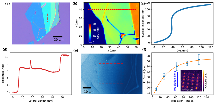
The mica muscovite flakes are exfoliated and transferred in the same fashion as mentioned above. Fig. 1(a) shows an optical image of a transferred mica flake. The thickness map is created using a phase-shift interferometer (PSI) that measures the optical path length (OPL) through the flake and is shown in Fig. 1(b). To convert the OPL measurements into physical thickness values, rigorous coupled-wave analysis (RCWA) simulations are used, similarly as it has been done before for TMDs [43] and hBN [29]. The RCWA model shown in Fig. 1(c) is calibrated using real thickness measurements obtained with an AFM (see Supplementary Section S1). Once the RCWA model is calibrated, using the PSI proves to be both accurate and faster than the commonly employed AFM thickness measurements [43, 29, 26]. It is important to note, however, that this technique can only yield accurate results for OPL thicknesses up to 30 nm (for mica on silicon substrate with a 290 nm thermal oxide layer), as the relation between physical and optical thickness follows an S-curve due to interference (see Fig. 1(c)). The physical flake thickness through the dashed line in the OPL map is shown in Fig. 1(d). The flake on which the subsequent electron irradiation is carried out has a thickness around 6 nm (blue area in the microscope image) and around 10 nm (teal area in the microscope image).
The 3D crystals, silicon carbide (4H) and gallium nitride (n-type doped on sapphire), were directly acquired from MSE Supplies and used as received.
II.2 Electron irradiation
We performed localized electron irradiation using a SEM to deliberately introduce defect-based quantum emitters into the materials. This method has demonstrated its effectiveness in creating quantum emitters within hBN, as substantiated by prior studies [32, 33, 34]. The high lateral resolution of SEM allow us to irradiate the exfoliated multi-layer mica flake at a chosen spot as shown in Figure 1(e). The irradiated spots are clearly visible in the resulting SEM image post irradiation process. Here each spot is irradiated using an accelerating voltage of 3 kV and electron current of 25 pA with a dwell time of 10 s (see Methods). This resulted an electron fluence of cm-2 at each irradiated spot. Note that we used low electron fluence (1013 cm-2) is used to record the image of the flake in order to avoid the creation of randomly located emitters in the flake, due to electron beam scanning during imaging process.
To control the electron dose precisely, we adjust the irradiation time during the irradiation process. Additionally, we performed the irradiation process with varying electron irradiation times on one of the flakes. The resulting PL map of the irradiated spot within the flake is displayed in the inset of Figure 1(f). To calculate the average PL intensity, we took the mean across the same number of pixels for each spot (see Supplementary Section S2). The observed behaviour is quite intriguing; the average PL intensity exhibits saturation tendencies with increasing irradiation time, as depicted in Figure 1(f). This behaviour suggests that the creation of defects in the mica flake is constrained by an upper limit, resembling the controlled creation of emitters in hBN through the irradiation process [44, 34]. These findings underscore the precision and controllability of defect engineering within the mica flakes, promising exciting prospects for applications in quantum emitters fabrication.
III Results and discussions
III.1 Optical characterization
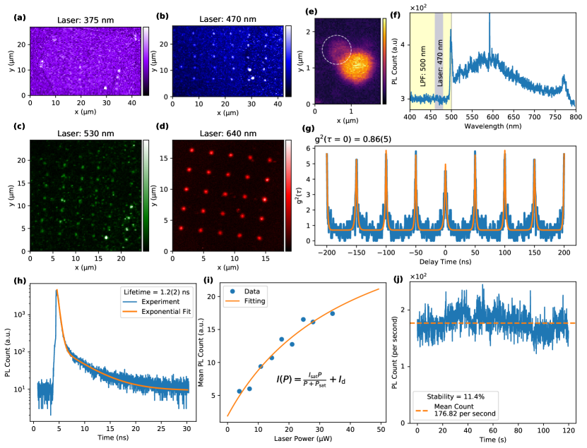
To investigate our fabrication methodology of quantum emitters, we optically characterized the samples using a commercial fluorescence lifetime imaging microscope (see Methods). We first investigated irradiated mica flakes. We performed all the measurements at room temperature using different pulsed excitation lasers with a repetition rate of 20 MHz. We always excite below bandgap to exclusively excite any states that were created during the irradiation process and at the same time to avoid the bandgap excitation of the free exciton. Figures 2(a)-(d) present the PL maps of the samples using 375 nm, 470 nm, 530 nm and 640 nm pulsed excitation lasers, respectively. Under 375 nm excitation laser, we observe weak emission from the irradiated spots indicating very inefficient excitation in the UV region. However, we notice bright emission from the irradiated spots under different excitation lasers as shown in Figure 2(b)-(d). Bright emission in the PL map corresponds to the irradiated spots as can be confirmed by SEM and PL images. We also did not observe any correlation in between bright emission from irradiated spots and the flake thickness.
Furthermore, we see diffraction-limited isolated spots in the close vicinity of the irradiated spots as shown in Figure 1(e), when a zoomed-in PL map is created using 470 nm pulsed excitation laser. This is similar to the previously studied hBN irradiation experiments, which were responsible for the generation of blue and yellow single photon emitters around the irradiated spots [32, 33, 34, 36]. However, we did not find any sharp spectral feature as recorded under 470 nm excitation laser in combination with a long pass filter with a cut-off wavelength at 500 nm to suppress the excitation laser. We rather observe a broad peak centered around 600 nm as shown in Figure 2(f). This emission behaviour resembles what we observed from the irradiated spots in hBN in our previous works [34, 36]. This could be an indication that our irradiation process may indeed lead to the formation of similar defect complexes in mica as well upon electron irradiation, potentially due to deposited carbon [34]. Note that due to the relatively weak PL emission, we extended the exposure time to acquire the spectrum effectively. As a result of this longer exposure time, we also captured certain experimental artefact peaks in our measurements. Notably, these artefact peaks were also present in our background spectrum measurements, which were taken at a location away from the irradiated spot and subjected to the same extended exposure time (see Supplementary Section S3).
In order to further investigate the quantum nature of emission, we measure the second-order correlation function (g(2)) from the various irradiated spots. In Figure 2(e), we present an experimentally measured g(2) curve, acquired using a 470 nm pulsed excitation laser with a repetition rate of 20 MHz. To analyze the data, we employed a model function to fit the g(2) curve and extracted a g around 0.86(5), which is larger than 0.5 (the generally accepted criterion for single photon emission due to a non-zero overlap with the single photon Fock state). Unlike a previous recent studies which introduced organic fluorescent molecules from solvents [42], we have not been able to create single emitters in mica using our electron irradiation process. We have also measured the excited state lifetime of the emitter to be around 1.2 ns. The lifetime decay curve is fitted using a bi-exponential function to extract the lifetime as shown in Figure 2(h). Note that the initial sharp peak is due to instrument response function and taken care of in our fitting routine. Additionally, We examined the intensity from the irradiated spot as a function of excitation laser power, revealing the typical saturation curve for two level system, as depicted in Figure 2(i). We fitted the experimental data using a model function revealing the average saturation power to be around 40.75 W and saturation intensity is 35.18 counts per second. Remarkably, our experimental observation did not reveal any photo-bleaching or blinking. effects under pulsed excitation. We measured the photon count rate over an extended time period as shown in Figure 2(j), and this revealed a stable emission with a stability of 11.4%.
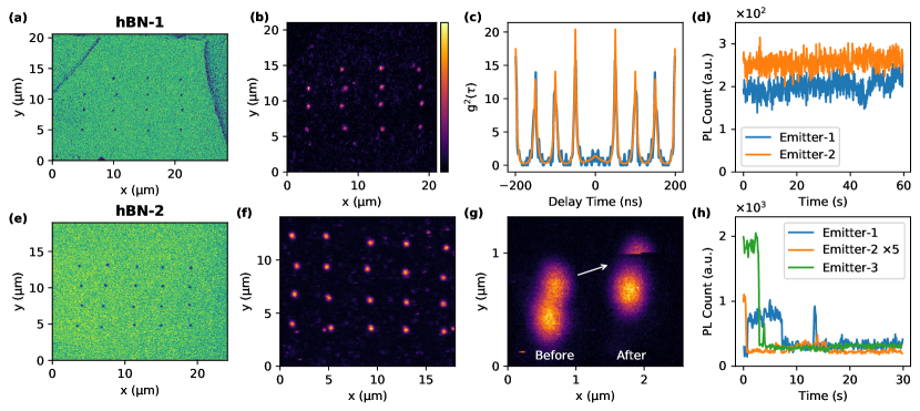
To gain deeper insights into the generality of our fabrication methodology in generating quantum emitters, we extended our irradiation experiment on various other insulating materials including two-dimensional hBN-1, hBN-2, silicon carbide (4H-SiC) and gallium nitride (GaN) crystals. For hBN-1, we initially exfoliated a multi-layer flake onto a standard Si/SiO2 substrate and conducted localized irradiation at a chosen spot within the flake, employing a dwell time of 10 seconds. This resulted in a similar electron fluence as in the case of mica irradiation. The resulting SEM of the flake is shown in Figure 3(a) (see Methods). Subsequently, we recorded the PL map of the irradiated flake using 530 nm pulsed excitation laser as shown in Figure 3(b). It is evident that the bright spot in the PL map corresponds to the irradiated spots in the SEM images. Our irradiation process effectively yielded emitters emitting at 575 nm [34].
To further understand the quantum nature of emission, we performed g(2) measurements using 530 nm pulsed excitation laser with a repetition rate of 20 MHz. The results, displayed in Figure 3(c), reveal a clear g(2) dip with a g(2)(0) value of 0.084(2), as extracted from the model fitting function. We also noticed a stable emission from the quantum emitters with no instances of blinking and photo-bleaching as observed in Figure 3(d). The further photo-physical properties of as fabricated emitters are also summarized in the our previous works [34, 36].
For hBN-2, we performed the localized irradiation with the same electron beam parameters using the same process on the same SEM. Figure 3(a) shows the SEM images of an irradiated sample. The irradiated spots are clearly visible as distinctive dots. The corresponding PL map, depicted in Figure 3(b), also reveals bright emissions emanating from the irradiated spots. The PL map is created using 530 nm pulsed excitation laser with the similar laser power. This indicates the generation of similar defect complex formation due to localized irradiation. The zoomed-in PL map around one of the irradiated spot also reveals the formation of isolated diffraction limited spot, indicating the formation of an isolated emitter as observe for hBN-1. However, in the consecutive PL map in Figure 3(c) shows that emitter bleached out eventually.
Furthermore, we investigated other emitters around the irradiated spots and recorded the PL count rate over time. and found that these emitters are not stable once excited. We observed the PL counts drop down to the noise level of the detector within the 10 s (see Supplementary Section S3). Such instability has not been observed for the emitters in hBN-1 under pulsed excitation even after prolonged exposure. Notably, we also observed no aging effect on the emitters in hBN-1. This instability observed in hBN-2 could be attributed to unstable charge carriers in the excited state potentially due to intrinsic doping of the material which depends on the growth conditions.
In addition to the hBN, our irradiation experiment of SiC (4H-semi insulating) and GaN do not activate any emitters or emitters ensembles as evident by PL map (see Supplementary Section S4). We found that this is independent of the electron beam dose and electron accelerating voltage. We can draw already two summarizing conclusions from our experiments: (i) the electron irradiation process works very well to generate single photon emitters in hBN but not in other wide bandgap materials. This indicates that, at least in this fabrication method, lattice defects and not deposited complexes on the surface. If the latter was the case, this should also work on other materials as a substrate. And (ii), while we could create single photon emitters in both hBN samples, there seems to be a different intrinsic defect density that instabilizes the defects in hBN-2.
III.2 Theoretical calculations
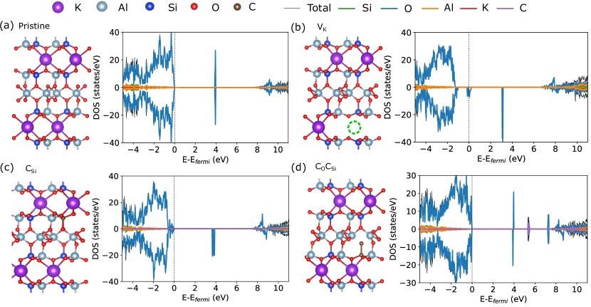
For hBN it is known to host a large variety of optically active emitters [45]. The question arises if this is true for mica as well. This would determine if our fabrication method simply does not work on mica or that there are generally not many optically active defects. To calculate the optical signatures, we employed density functional theory (DFT) calculations (See Methods for the computational details). Here, we take into account the spin polarization as, for the allowed optical transition, it should be preserved. Figure 4(a) depicts the electronic structure of the pristine mica with a bandgap of 7.91 eV. Due to this wide gap property, mica should in principle support defect levels similar to other wide bandgap materials just like hBN [45, 46, 47] and diamond [48, 49, 50]. In these materials, single photon emission originates from a transition between two-level states of occupied and unoccupied defect states, unlike TMDs that are some time from the transition between strained valence and conduction bands [51, 52]. As a consequence, we calculate 20 different types of point defects, mostly native and antisite defects but also carbon impurities, since a scanning electron microscope typically bonds carbon to the surface [34]. For this, we aimed to investigate the existence of two-level states localized far away from the valence and conduction bands greater than 1 eV, the so-called deep-lying defect states.
In Figure 4(b), the V defect introduces two-level states between occupied and unoccupied states contributed by oxygen atoms. However, these are shallow levels which have full occupation at room temperature. Considering a carbon dopant at different sites in Figures 4(c) and (d), both cases do not exhibit any two-level states. Although it likely has an unoccupied state at 5 eV, which can accept some excited electrons, this large transition energy is out of reach for our experiments. In addition, we expect that this system would have a low transition rate. Together with the absence of an occupied isolated defect state, both are unlikely to act as a single photon emitter. It is worth noting that all defects seem not to localize at both bottom-most and top-most states. This indicates that the defect in mica has little influence on deep-lying two-level states. All these behaviors have also been observed in the rest of the defects shown in Supplementary S6 except for Al, where its desired two-level states exist. Thus, this implies that mica hosts many optically inactive defects compared to hBN [45, 47]. As a result, it can be concluded that although mica offers a wide bandgap, which in principle can host many defects, electronic states of those doped defects do not appear in the bandgap region, but rather around the valence and conduction bands. In other words, mica is not a feasible material to support single photon emitters, at least not as suitable as hBN.
IV Conclusion
We extensively demonstrate the investigation of quantum emitters through a localized irradiation process and have provided a valuable insights into the effectiveness of this methodology across the various insulating materials. We ventured beyond mica and explored other insulating materials to comprehensively assess the fabrication experimental evidences. Our fabrication methodology yield the fabrication of diffraction limited isolated bright spot with an indication of quantum emission but inconclusive. Our localized irradiation worked effectively to generate the yellow emitting single photon emitter in hBN samples from different vendors. However, in between these samples we have seen differences in emitter properties, with samples from one vendor being not very photostable. Our extension to 3D insulating systems like SiC and GaN, where no quantum emitters or emitter ensembles were activated, independent of electron beam parameters reveals the material-dependent response to localized irradiation. The theoretical simulation has also been implemented and revealed that the mica is unlikely to support single photon emission due to the lack of two-level defect states.
Overall, our findings highlight the intricate relationship between the choice of insulating material and the effectiveness of localized irradiation in creating quantum emitters. While this methodology has proven robust in some materials like hBN, its efficacy varies, presenting both exciting possibilities and challenges in the quest to engineer quantum emitters for diverse applications in quantum technologies and photonics. Further research and optimization efforts are warranted to harness the full potential of this fabrication technique across different material platforms.
Methods
Sample preparations
We used a standard Si/SiO2 substrate (purchased from Microchem) with a 290 nm thermally grown oxide layer. Afterwards, the substrate is processed using electron beam lithography and a metal lift-off process to realize a cross-grid pattern. The cross gird patterned is used to navigate to the target flake during sample fabrication and characterization processes. The bulk crystal for exfoliation is commercially purchased from hq Graphene (Mica muscovite and hBN-1), 2D Semiconductor (hBN-2). Thin mica, hBN-1 and hBN-2 flakes were first mechanically exfoliated onto a polymer sheet (PDMS, Polydimethylsiloxane) using scotch tape. Afterwards a suitable thin flake is selected under bright field optical microscope and then transferred to a cross grid patterned standard Si/SiO2 substrate. Additionally, we acquired a 1010 mm2 4H semi-insulating-type silicon carbide crystal substrate from MSE Supplies. In addition, we obtained a 2-inch undoped n-type gallium nitride template, which was grown on a sapphire (0001) substrate.
Electron irradiation
The fabrication of electron-irradiated emitters was conducted using a Helios NanoLab G3. To ensure precise electron beam alignment without unintended irradiation, this alignment procedure was carried out at a separate location on the substrate close to the target flake. For sample navigation and image acquisition of the flakes, we employed a low electron fluence of cm-2, with an accelerating voltage of 3 kV and a electron current of 25 pA. To fabricate the emitters, each chosen spot is irradiated with dwell time of 10 s with fluence value of cm-2 at a voltage of 3 kV and current of 25 pA.
Optical characterization
The optical investigation of the quantum emitters was conducted using a commercial time-resolved confocal microscope (PicoQuant MicroTime 200). This setup offers four linearly-polarized excitation lasers with wavelengths of 375 nm, 470 nm, 530 nm, and 640 nm, each with pulse lengths ranging from 40 to 90 ps (FWHM), depending on the wavelength. The excitation power used for all measurements was maintained at approximately 30 W, unless specified otherwise. To effectively distinguish the emitted signals from the excitation laser, the detection path of the setup was equipped with a variety of notch filters, including both long-pass and bandpass filters (inserted depending on the specific laser wavelength). Moreover, the setup featured a dual configuration of single photon avalanche diodes (SPADs) positioned in both arms of a 50:50 beamsplitter. This configuration enabled us to measure the second-order correlation function (g(2)) and conduct other relevant photon statistics analyses. For the acquisition of PL maps for each individual flake, the stage was meticulously scanned with a dwell time of 5 ms, and the laser operated at a repetition rate of 20 MHz. The PL signal is collected using a 100 dry immersion objective with a high numerical aperture (NA) of 0.9. The data analysis of the correlation function as well as lifetime measurements is performed with the built-in software (that also takes the instrument response function into account). The data acquisition times for these measurements was 1 min per emitter. The spectrometer (Andor Kymera 328i) is attached to one of the exit ports of the optical setup to collect the spectrum of the emitters.
DFT calculations
The DFT calculations were carried out using the plane-wave Vienna Ab initio Simulation Package (VASP) [53, 54]. A projector augmented wave (PAW) was employed for treating the core nuclei and valence electrons [55, 56]. A crystal structure of bulk pristine muscovite mica (KAl3Si3O10[OH]2) containing 76 atoms from the database [57] was fully optimized with a cutoff energy of 450 eV and the convergence threshold at 10-4 eV until the convergence force is less than 0.02 eV/Å. A 543 Monkhorst–Pack reciprocal space grid was implemented for Brillouin zone integration [58]. After structural relaxation of the pristine structure, we obtained the lattice parameters at Å, Å, Å, and , corresponding to other calculations and experiments [59, 60, 61]. It is important to note that experimental band gaps are still under debate and vary among 3.60 eV [60], 5.09 eV [39], and 7.85 eV [62]. We then aimed to tackled this issue by implementing the modified screened hybrid density functional of Heyd–Scuseria–Ernzerhof (HSE) with the Hartree-Fock exact exchange () ratio of 0.37 to circumvent the common underestimation from the conventional Perdew–Burke-Ernzerhof (PBE) [63]. For the sake of computation time, we initially relaxed the structure using the common PBE; then, we applied the HSE functional to estimate the bandgap. This in turn yields 7.91 eV, which agrees with the experimental value and another DFT work [64].
Data availability
All data from this work is available from the authors upon reasonable request.
Notes
The authors declare no competing financial interest.
Acknowledgements.
This work was funded by the Federal Ministry of Education and Research (BMBF) under grant number 13N16292 and the Deutsche Forschungsgemeinschaft (DFG, German Research Foundation) - Projektnummer 445275953. The authors acknowledge support by the German Space Agency DLR with funds provided by the Federal Ministry for Economic Affairs and Climate Action BMWK under grant numbers 50WM2165 (QUICK3) and 50RP2200 (QuVeKS). T.V. and V.D. acknowledge support from the DFG via the SFB 1375 NOA Project C2 (Project number 398816777). This research is part of the Munich Quantum Valley, which is supported by the Bavarian state government with funds from the Hightech Agenda Bayern Plus. The major instrumentation used in this work was funded by the Free State of Thuringia via the projects 2015 FOR 0005 (ACP-FIB) and 2017 IZN 0012 (InQuoSens). C.C. acknowledges a Development and Promotion of Science and Technology Talents Project (DPST) scholarship by the Royal Thai Government. The computational experiments were supported by resources of the Friedrich Schiller University Jena supported in part by DFG grants INST 275/334-1 FUGG and INST 275/363-1 FUGG. S.S. acknowledges funding support by Mahidol University (Fundamental Fund: fiscal year 2023 by National Science Research and Innovation Fund (NSRF)) and from the NSRF via the Program Management Unit for Human Resources & Institutional Development, Research and Innovation (grant number B05F650024). T.S. is supported via the BMBF funding program Photonics Research Germany (‘LPI‐BT1‐FSU’, FKZ 13N15466) and is integrated into the Leibniz Center for Photonics in Infection Research (LPI). The LPI initiated by Leibniz‐IPHT, Leibniz‐HKI, UKJ and FSU Jena is part of the BMBF national roadmap for research infrastructures.References
- Degen et al. [2017] C. Degen, F. Reinhard, and P. Cappellaro, Quantum sensing, Rev. Mod. Phys. 89, 035002 (2017).
- Naomichi [2020] K. H. M. Naomichi, Discrete-time quantum walk on complex networks for community detection, Phys. Rev. Res. 2, 023378 (2020).
- Abasifard et al. [2023] M. Abasifard, C. Cholsuk, R. G. Pousa, A. Kumar, A. Zand, T. Riel, D. K. L. Oi, and T. Vogl, The ideal wavelength for daylight free-space quantum key distribution, arXiv:2303.02106 (2023), arXiv:2303.02106 [quant-ph] .
- Al‐Juboori et al. [2023] A. Al‐Juboori, H. Z. J. Zeng, M. A. P. Nguyen, X. Ai, A. Laucht, A. Solntsev, M. Toth, R. Malaney, and I. Aharonovich, Quantum key distribution using a quantum emitter in hexagonal boron nitride, Adv. Quantum Technol. 6, 10.1002/qute.202300038 (2023).
- Çağlar Samaner et al. [2022] Çağlar Samaner, S. Paçal, G. Mutlu, K. Uyanık, and S. Ateş, Free‐space quantum key distribution with single photons from defects in hexagonal boron nitride, Adv. Quantum Technol. 5, 10.1002/qute.202200059 (2022).
- Aharonovich et al. [2016] I. Aharonovich, D. Englund, and M. Toth, Solid-state single-photon emitters, Nat. Photonics 10, 631 (2016).
- Tran et al. [2016] T. T. Tran, K. Bray, M. J. Ford, M. Toth, and I. Aharonovich, Quantum emission from hexagonal boron nitride monolayers, Nat. Nanotechnol. 11, 37 (2016).
- Senichev et al. [2021] A. Senichev, Z. O. Martin, S. Peana, D. Sychev, X. Xu, A. S. Lagutchev, A. Boltasseva, and V. M. Shalaev, Room-temperature single-photon emitters in silicon nitride, Sci. Adv. 7, 10.1126/sciadv.abj0627 (2021).
- Lohrmann et al. [2015] A. Lohrmann, N. Iwamoto, Z. Bodrog, S. Castelletto, T. Ohshima, T. Karle, A. Gali, S. Prawer, J. McCallum, and B. Johnson, Single-photon emitting diode in silicon carbide, Nat. Commun. 6, 7783 (2015).
- Wang et al. [2018] J. Wang, Y. Zhou, Z. Wang, A. Rasmita, J. Yang, X. Li, H. J. von Bardeleben, and W. Gao, Bright room temperature single photon source at telecom range in cubic silicon carbide, Nat. Commun. 9, 4106 (2018).
- Stachurski et al. [2022] J. Stachurski, S. Tamariz, G. Callsen, R. Butté, and N. Grandjean, Single photon emission and recombination dynamics in self-assembled gan/aln quantum dots, Light Sci. Appl. 11, 114 (2022).
- Exarhos et al. [2019] A. L. Exarhos, D. A. Hopper, R. N. Patel, M. W. Doherty, and L. C. Bassett, Magnetic-field-dependent quantum emission in hexagonal boron nitride at room temperature, Nat. Commun. 10, 222 (2019).
- Huang et al. [2022] M. Huang, J. Zhou, D. Chen, H. Lu, N. J. McLaughlin, S. Li, M. Alghamdi, D. Djugba, J. Shi, H. Wang, and C. R. Du, Wide field imaging of van der waals ferromagnet fe3gete2 by spin defects in hexagonal boron nitride, Nat. Commun. 13, 5369 (2022).
- Vogl et al. [2021] T. Vogl, H. Knopf, M. Weissflog, P. K. Lam, and F. Eilenberger, Sensitive single-photon test of extended quantum theory with two-dimensional hexagonal boron nitride, Phys. Rev. Res. 3, 013296 (2021).
- Chen et al. [2020] Y. Chen, T. N. Tran, N. M. H. Duong, C. Li, M. Toth, C. Bradac, I. Aharonovich, A. Solntsev, and T. T. Tran, Optical thermometry with quantum emitters in hexagonal boron nitride, ACS Appl. Mater. Interfaces. 12, 25464 (2020).
- Gottscholl et al. [2021] A. Gottscholl, M. Diez, V. Soltamov, C. Kasper, D. Krauße, A. Sperlich, M. Kianinia, C. Bradac, I. Aharonovich, and V. Dyakonov, Spin defects in hbn as promising temperature, pressure and magnetic field quantum sensors, Nat. Commun. 12, 4480 (2021).
- Conlon et al. [2023] L. O. Conlon, T. Vogl, C. D. Marciniak, I. Pogorelov, S. K. Yung, F. Eilenberger, D. W. Berry, F. S. Santana, R. Blatt, T. Monz, P. K. Lam, and S. M. Assad, Approaching optimal entangling collective measurements on quantum computing platforms, Nat. Phys. 19, 351 (2023).
- Pfaff et al. [2013] W. Pfaff, T. H. Taminiau, L. Robledo, H. Bernien, M. Markham, D. J. Twitchen, and R. Hanson, Demonstration of entanglement-by-measurement of solid-state qubits, Nat. Phys. 9, 29 (2013).
- Cholsuk et al. [2023a] C. Cholsuk, A. Cakan, S. Suwanna, and T. Vogl, Identifying electronic transitions of defects in hexagonal boron nitride for quantum memories, arXiv:2310.20645v1 (2023a), arXiv:2310.20645v1 [quant-ph] .
- Nateeboon et al. [2023] T. Nateeboon, C. Cholsuk, S. Suwanna, and T. Vogl, Modeling the performance and bandwidth of adiabatic quantum memories, arXiv:2306.07855 (2023), arXiv:2306.07855 [quant-ph] .
- Ruf et al. [2021] M. Ruf, N. H. Wan, H. Choi, D. Englund, and R. Hanson, Quantum networks based on color centers in diamond, J. Appl. Phys. 130, 10.1063/5.0056534 (2021).
- Doherty et al. [2013] M. W. Doherty, N. B. Manson, P. Delaney, F. Jelezko, J. Wrachtrup, and L. C. Hollenberg, The nitrogen-vacancy colour centre in diamond, Phys. Rep. 528, 1 (2013).
- Bradac et al. [2019] C. Bradac, W. Gao, J. Forneris, M. E. Trusheim, and I. Aharonovich, Quantum nanophotonics with group iv defects in diamond, Nat. Commun. 10, 5625 (2019).
- Palacios-Berraquero et al. [2017] C. Palacios-Berraquero, D. M. Kara, A. R.-P. Montblanch, M. Barbone, P. Latawiec, D. Yoon, A. K. Ott, M. Loncar, A. C. Ferrari, and M. Atatüre, Large-scale quantum-emitter arrays in atomically thin semiconductors, Nat. Commun. 8, 15093 (2017).
- Klein et al. [2019] J. Klein, M. Lorke, M. Florian, F. Sigger, L. Sigl, S. Rey, J. Wierzbowski, J. Cerne, K. Müller, E. Mitterreiter, P. Zimmermann, T. Taniguchi, K. Watanabe, U. Wurstbauer, M. Kaniber, M. Knap, R. Schmidt, J. J. Finley, and A. W. Holleitner, Site-selectively generated photon emitters in monolayer mos2 via local helium ion irradiation, Nat. Commun. 10, 2755 (2019).
- Vogl et al. [2019a] T. Vogl, M. W. Doherty, B. C. Buchler, Y. Lu, and P. K. Lam, Atomic localization of quantum emitters in multilayer hexagonal boron nitride, Nanoscale 11, 14362 (2019a).
- Vogl et al. [2017] T. Vogl, Y. Lu, and P. K. Lam, Room temperature single photon source using fiber-integrated hexagonal boron nitride, J. Phys. D 50, 295101 (2017).
- Alexandra [2021] X. M. X. Z. O. S. D. V. L. A. S. C. Y. P. T. T. W. K. S. V. M. B. Alexandra, Creating quantum emitters in hexagonal boron nitride deterministically on chip-compatible substrates., Nano Lett. 21, 8182 (2021).
- Vogl et al. [2018] T. Vogl, G. Campbell, B. C. Buchler, Y. Lu, and P. K. Lam, Fabrication and deterministic transfer of high-quality quantum emitters in hexagonal boron nitride, ACS Photonics 5, 2305 (2018).
- Chejanovsky et al. [2016] N. Chejanovsky, M. Rezai, F. Paolucci, Y. Kim, T. Rendler, W. Rouabeh, F. F. de Oliveira, P. Herlinger, A. Denisenko, S. Yang, I. Gerhardt, A. Finkler, J. H. Smet, and J. Wrachtrup, Structural attributes and photodynamics of visible spectrum quantum emitters in hexagonal boron nitride, Nano Lett. 16, 7037 (2016).
- Vogl et al. [2019b] T. Vogl, K. Sripathy, A. Sharma, P. Reddy, J. Sullivan, J. R. Machacek, L. Zhang, F. Karouta, B. C. Buchler, M. W. Doherty, Y. Lu, and P. K. Lam, Radiation tolerance of two-dimensional material-based devices for space applications, Nat. Commun. 10, 1202 (2019b).
- Fou [2021] Position-controlled quantum emitters with reproducible emission wavelength in hexagonal boron nitride, Nat. Commun. 12, 3779 (2021).
- Gale et al. [2022] A. Gale, C. Li, Y. Chen, K. Watanabe, T. Taniguchi, I. Aharonovich, and M. Toth, Site-specific fabrication of blue quantum emitters in hexagonal boron nitride, ACS Photonics 9, 2170 (2022).
- Kumar et al. [2023a] A. Kumar, C. Cholsuk, A. Zand, M. N. Mishuk, T. Matthes, F. Eilenberger, S. Suwanna, and T. Vogl, Localized creation of yellow single photon emitting carbon complexes in hexagonal boron nitride, APL Mater. 11, 071108 (2023a).
- 2dd [2022] Defects in Two-Dimensional Materials (Elsevier, 2022).
- Kumar et al. [2023b] A. Kumar, Çağlar Samaner, C. Cholsuk, T. Matthes, S. Paçal, Y. Oyun, A. Zand, R. J. Chapman, G. Saerens, R. Grange, S. Suwanna, S. Ateş, and T. Vogl, Polarization dynamics of solid-state quantum emitters, arXiv:2303.04732 (2023b), arXiv:2303.04732 [quant-ph] .
- Horder et al. [2022] J. Horder, S. J. White, A. Gale, C. Li, K. Watanabe, T. Taniguchi, M. Kianinia, I. Aharonovich, and M. Toth, Coherence properties of electron-beam-activated emitters in hexagonal boron nitride under resonant excitation, Phys. Rev. Appl. 18, 064021 (2022).
- Frisenda et al. [2020] R. Frisenda, Y. Niu, P. Gant, M. Muñoz, and A. Castellanos-Gomez, Naturally occurring van der waals materials, npj 2D Mater. Appl. 4, 38 (2020).
- Kalita and Wary [2016] J. Kalita and G. Wary, Estimation of band gap of muscovite mineral using thermoluminescence (tl) analysis, Physica B Condens. Matter 485, 53 (2016).
- Castelletto et al. [2013] S. Castelletto, B. C. Johnson, V. Ivády, N. Stavrias, T. Umeda, A. Gali, and T. Ohshima, A silicon carbide room-temperature single-photon source, Nat. Mater. 10.1038/NMAT3806 (2013).
- Meunier et al. [2023] M. Meunier, J. J. Eng, Z. Mu, S. Chenot, V. Brändli, P. D. Mierry, W. Gao, and J. Zúñiga-Pérez, Telecom single-photon emitters in gan operating at room temperature: Embedment into bullseye antennas, Nanophotonics 12, 1405 (2023).
- Neumann et al. [2023] M. Neumann, X. Wei, L. Morales-Inostroza, S. Song, S.-G. Lee, K. Watanabe, T. Taniguchi, S. Götzinger, and Y. H. Lee, Organic molecules as origin of visible-range single photon emission from hexagonal boron nitride and mica, ACS Nano 17, 11679 (2023).
- Yang et al. [2016] J. Yang, Z. Wang, F. Wang, R. Xu, J. Tao, S. Zhang, Q. Qin, B. Luther-Davies, C. Jagadish, Z. Yu, and Y. Lu, Atomically thin optical lenses and gratings, Light Sci. Appl. 5, e16046 (2016).
- Roux et al. [2022] S. Roux, C. Fournier, K. Watanabe, T. Taniguchi, J.-P. Hermier, J. Barjon, and A. Delteil, Cathodoluminescence monitoring of quantum emitter activation in hexagonal boron nitride, Appl. Phys. Lett. 121, 10.1063/5.0126357 (2022).
- Cholsuk et al. [2022] C. Cholsuk, S. Suwanna, and T. Vogl, Tailoring the emission wavelength of color centers in hexagonal boron nitride for quantum applications, Nanomaterials 12, 2427 (2022).
- Cholsuk et al. [2023b] C. Cholsuk, S. Suwanna, and T. Vogl, Comprehensive scheme for identifying defects in solid-state quantum systems, J. Phys. Chem. Lett. 14, 6564 (2023b).
- Sajid et al. [2018] A. Sajid, J. R. Reimers, and M. J. Ford, Defect states in hexagonal boron nitride: Assignments of observed properties and prediction of properties relevant to quantum computation, Phys. Rev. B. 97, 1 (2018).
- Ádám Gali [2019] Ádám Gali, Ab initio theory of the nitrogen-vacancy center in diamond, Nanophotonics 8, 1907 (2019).
- Gupta et al. [2019] S. Gupta, J. H. Yang, and B. I. Yakobson, Two-level quantum systems in two-dimensional materials for single photon emission, Nano Lett. 19, 408 (2019).
- Seo et al. [2017] H. Seo, H. Ma, M. Govoni, and G. Galli, Designing defect-based qubit candidates in wide-gap binary semiconductors for solid-state quantum technologies, Phys. Rev. Mater. 1, 1 (2017).
- Parto et al. [2021] K. Parto, S. I. Azzam, K. Banerjee, and G. Moody, Defect and strain engineering of monolayer wse2 enables site-controlled single-photon emission up to 150 k, Nat. Commun. 12, 10.1038/s41467-021-23709-5 (2021).
- Linhart et al. [2019] L. Linhart, M. Paur, V. Smejkal, J. Burgdörfer, T. Mueller, and F. Libisch, Localized intervalley defect excitons as single-photon emitters in wse2, Phys. Rev. Lett. 123, 10.1103/PhysRevLett.123.146401 (2019).
- Kresse and Furthmüller [1996] G. Kresse and J. Furthmüller, Efficiency of ab-initio total energy calculations for metals and semiconductors using a plane-wave basis set, Comput. Mater. Sci. 6, 15 (1996).
- Kresse and Furthmüller [1996] G. Kresse and J. Furthmüller, Efficient iterative schemes for ab initio total-energy calculations using a plane-wave basis set, Phys. Rev. B 54, 11169 (1996).
- Blöchl [1994] P. E. Blöchl, Projector augmented-wave method, Phys. Rev. B 50, 17953 (1994).
- Kresse and Joubert [1999] G. Kresse and D. Joubert, From ultrasoft pseudopotentials to the projector augmented-wave method, Phys. Rev. B 59, 1758 (1999).
- [57] P. Villars and K. Cenzual, Muscovite (kal3si3o10[oh]2 mon1) crystal structure: Datasheet from “pauling file multinaries edition – 2022” in springer materials, copyright 2023 Springer-Verlag Berlin Heidelberg & Material Phases Data System (MPDS), Switzerland & National Institute for Materials Science (NIMS), Japan.
- Monkhorst and Pack [1976] H. J. Monkhorst and J. D. Pack, Special points for brillouin-zone integrations, Phys. Rev. B. 13, 5188 (1976).
- Franceschi et al. [2023] G. Franceschi, P. Kocán, A. Conti, S. Brandstetter, J. Balajka, I. Sokolović, M. Valtiner, F. Mittendorfer, M. Schmid, M. Setvín, and U. Diebold, Resolving the intrinsic short-range ordering of k+ ions on cleaved muscovite mica, Nat. Commun. 14, 10.1038/s41467-023-35872-y (2023).
- Mukherjee et al. [2022] J. Mukherjee, M. H. Dalsaniya, S. Bhowmick, D. Bhowmik, P. K. Jha, and P. Karmakar, Band gap engineering of the top layer of mica by organized defect formation, Surf. Interfaces. 33, 10.1016/j.surfin.2022.102283 (2022).
- Wu et al. [2022] S. Wu, W. P. Lee, and P. Wu, Origin of observed narrow bandgap of mica nanosheets, Sci. Rep. 12, 10.1038/s41598-022-06820-5 (2022).
- Davidson and Vickers [1972] A. T. Davidson and A. F. Vickers, The optical properties of mica in the vacuum ultraviolet (1972).
- Freysoldt et al. [2014] C. Freysoldt, B. Grabowski, T. Hickel, J. Neugebauer, G. Kresse, A. Janotti, and C. G. V. D. Walle, First-principles calculations for point defects in solids, Rev. Mod. Phys. 86, 253 (2014).
- Vatti et al. [2016] A. K. Vatti, M. Todorova, and J. Neugebauer, Ab initio determined phase diagram of clean and solvated muscovite mica surfaces, Langmuir 32, 1027 (2016).