Manipulating the wavelength of single photons in insulating van der Waals heterostructures: theory and application to bilayer hexagonal boron nitride
Abstract
Van der Waals heterostructures are promising for adding new functionalities to two-dimensional materials. In this study, we focus on single photon emitters hosted in one layer and adjacent to other insulating two-dimensional material. Specifically, we show how the emission energy is modified by such a heterostructure. We developed a general approach to elucidate the mechanisms affecting the emission energy and studied the particular case of carbon substitutions in the hexagonal boron nitride bilayer.
I Introduction
Among the most promising attributes of two-dimensional (2D) materials is the possibility to stack them, forming van der Waals (vdW) heterostructures. In these systems, the individual layers mutually influence each other, often bringing new functionality to the entire structure. Single photon emitters (SPEs) in 2D materials also can be controlled using vdW heterostructures. Recently, White et al. designed a heterostructure based on hexagonal boron nitride (hBN) multilayers -hosting SPEs- and graphene.[1] By applying a transversal voltage, they successfully toggled specific SPEs on/off, demonstrating precise control over the filling of their electronic levels.
A straightforward example of a van der Waals (vdW) heterostructure hosting an SPE involves two insulating layers. One layer hosts the SPE, while the other induces an external electrostatic potential acting on the SPE. For simplicity, we will assume proper alignment of energy levels across all subsystems, ensuring that the occupations of the levels remain unchanged due to the heterostructure. Although this model is broadly applicable, our focus will be on the hBN bilayer. This choice offers several advantages for theoretical description, including a diverse range of SPEs and a stacking-order-dependent external potential.
Several SPEs have been found in both monolayer and multilayer hBN. While atomically engineered vacancy-based defects have been reported,[2, 3] most point defects associated with SPEs have been identified as carbon substitutional defects.[4] The simplest of these defects are single carbon impurities, substituting either a boron (CB) or a nitrogen (CN) atom.[5, 6] The combination of two close (e.g. up to a few atomic sites apart) of these defects -the CBCN dimer- behaves like a donor-acceptor pair, usually called C2.[7, 8] The same is the case of more complex defects, such larger clusters with the same number of CB and CN defects. All of them have no net spin.[9, 6] There exists another set of C-based defects, with an odd number of atomic defects, and a single uncompensated CB or CN (e.g. C2CN). These defects are similar to a single CB or CN defect, having a single unpaired electron (i.e. a spin paramagnet).[10, 6, 5] Some spin defects have also been proposed with a larger uncompensated ratio of CN and CB defects.[11, 12]
There are two relevant arrangements of hBN layers in their synthesis.[13] However, other arrangements can be experimentally induced by the relative sliding or twisting among the layers,[14, 15, 16] and it can even produce a ferroelectric state. A SPE such as the C-based defects, will be affected by the dipolar texture of adjacent layers, modifying its emission energy. This effect could be especially relevant for the defects where the excitation moves the charges from one atom to another, such as the donor-acceptor pairs.
This article will explore how the local electrostatic potential of one hBN layer affects the SPEs on the other layer. Our focus is on understanding the fundamental mechanisms, which can be extrapolated to more complex vdW heterostructures. We start by elucidating our calculation methods, see Section II. Then, in Sec. III, we present a general picture and a simple model of an SPE in a bilayer. Next, we will show our results for the bare bilayer (Sec. IV.1) and for the bilayer hosting SPEs (Sec. IV.2). Finally, the conclusions are presented in Section V.
II Computational Methods
The calculations were performed using density functional theory (DFT) with the VASP package[17, 18, 19, 20]. Geometries were relaxed using the Perdew–Burke-Ernzerhof[21] (PBE) functional, while defect states and optical transitions were calculated using the Heyd–Scuseria–Ernzerhof (HSE) [22, 23]. This scheme has been previously employed.[5, 6] The Tkatchenko-Scheffler method [24] was employed to account for dispersion energy and obtain the interlayer distance for each hBN arrangement. This yielded a groundstate geometry interlayer distance of 3.34 Å , in excellent agreement with the experimental value of 3.33 Å. Excited states were studied using the SCF method.[25]
Regarding the other calculation parameters and settings, projector augmented-wave pseudopotentials [26] were employed with a kinetic energy cutoff of 400 eV. We tested a larger cutoff (650 eV) which did not significantly alter the results. A single k-point () was used in the supercell calculations. For bulk calculations, a k-points grid was used. Analysis of results was performed using PyProcar [27], and visualization was done with VESTA [28].
All calculations shown here use a supercell. In a few cases, a supercell was tested, yielding similar results. For defect calculations, the interlayer distance was fixed at Å. The system was allowed to fully relax in the in-plane coordinates, and atomic rearrangement due to excitation involved only in-plane displacements for the defects studied
III Modulation of the gap with the stacking order
Conceptual DFT[29, 30] provide a neat framework to establish a guiding principle for tuning the gap of defects in hBN using the topology of the electrostatic potential of the pristine hBN layer. The Janak theorem,[31] relates the -th Khon-Sham eigenvalue with the derivative of the total energy with the occupation number of that orbital ,
| (1) |
Therefore, the linear variation (small change) of the HOMO-LUMO gap of the defect due to the perturbation in the external potential, , introduced by the pristine hBN layer would be,
| (2) | |||||
| (3) |
where is the electron density, and we have used the fact that . The derivatives of the density with respect to HOMO/LUMO are the Fukui functions[32]. However, if one neglects the small relaxation of inner states as the occupation of HOMO and LUMO is varied, these derivatives are simply the “densities” of these orbitals, and , such that
| (4) |
In carbon defects, it is observed that the HOMO and LUMO are well localized around the and respectively.[11, 8] Hence, let’s assume that each orbital is well-localized within a domain of volume , such that . With this, Equation 4 simplifies to
| (5) | |||||
| (6) | |||||
| (7) |
Here is the electrostatic potential produced by the layer of hBN and denotes the spatial average. What Equation 7 implies is that changes in the gap induced by alterations in the stacking order would depend on the relative values of the electrostatic potential of that layer at the position of the carbons. For instance, if given an initial stacking, is moved to a position where is smaller and to a position where is larger, one would expect a reduction of the gap. Note that our model does not include the relaxation of the ions upon excitation, but this should not be a large limitation as the gap is usually a good approximation to the zero phonon line (ZPL). In real systems, the HOMO and LUMO are not fully localized at a CN or CB atom; they could be partially delocalized. However, for a qualitative analysis, this approximation captures the most relevant phenomena.
IV Results
IV.1 The hBN bilayer
The hBN monolayer shares some resemblance with graphene; both are iso-electronic and have a similar lattice parameter. However, unlike graphene, the B and N atoms have different electronegativity, leading to a non-uniform charge pattern at the atomic level. This non-uniformity also implies the development of a large band gap in hBN.
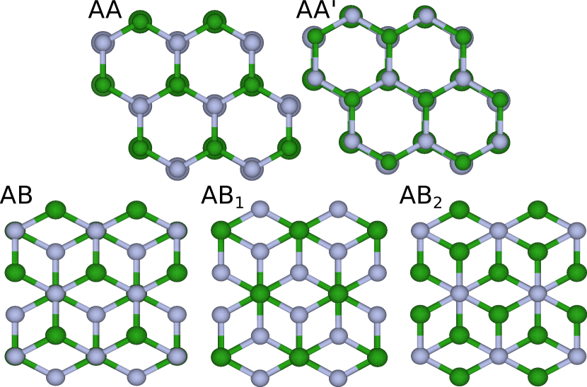
The analogy between monolayers can be extended to bilayers: surprisingly, their ground state geometries have practically the same interlayer distance, at least for the lowest energy stacking [33]. However, since both atoms of hBN are non-equivalent, there are more stacking possibilities [13]. The AA stacking of bilayer graphene is split in AA and AA’, as shown in Fig. 1. From simple electrostatic considerations, the AA’ has to be more stable than the AA stacking, since the closest interlayer neighbors have opposite charges.
Similarly, the Bernal stacking of graphene (AB) results in three possibilities, AB, AB1, AB2. Among the five possible stacking orders, three of them (AA’, AB, AB1) have practically the same binding energy, see Table 1. Two of the stacking possibilities, AA’ and AB, have been synthesized.[13]. The other arrangements could be obtained by the sliding of one of the layers,[14, 15, 16] or they can be found in inversion domains (local inversion of atomic positions) [34, 35, 36, 37].
| Stacking | (Å) | qB (e) | qN (e) | (meV) |
|---|---|---|---|---|
| AA | 3.53 | 0.21 | -0.21 | 25 (21[13], 40[38]) |
| AA’ | 3.34 | 0.21 | -0.21 | 0 (0[13], 0[38]) |
| AB | 3.36 | 0.21 | -0.21 | -3 (-2[13], 0[38]) |
| AB1 | 3.31 | 0.21 | -0.21 | -1 (2[13], 9[13]) |
| AB2 | 3.46 | 0.21 | -0.21 | 20 (18[13], 33[38]) |
The main properties of the bilayer are present in Table 1. The energies closely align with those reported in other studies [13, 39]. Particulary, the ground state corresponds to the AB structure instead of the AA’ stacking, usually found in real samples. The results are not so similar to calculations performed with wave functions methods[38]. Despite the high accuracy of these methods in molecules, it is not clear to the authors if this applies to vdW crystals. The only notable difference with the DFT-based literature is a lower energy of the AB1 relative to AA’ stacking. Our methodology for obtaining the total energy (HSE06) is expected to be more accurate than a PBE or vdW-corrected PBE scheme (see Sec. II for details). Nevertheless, this energy difference is less than 1 meV per atom and is not expected to be relevant for the SPEs.
The interlayer distance aligns with previous calculations without a van der Waals correction [39, 38]. Hirshfeld charges, indicative of the net charge at each atomic site, are independent of the stacking order. Therefore, the electrostatic potential exerted by one layer on the other depends solely on the local environment and interlayer distance. Throughout the remainder, unless explicitly stated otherwise, we will use an interlayer distance of 3.34Å (AA’ stacking, the most abundant one), isolating the effects on single photon emitters (SPEs).”
IV.2 Single photon emitters in the hBN bilayer
The groundstate energy levels of the defects C2 and C, for each stacking, are illustrated in Fig. 3, with other defects exhibiting a similar behavior. Compared to the hBN monolayer, the energy gap of the C2 levels consistently decreases in the bilayer, as expected from the enhanced screening. This effect in the C2 defect has been previously studied with more sophisticated methods [40], demonstrating a more pronounced impact when including many-body interactions. However, this enhancement of the screening in multilayers is not significantly larger than in the bilayer.
For non-adjacent defects as exemplified by C in Fig. 3B, the extra screening is less relevant, as expected due to the larger distance. Even in the energetically favorable stacking orders, there is practically no difference with the single layer. The previous trends hold true for all the defects studied here.
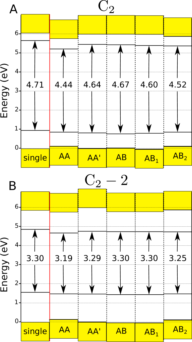
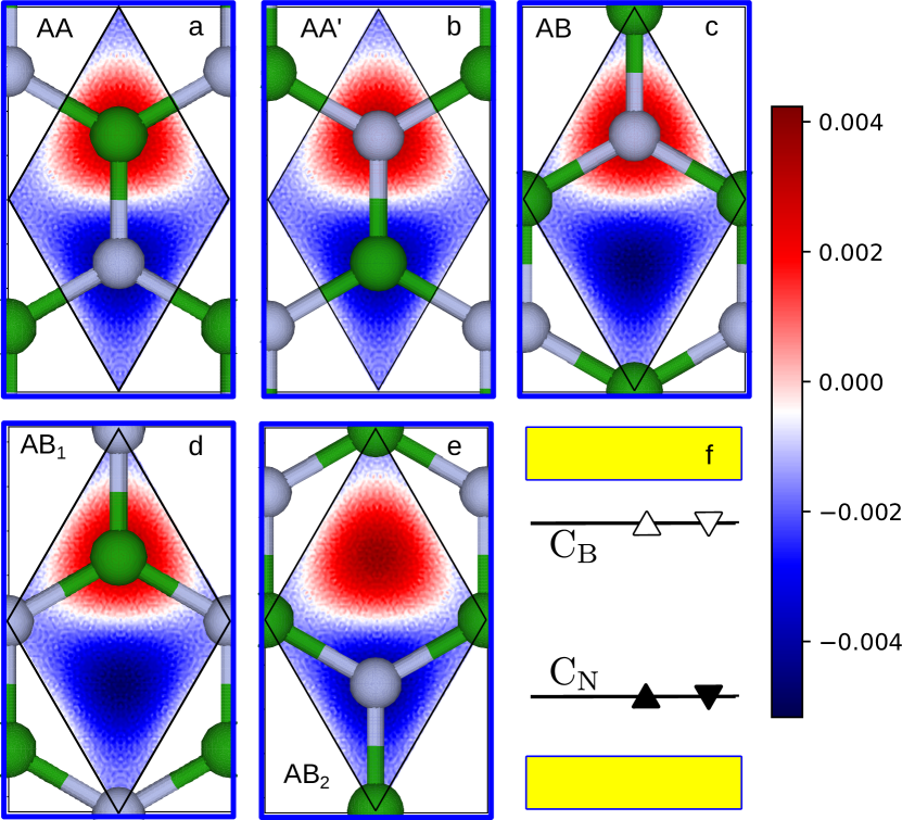
Different staking orders in the hBN bilayer result in variations in the energy gap, up to eV in the C2 defect, and eV in C2-2, see Fig. 3. Similar trends are observed for the remaining studied defects. The modulation of the gap with the stacking is readily understood with Eq. 7. For instance, take the AA’ stacking of as a reference structure. In this, the HOMO () lies in the region of positive potential while the LUMO () does in the region with the most negative potential (see panel b in Figure 2). In AA stacking, the situation is just the opposite (see panel a in Figure 2). Therefore, and , which implies, according to Eq. 7, that the gap of AA is smaller than the one of AA’. With similar arguments one would expect the gap of defects in all sackings of Figure 2 to be smaller than the gap of , which is the case except for . Interestingly, not only does the gap follow this predicted trend but the ZPL also does (see Table 2). Our model, however, has limitations, the main one we believe is that it does not include changes induced in the orbitals due to the second layer.
| Stacking | C2 | C | C | CN |
|---|---|---|---|---|
| AA | 3.82 | 2.95 | 2.62 | 2.37 |
| AA’ | 3.93 | 3.03 | 2.72 | 2.52 |
| AB | 3.96 | 3.05 | 2.71 | 2.59 |
| AB1 | 3.92 | 3.05 | 2.71 | 2.55 |
| AB2 | 3.88 | 3.00 | 2.67 | 2.37 |
| monolayer | 4.04 | 3.37 | 2.70 | 2.41 |
While the changes in the ZPL due to different stacking orders (Table 2) generally correlate with the alterations in the band gap, the degree of variation can be more or less pronounced for different defects. This is because, in the excited state, the occupations may not follow the simple donor-acceptor picture employed in our model. For instance, the defect CN has a groundstate with its HOMO localized on the C atom. However, its LUMO (occupied upon excitation) is mainly on the B atoms close to , with a node on the C atom. In other words, Eq. 7 provides a better approximation since have a minimal overlap. This induces a larger change in the ZPL due to different stacking orders, as shown in Table 2
On average, these changes in the ZPL are in the range of meV. For comparison, a ‘giant Stark effect’ measured in SPEs hosted in hBN is on the order of 30 meV [41]. The effect of the electrostatic potential due to different stacking in hBN bilayer can be tested by sliding one layer with respect to the other. Nevertheless, it could be much larger in van der Waals heterostructures formed by hBN plus another 2D material with an in-plane dipolar texture. Particularly, a 2D ferroelectric like In2Se3 could induce a substantial change in the ZPL controlled solely by a gate potential[42]. Such a study lies beyond the scope of this contribution, as other effects beyond screening and electrostatic take place.
V Conclusions
In this work, we explored the substrate effects on the electronic and optical properties of C-based in a 2D hBN. Our primary focus was on the effects of electrostatic interaction caused by the second pristine hBN layer. Using Janak’s theorem, we developed a simple perturbational model (Eq. 7) that captures the changes in the gap due to an external electrostatic perturbation. The advantage of utilizing the electrostatic potential of a substrate is that the microscopic fields are much larger than the static field produced by electrodes for instance, which results in larger modulations of the gap. For instance, the modulation via the ‘giant Stark effect’ in similar systems is about 30 meV. In our study, we observed changes up to 100 meV for the C defect, and over 200 meV for the CN defect.
Our results provide insight into the impact of the substrate on the properties of quantum defects and show that if we could control the location of the defects in suitable areas of the electrostatic potential generated by the substrate, one could modulate the optical properties of this type of defects. This presents an alternative strategy to conventional methods such as strain modulation of 2D materials or the design of van der Waals heterostructures with other insulating materials.
Acknowledgements.
We Acknowledge financial support by FONDECYT through grants 1220366, 1231487, 1220715 and by Center for the Development of Nanosciences and Nanotechnology, CEDENNA AFB 220001. FM is supported by Conicyt PIA/Anillo ACT192023 W.M. Acknowledges the support of ANID Chile through the Doctoral National Scholarship N. J.C acknowledges the support of ANID Chile through the Doctoral National Scholarship N Powered@NLHPC: This research was partially supported by the supercomputing infrastructure of the NLHPC (ECM-02).References
- White et al. [2021] S. J. U. White, T. Yang, N. Dontschuk, C. Li, Z.-Q. Xu, M. Kianinia, A. Stacey, M. Toth, and I. Aharonovich, Electrical control of quantum emitters in a van der waals heterostructure (2021).
- Kianinia et al. [2020] M. Kianinia, S. White, J. E. Fröch, C. Bradac, and I. Aharonovich, Generation of spin defects in hexagonal boron nitride, ACS Photonics 7, 2147 (2020).
- Gao et al. [2021] X. Gao, S. Pandey, M. Kianinia, J. Ahn, P. Ju, I. Aharonovich, N. Shivaram, and T. Li, Femtosecond laser writing of spin defects in hexagonal boron nitride, ACS Photonics 8, 994 (2021).
- Mendelson et al. [2021] N. Mendelson, D. Chugh, J. R. Reimers, T. S. Cheng, A. Gottscholl, H. Long, C. J. Mellor, A. Zettl, V. Dyakonov, P. H. Beton, et al., Identifying carbon as the source of visible single-photon emission from hexagonal boron nitride, Nature materials 20, 321 (2021).
- Auburger and Gali [2021] P. Auburger and A. Gali, Towards ab initio identification of paramagnetic substitutional carbon defects in hexagonal boron nitride acting as quantum bits, Phys. Rev. B 104, 075410 (2021).
- Jara et al. [2021] C. Jara, T. Rauch, S. Botti, M. A. L. Marques, A. Norambuena, R. Coto, J. E. Castellanos-Águila, J. R. Maze, and F. Munoz, First-principles identification of single photon emitters based on carbon clusters in hexagonal boron nitride, J. P. Chem. A 125, 1325 (2021).
- Du et al. [2015] X. Z. Du, J. Li, J. Y. Lin, and H. X. Jiang, The origin of deep-level impurity transitions in hexagonal boron nitride, Applied Physics Letters 106, 021110 (2015).
- Mackoit-Sinkeviciene et al. [2019] M. Mackoit-Sinkeviciene, M. Maciaszek, C. G. Van de Walle, and A. Alkauskas, Carbon dimer defect as a source of the 4.1 ev luminescence in hexagonal boron nitride, Applied Physics Letters 115, 212101 (2019).
- Li et al. [2022a] S. Li, A. Pershin, G. Thiering, P. Udvarhelyi, and A. Gali, Ultraviolet quantum emitters in hexagonal boron nitride from carbon clusters, The Journal of Physical Chemistry Letters 13, 3150 (2022a).
- Li et al. [2022b] K. Li, T. J. Smart, and Y. Ping, Carbon trimer as a 2 ev single-photon emitter candidate in hexagonal boron nitride: A first-principles study, Phys. Rev. Materials 6, L042201 (2022b).
- Pinilla et al. [2022] F. Pinilla, N. Vasquez, J. R. Maze, C. Cárdenas, and F. Munoz, Carbon-based single photon emitters in hexagonal boron nitride with triplet ground state (2022), arXiv:2209.13735 [cond-mat.mtrl-sci] .
- Maciaszek et al. [2022] M. Maciaszek, L. Razinkovas, and A. Alkauskas, Thermodynamics of carbon point defects in hexagonal boron nitride, Phys. Rev. Materials 6, 014005 (2022).
- Gilbert et al. [2019] S. M. Gilbert, T. Pham, M. Dogan, S. Oh, B. Shevitski, G. Schumm, S. Liu, P. Ercius, S. Aloni, M. L. Cohen, and A. Zettl, Alternative stacking sequences in hexagonal boron nitride, 2D Materials 6, 021006 (2019).
- Yasuda et al. [2021] K. Yasuda, X. Wang, K. Watanabe, T. Taniguchi, and P. Jarillo-Herrero, Stacking-engineered ferroelectricity in bilayer boron nitride, Science 372, 1458 (2021).
- Stern et al. [2021] M. V. Stern, Y. Waschitz, W. Cao, I. Nevo, K. Watanabe, T. Taniguchi, E. Sela, M. Urbakh, O. Hod, and M. B. Shalom, Interfacial ferroelectricity by van der waals sliding, Science 372, 1462 (2021).
- Jiang et al. [2022] W. Jiang, C. Liu, X. Ma, X. Yu, S. Hu, X. Li, L. A. Burton, Y. Liu, Y. Chen, P. Guo, X. Kong, L. Bellaiche, and W. Ren, Anomalous ferroelectricity and double-negative effects in bilayer hexagonal boron nitride, Phys. Rev. B 106, 054104 (2022).
- Kresse and Hafner [1993] G. Kresse and J. Hafner, Ab initio molecular dynamics for liquid metals, Phys. Rev. B 47, 558(R) (1993).
- Kresse and Hafner [1994] G. Kresse and J. Hafner, Ab initio molecular-dynamics simulation of the liquid-metal–amorphous-semiconductor transition in germanium, Phys. Rev. B 49, 14251 (1994).
- Kresse and Furthmüller [1996] G. Kresse and J. Furthmüller, Efficiency of ab-initio total energy calculations for metals and semiconductors using a plane-wave basis set, Comput. Mater. Sci. 6, 15 (1996).
- Kresse and Furthmüller [1996] G. Kresse and J. Furthmüller, Efficient iterative schemes for ab initio total-energy calculations using a plane-wave basis set, Phys. Rev. B 54, 11169 (1996).
- Perdew et al. [1996] J. P. Perdew, K. Burke, and M. Ernzerhof, Generalized gradient approximation made simple, Phys. Rev. Lett. 77, 3865 (1996).
- Heyd et al. [2003] J. Heyd, G. E. Scuseria, and M. Ernzerhof, Hybrid functionals based on a screened coulomb potential, J. Chem. Phys. 118, 8207 (2003).
- Krukau et al. [2006] A. V. Krukau, O. A. Vydrov, A. F. Izmaylov, and G. E. Scuseria, Influence of the exchange screening parameter on the performance of screened hybrid functionals, J. Chem. Phys. 125, 224106 (2006).
- Tkatchenko and Scheffler [2009] A. Tkatchenko and M. Scheffler, Accurate molecular van der waals interactions from ground-state electron density and free-atom reference data, Phys. Rev. Lett. 102, 073005 (2009).
- Jin et al. [2021] Y. Jin, M. Govoni, G. Wolfowicz, S. E. Sullivan, F. J. Heremans, D. D. Awschalom, and G. Galli, Photoluminescence spectra of point defects in semiconductors: Validation of first-principles calculations, Phys. Rev. Materials 5, 084603 (2021).
- Kresse and Joubert [1999] G. Kresse and D. Joubert, From ultrasoft pseudopotentials to the projector augmented-wave method, Phys. Rev. B 59, 1758 (1999).
- Herath et al. [2019] U. Herath, P. Tavadze, X. He, E. Bousquet, S. Singh, F. Muñoz, and A. H. Romero, Pyprocar: A python library for electronic structure pre/post-processing, Comput. Phys. Commun. 251, 107080 (2019).
- Momma and Izumi [2011] K. Momma and F. Izumi, Vesta 3 for three-dimensional visualization of crystal, volumetric and morphology data, Journal of applied crystallography 44, 1272 (2011).
- Geerlings et al. [2003] P. Geerlings, F. De Proft, and W. Langenaeker, Conceptual density functional theory, Chemical reviews 103, 1793 (2003).
- Fuentealba and Cárdenas [2013] P. Fuentealba and C. Cárdenas, On the exponential model for energy with respect to number of electrons, Journal of molecular modeling 19, 2849 (2013).
- Janak [1978] J. F. Janak, Proof that in density-functional theory, Phys. Rev. B 18, 7165 (1978).
- Cerón et al. [2020] M. L. Cerón, T. Gomez, M. Calatayud, and C. Cárdenas, Computing the fukui function in solid-state chemistry: Application to alkaline earth oxides bulk and surfaces, The Journal of Physical Chemistry A 124, 2826 (2020).
- Hod [2012] O. Hod, Graphite and hexagonal boron-nitride have the same interlayer distance. why?, Journal of Chemical Theory and Computation 8, 1360 (2012).
- Cretu et al. [2014] O. Cretu, Y.-C. Lin, and K. Suenaga, Evidence for active atomic defects in monolayer hexagonal boron nitride: A new mechanism of plasticity in two-dimensional materials, Nano Letters 14, 1064 (2014).
- Li et al. [2015] Q. Li, X. Zou, M. Liu, J. Sun, Y. Gao, Y. Qi, X. Zhou, B. I. Yakobson, Y. Zhang, and Z. Liu, Grain boundary structures and electronic properties of hexagonal boron nitride on cu(111), Nano Letters 15, 5804 (2015).
- Liu et al. [2012] Y. Liu, X. Zou, and B. I. Yakobson, Dislocations and grain boundaries in two-dimensional boron nitride, ACS Nano 6, 7053 (2012).
- Taha et al. [2017] D. Taha, S. K. Mkhonta, K. R. Elder, and Z.-F. Huang, Grain boundary structures and collective dynamics of inversion domains in binary two-dimensional materials, Phys. Rev. Lett. 118, 255501 (2017).
- Constantinescu et al. [2013] G. Constantinescu, A. Kuc, and T. Heine, Stacking in bulk and bilayer hexagonal boron nitride, Phys. Rev. Lett. 111, 036104 (2013).
- Ribeiro and Peres [2011] R. M. Ribeiro and N. M. R. Peres, Stability of boron nitride bilayers: Ground-state energies, interlayer distances, and tight-binding description, Phys. Rev. B 83, 235312 (2011).
- Amblard et al. [2022] D. Amblard, G. D’Avino, I. Duchemin, and X. Blase, Universal polarization energies for defects in monolayer, surface, and bulk hexagonal boron nitride: A finite-size fragments approach, Phys. Rev. Mater. 6, 064008 (2022).
- Noh et al. [2018] G. Noh, D. Choi, J.-H. Kim, D.-G. Im, Y.-H. Kim, H. Seo, and J. Lee, Stark tuning of single-photon emitters in hexagonal boron nitride, Nano Letters 18, 4710 (2018), pMID: 29932664.
- Ding et al. [2017] W. Ding, J. Zhu, Z. Wang, Y. Gao, D. Xiao, Y. Gu, Z. Zhang, and W. Zhu, Prediction of intrinsic two-dimensional ferroelectrics in in2se3 and other iii2-vi3 van der waals materials, Nature communications 8, 14956 (2017).