Colossal Magnetoresistance in Twisted Intertwined Graphene Spirals
Abstract
Colossal magnetoresistance (CMR) is highly applicable in spintronic devices such as magnetic sensors, magnetic memory, and hard drives. Typically, CMR is found in Weyl semimetals characterized by perfect electron-hole symmetry or exceptionally high electric conductivity and mobility. Our study explores this phenomenon in a recently developed graphene moir system, which demonstrates CMR owing to its topological structure and high-quality crystal formation. We specifically investigate the electronic properties of three-dimensional (3D) intertwined twisted graphene spirals (TGS), manipulating the screw dislocation axis to achieve a rotation angle of 7.3∘. Notably, at 14 T and 2 K, the magnetoresistance of these structures reached 1.7107%, accompanied by an unexpected metal-to-insulator transition as the temperature increased. This transition becomes noticeable when the magnetic field exceeds a minimal threshold of approximately 0.1 T. These observations suggest the existence of complex, correlated states within the partially filled three-dimensional Landau levels of the 3D TGS system. Our findings open up new possibilities for achieving CMR by engineering the topological structure of 2D layered moir systems.
I INTRODUCTION
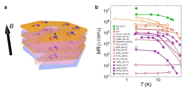
Giant magnetoresistance (GMR), typically below 100 percent, is common in thin-film metals and manganese-based perovskite, playing a crucial role in spintronic devices[1, 2]. The demand for higher performance has led to a focus on colossal magnetoresistance (CMR), characterized by a substantial increase in resistivity under magnetic fields, without saturation even at very high fields and low temperatures[3, 4, 5, 6, 7, 8, 9]. This CMR, fundamentally distinct from GMR, is often observed in semimetals with topological properties and balanced electron-hole carriers as collected in Fig. 1b[3].
Notably, van der Waals semimetals like WTe2[4], MoTe2[5, 6], and NbSb2[7] display CMR (1105% at 2 K). Angle-resolved photoemission spectroscopy (ARPES) studies in these materials reveal electron and hole Fermi surfaces of equal size[8], indicating a resonant compensated semimetal nature. Similarly, the 3D transition metal diphosphides, WP2 and MoP2, showcase promising CMR due to closely neighboring Weyl points. Other semimetals like LaSb[9], TaAs[10, 11], NbP[12], Cd3As[13], and PtSn4[14] also exhibit CMR, mainly due to nearly perfect electron-hole compensation or high conductivity and mobility.
Graphite, a fundamental semimetal, has shown impressive CMR progress, attributed to its topological defects such as stacking faults, and sample quality[15]. In twisted graphene/boron–nitride (BN) heterostructure[16], magnetoresistance (MR) values reach 880% at 400 K (9 T). A CMR of 110% at 300 K (0.1 T) was reported in twisted BN/graphene/BN, linked to Dirac plasma in the moir system[17]. A record MR value of 1107% (21 T) in micrometer-sized natural graphite suggests the importance of moir patterns in CMR. The 2018 discovery of superconductivity in magic-angle twisted bilayer graphene marked a milestone[18, 19], making moir superlattices a key focus in condensed matter physics[20, 21, 22, 23, 24]. These layers exhibit unique phenomena due to the interplay between graphene’s Dirac wavefunctions and the interlayer moir potential[25, 26, 27, 28], leading to flat bands with nontrivial topology[21, 29, 30, 31, 32, 33, 34, 35, 36]. Recently, a three-dimensional bulk moir graphite superlattice, consisting of alternating twisted graphene layers, was synthesized[37]. This structure, theoretically capable of ’magic momenta’ and 3D Landau levels[38], may be a new platform for studying correlated and topological physics.
Our study explores the transport properties of this new bulk moir graphite, comprising hundreds and thousands of alternating twisted graphene multilayers, stacked along a spiral dislocation, as schematically shown in Fig. 1(a). The twisted graphene spirals (TGS) exhibit extremely high carrier mobility ( = 3106 cm2V-1s-1), forming Landau levels under low magnetic fields (0.1 T). We observed a colossal magnetoresistance of 1.7107% at 2 K under a 14 T magnetic field in this 3D TGS system.
II Result and Disscusion
II.1 Colossal magnetoresistance
In Fig. 1b we present the temperature dependent MRs (at B= 7 T) of several typical high-MR materials including Weyl semimetals[4, 5, 6, 8, 9, 10, 39], Dirac semimetals[7, 13, 14, 40], nodal-line semimetals[41] (according to the degeneracy and momentum space distribution of the nodal points), NG and HOPG[15, 42], graphene[16, 43], and twisted spiral graphene presented in this work. Clearly twisted spiral graphene holds the record-high MR in this moderate magnetic-field regime. The MR at T = 2 K and B = 7 T is up to about 5106%, which is a record high value among all MRs measured at moderate magnetic fields (<10 T) reported in literatures. The value of MR in another sample reaches 1.7107% with applied field B = 14 T at T = 2 K. For large MR, various potential mechanisms have been proposed, including electron-hole compensation, steep band, ultrahigh mobility, high residual resistivity ratio (RRR), topological fermions, etc. Mechanisms mentioned above can be analyzed through quantum oscillation and Hall effect measurement. Furthermore, a large MR is correlated with other systems, such as 2D materials, which carriers are limited to the 2D plane and the electronic structure largely depended on the thickness of material. However, the MR of the highly oriented pyrolytic graphite (HOPG) reveals MR of only about 1101% [15, 42, 43, 44], being several orders of magnitudes smaller than that of the bulk twisted GS. Nevertheless, an extremely high MR of about1106% (2 K, 7 T) has also observed in the Sri Lankan natural graphite (NG), for which the existence of highly conducting 2D interfaces aligned parallel to the graphene planes are attributed to the origin[15, 42, 43, 44].
Another system concentrated here is topological materials, which are characterized by symmetry protected band crossing at or near the Fermi level in the Brillouin zone. Particularly, the present record of the maximum MR was reported in type-II Weyl semimetal WP2 (2106%, 7 T, 2 K)[39]. Such spectacularly large MR in WP2 were attributed to both the nontrivial wavefunction textures around Weyl nodes and the presence of compensating electron and hole pockets in the Fermi surface, where the former can suppress back scatterings and induce considerably large mobilities[12, 39, 13, 45].As reported in nature graphite U11[15], the large MR in graphite shares different origin from Weyl semimetals. Due to the advanced growth method proliferates the scope of graphene moir superlattices[37], bulk graphite comprises alternatingly twisted graphene multilayers, which are sequentially stacked along a spiral dislocation. While the topological structure of GS still deserves discussion and the structure of the GS will be introduced at the following section.
II.2 Structure of the twisted graphene spira
In the scanning electron microscopy (SEM) imaging, we observe stepwise variations in contrast, allowing us to discern up to ten individual graphene layers [46]. Given that each graphene spiral (GS) in crystal is comprised of several dozen turns, SEM thus is not adept at distinguishing the contours of GS with up to ten layers. To circumvent this limitation, we resort to confocal laser scanning microscopy (CLSM), which possesses the ability to simultaneously generate intensity and topographical images. This facilitates the measurement of the in-plane dimensions and the out-of-plane stacking sequence of the as-grown GSs [47]. Through CLSM, we confirm that the chemical vapor deposition (CVD) approach is proficient at producing GSs with dimensions spanning hundreds of micrometers, revealing interlayers characterized by an approximate twist angle of 7∘ (as showcased in Figure 2a and Fig. S8). Additionally, the adjacent zigzag edges of these spirals tilt at an angle of 7∘, a detail captured in the atomic force microscopy (AFM) imagery presented in Fig. S8. Such evidence intimates that the freshly synthesized GSs adopt an intertwined helical configuration, characterized by a twist of 7∘.
To further validate the presence of an intertwined helical structure with a homogeneous twist angle, we transferred the identical GS onto a transmission electron microscopy (TEM) grid for TEM diffraction measurements, following the transport measurements (which will be discussed later). The TEM observations, along with the corresponding selected area electron diffraction (SAED) patterns, reveal that the twist angle of the GS is 7.30.176∘ (Fig. 2b and Fig. S8). Significantly, the twist angle determined through SAED is consistent with the findings from CLSM and AFM observations in Fig. 2a and Fig. S8. More accurate twist angle measurements were made by diffraction mode of TEM, which allowing for the observation of superlattices formed by a pair of graphene lattices in the diffraction pattern, as depicted in Fig. 2b top inset. It is worth mentioning that electron diffraction of moir patterns can also be observed, exhibiting the same symmetry as the original lattice.
The relative rotation of the GS leads to the formation of a periodic moir superlattice within the helical graphene structure. The wavelength of this superlattice () is determined by the twisted angle () present in the moir superlattice, =/(2sin(/2)) (: the lattice constant of the monolayer graphene)[48]. High-resolution TEM characterization reveals the presence of a moir pattern with a twist angle of = 7.3∘, corresponding to a superlattice wavelength of approximately 1.93 nm. Fig. 2c clearly shows the moir pattern as a periodic arrangement of bright and dark regions, with a wavelength of approximately 1.93 nm, confirming that it corresponds to the twist angle of 7.3∘. Based on these comprehensive characterizations, we conclude that the as-grown GSs consist of intertwined helical structures with a 7∘ in-plane twist, as depicted in the schematic illustrations in Fig. 2d.
To obtain a precise characterization of the out-of-plane structure of the GS and further confirm the presence of intertwined helical structures, cross-sectional TEM samples were prepared. These samples were extracted from the identical GS after performing CLSM observations (Fig. S6), TEM measurements (Fig. 2b), and magnetoresistance measurements (Fig. 1 and 3). The site-specific focused ion beam (FIB) lift-out technique was employed to prepare the GS cross-sectional samples. The process of FIB preparation for observing the cross-sectional structure of the GS is depicted in Supplementary Information Fig. S6.
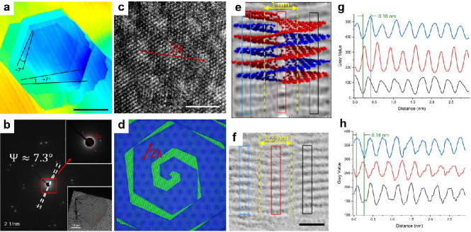
The cross-sectional scanning transmission electron microscopy (STEM) observations (Fig. S7) reveal a double staggered series of graphene planes, suggesting the presence of a screw dislocation with a double helical structure. In order to gain a better understanding of the cross-sectional structure of the screw dislocation in the graphene multilayers, we constructed a structural model for the double helical structure which is further relaxed using molecular dynamics simulations. Then, we perform STEM intensity simulations based on the fully relaxed double helical structure using QSTEM code package [49]. Fig. 2e presents a schematic model of the double helical structure of GS, accompanied by simulated STEM images derived from the fully relaxed structural model. Figs. 2e-h present a comparison between the configuration of the simulated double helical structure and the experimentally observed images (Figs. 2e, f). While the atomic structure cannot be completely determined from the cross-sectional STEM image, the stacking configuration and curvature closely resemble the expected double helical structure. This can be visualized as a result of cutting through the -bonded graphene layers perpendicularly, causing them to slip along the cutting line by two layers and reconnecting the bonds. Line profiles were plotted perpendicular to the lateral graphene layers, highlighting the distinctive configuration with double staggered graphene planes (Figs. 2g, h). This configuration involves a helical path traced around the linear defect (spiral core) as the atomic planes slip within the crystalline lattice. Indeed, a comparison of the line profile between the simulated double helical structure and the experimental observation reveals a remarkable similarity. This similarity is characterized by an integral-sliding pattern within the spiral core, where the atomic planes exhibit a shift equivalent to half a lattice of carbon layers. The line profile analysis clearly shows a shift in the layered stacking configuration of approximately 0.18 nm (half the interlayer spacing of graphite) within the spiral core region (highlighted by the red stripes in Figs. 2e, f), compared to the surrounding areas (blue and black stripes). The remarkable consistency between the experimental line profile of the cross-sectional GS and the simulated image further confirms the proposed double helical structure.
II.3 Quantum oscillation
As well studied in previous works, a twist angle between two adjacent graphene layers can fundamentally change their electronic band structures, leading to topological flat bands which are responsible for various novel phenomena in electronic transport properties. The transport properties of the bulk twisted GS were investigated in a conventional four-terminal methods, and magnetic fields were applied parallel to the -axis. The natural graphite (NG) was also studied as a comparison. A typical low temperature data for in-plane longitudinal resistivity () of twisted GS as a function of the magnetic field from = 0-9 T is shown in Fig. 3a. increases colossally with the magnetic field, and, at 9 T, it is almost 7 orders of magnitude larger than the zero-field value, which will be analyzed in next section. In addition, Shubnikov-de Haas (SdH) oscillations are superimposed on the large magnetoresistance background. These oscillations, which start at a low magnetic field 0.1 T, can be better observed in the background-removed data plotted in Figure 2a and b. The background can be removed by subtracting a smoothed data curve. Fig. 3b shows oscillations under a smaller magnetic field region at different temperatures from 2 K to 16 K. Two series of oscillations can be distinguished. In the Fourier transformation of the versus (1/) data shown in Fig. 3b inset, two frequencies are founded and assigned to electron pocket (4.67 T) and hole pocket (6.67 T). Peaks , correspond to the 1st and 2nd harmonics of oscillations from electrons and holes. Thus, the area of fermi surface ( for electrons and for holes) can be obtained throw the function , where is the FFT frequency, is reduced Planck’s constant, is elementary charge, is area of Fermi surface. Carrier mobility and concentration can reflect quasi-particle properties near the Fermi level, which are two important parameters of a material that can be derived from the Hall coefficient.
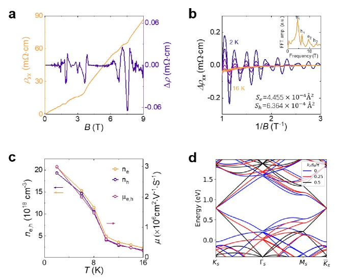
Hall effect measurements have been performed in field sweep mode. The field dependence of the Hall resistivity () exhibits a nonlinear behavior in low fields indicates the involvement of more than one type of charge carrier in the transport properties. The nonlinear Hall curve may be described by the two-carrier model [50]:
| (1) |
where () and are the carrier density and mobility of electrons (holes), respectively. The mobilities of electron-type and hole-type are assumed to be equal at low temperatures, as both of them are quasi-particle excitations around the Dirac points which have similar scattering mechanisms. The fitting result can be seen in Figure 2c. The electron (hole) carrier concentration is found to be cm-3 ( cm-3) at 2 K, with a net electron carrier concentration =1.41018 cm-3. The corresponding mobility exhibits a high value cm2 V-1 s-1. This value is close to that of the Weyl semimetal NbP (5106 cm2 V-1 s-1) [12].The quantum oscillation behavior may be qualitatively understood from the low-energy band structures of the bulk twisted intertwined GS. Away from the central dislocation core, the system can be viewed as numerous layers of TBG which are coupled via nearest neighbor interlayer hopping. As a result, such bulk moir superlattice is bestowed an additional vertical wavevector () degree of freedom. When the twist angle is relatively large (), the low-energy band structure consists of Dirac cones in the - plane, with -renormalized Fermi velocities, as shown in Fig. 2(d). Neglecting the frame-rotation effects of the two graphene layers, it turns out that the low-energy states of the system have an approximate particle-hole symmetry at each vertical wavevector . Consequently, the Dirac point at each is pinned to the same energy by virtue of this particle-hole symmetry. Including the frame-rotation effects would shift the energy of the Dirac point, leading to a dispersion of the form [51], with 3.5 meV, leading to a dispersion of Dirac points 7 meV. This may lead to co-existence of electron and hole carriers even when the system is charge neutral. Moreover, other effects such as the variation of the interlayer distance (from 3.35 angstrom to 3.50 angstrom according to the TEM measurements) and remote-band renormalization effects may further enhance the dispersion of the Dirac points, which qualitatively explains the co-existing electron- and hole-type carriers in the system. As a two-band system with similar carrier concentration between electrons and holes, compensation mechanism can be a major factor. Considering the effect of topological Landau levels on MR, we measured () curves under different magnetic field.
II.4 Anomalous metal-insulator transition
Fig. 4a shows the temperature dependence of normalized of twisted GS and NG under zero magnetic field. The twisted GS shows a much larger residual resistivity ratio (RRR) [(300 K)/(2 K)] = 38, which is considerably larger than that of NG (RRR = 6). Generally, the less residual resistivity demonstrates high-quality of single crystals with less impurity scattering. However, the special lattice structure of the bulk twisted GS may also induce significant resistivity difference due to the dramatic changes in the band structures, as has been observed in twisted bilayer graphene [52, 53].
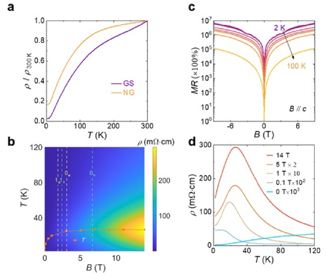
A color map of resistivity in the plane of the temperature from 2 to 120 K and magnetic field from 0 to 14 T has been shown in Fig. 4b. An unconventional transition from metallic behavior (where resistivity increases with temperature) to insulator-like behavior (where resistivity decreases with temperature) appears when a finite external magnetic field has been applied. Transition temperature has been defined where = 0. The orange scatterline shows the field dependence of . As the magnetic field increases, the rises rapidly and finally saturates to 26.9 K when the field is larger than 3 T. This is exactly the same magnetic field value above which the zeroth landau level starts to be filled, as marked by the rightmost yellow dashed line in Fig. 4b. Line cuts of resistivity versus temperature for several typical values of magnetic fields varying from 0 to 14 T can be seen in Fig. 4d. A monotonic temperature dependence where increases with temperature has been observed under zero magnetic field; and a nonzero 2 K emerges when the field is increased to 0.1 T, which is the same characteristic field amplitude for the onset of Landau level quantization. This implies that the anomalous metal-to-insulator transition at temperature may be attributed to the correlation effects of the electrons in partially occupied Landau levels. Especially, in such bulk twisted GS system the linear Dirac dispersions and the quasi-2D Fermi surface would lead to weakly dispersive higher Landau levels and even dispersionless zeroth Landau level in such a 3D bulk system, which may significantly boost electron-electron interaction effects.
Line profiles of MRs under different temperatures are presented in Fig. 4c. This colossal magnetoresistance is concomitant with an anomalous metal-to-insulator transition with increasing temperature, which is reminiscent of isospin Pomeranchuck effect observed in magic-angle twisted bilayer graphene[54, 55]. A temperature dependence of MR under magnetic field ranging from 3 T to 14 T (shown in Fig. S3) exhibits an ultrahigh MR reaching 3.4104% under 14 T even at room temperature 300 K. Undisputedly, the topological dispresionless Landau level in such large-angle-twisted GS have enhanced the MR under a high magnetic field, although the specific mechanism still deserves further research.
III Conclusion
In conclusion, our work has revealed a CMR and a remarkable metal-to-insulator transition in a bulk graphite superlattice arranged in a 3D TGS system. Through quantum oscillation measurements, we identified two distinct frequencies that correspond to separate charge carrier pockets: an electron pocket at 4.67 T and a hole pocket at 6.67 T. These findings are corroborated by Hall effect measurements. The simultaneous presence of both electron-type and hole-type carriers suggests a disruption in the particle-hole symmetries, possibly influenced by variations in the interlayer spacing and remote-band renormalization effects.
Upon applying an external magnetic field, we observed a notable transition from metallic to insulator-like behavior. The critical temperature, , stabilizes around 26.9 K in fields above 3 T, indicating the onset of filling in the 3D zeroth Landau level. This behavior implies that the transition may stem from correlation effects among electrons in these partially filled 3D Landau levels. Accompanying this transition is a colossal magnetoresistance, measured at approximately 1.7107% at 2 K and 14 T, setting a new record. This significant increase in magnetoresistance is linked with the metal-to-insulator transition and is reminiscent of the isospin Pomeranchuck effect observed in magic-angle twisted bilayer graphene.
Our results establish the TGS as a potential new platform for studying CMR in 2D layered materials, alongside correlated and topological phenomena typically observed in moiré graphite superlattices.
IV Methods
Structure analysis.Transmission electron microscopy analysis. The Polymethyl Methacrylate (PMMA) solution was spin-coated onto the GS crystal at a speed of 600 rounds per minute (rpm) for 5 s, followed by spinning at a speed of 3000 rpm for 60 s and then drying at room temperature for 10 min. Following the drying process, the prepared sample was transferred onto a gold grid, and the PMMA protective layer was removed through a soaking procedure in acetone. Subsequently, Aberration-corrected transmission electron microscopy was carried out using a JEOL Grand Arm 300F, operated at 80 kV to minimize the risk of inducing knock-on damage to graphene. Image acquisition was performed with exposure time of 0.5 s on a OneView camera binned to pixel resolution. Post-processing of acquired images was undertaken for further analysis and enhancement of data quality.
Theoretical analysis. The structural relaxation is calculated utilizing Large-scale Atomic-Molecular Massively Parallel Simulation (LAMMPS)[56] with long-rang bond-order potential for carbon (LCBOP) [57]. A moir supercell with periodic boundary condition applied in both the in-plane and out-of-plane directions, serves as the initial lattice structure. The twist angles between two layers, in accordance with the commensurate condition, are 7.34∘. The steepest descent algorithm is employed in the lattice relaxation calculations. The calculation of the band structure of twisted GS is performed utilizing the tight-binding (TB) model [58] based on the full relaxed structure. To be specific, the hopping amplitude between two orbitals at different sites is expressed as:
| (2) |
where and is the displacement vector between two sites. = 3.44 Å is the interlayer distance. =1.42 Å is the distance between two nearest neighbor carbon atoms. = 0.184. = 0.48 eV and = -2.7 eV.
V Acknowledgements
This research was supported in part by the Ministry of Science and Technology (MOST) of China (Nos. 2022YFA1603903 and 2020YFA0309601), the National Natural Science Foundation of China (Grants Nos. 12174257, 12004251, 12104302, 12104303, 12304217), the Natural Science Foundation of Shanghai (Grant No. 20ZR1436100), the Science and Technology Commission of Shanghai Municipality (Grant No. 21JC1405100), the Shanghai Sailing Program (Grant No. 21YF1429200), the start-up funding from ShanghaiTech University, and Beijing National Laboratory for Condensed Matter Physics, the Interdisciplinary Program of Wuhan National High Magnetic Field Center (WHMFC202124).
References
- Baibich et al. [1988] M. N. Baibich, J. M. Broto, A. Fert, F. N. Van Dau, F. Petroff, P. Etienne, G. Creuzet, A. Friederich, and J. Chazelas, Giant magnetoresistance of (001)fe/(001)cr magnetic superlattices, Physical Review Letters 61, 2472 (1988), pRL.
- Binasch et al. [1989] G. Binasch, P. Grünberg, F. Saurenbach, and W. Zinn, Enhanced magnetoresistance in layered magnetic structures with antiferromagnetic interlayer exchange, Physical Review B 39, 4828 (1989), pRB.
- Hasan et al. [2021] M. Z. Hasan, G. Chang, I. Belopolski, G. Bian, S.-Y. Xu, and J.-X. Yin, Weyl, dirac and high-fold chiral fermions in topological quantum matter, Nature Reviews Materials 6, 784 (2021).
- Ali et al. [2014] M. N. Ali, J. Xiong, S. Flynn, J. Tao, Q. D. Gibson, L. M. Schoop, T. Liang, N. Haldolaarachchige, M. Hirschberger, N. P. Ong, and R. J. Cava, Large, non-saturating magnetoresistance in WTe2, Nature 514, 205 (2014).
- Lee et al. [2018a] S. Lee, J. Jang, S.-I. Kim, S.-G. Jung, J. Kim, S. Cho, S. W. Kim, J. Y. Rhee, K.-S. Park, and T. Park, Origin of extremely large magnetoresistance in the candidate type-II Weyl semimetal MoTe2-x, Scientific Reports 8, 10.1038/s41598-018-32387-1 (2018a).
- Chen et al. [2016] F. C. Chen, H. Y. Lv, X. Luo, W. J. Lu, Q. L. Pei, G. T. Lin, Y. Y. Han, X. B. Zhu, W. H. Song, and Y. P. Sun, Extremely large magnetoresistance in the type-II Weyl semimetal MoTe2, Physical Review B 94, 10.1103/PhysRevB.94.235154 (2016).
- Wang et al. [2014] K. Wang, D. Graf, L. Li, L. Wang, and C. Petrovic, Anisotropic giant magnetoresistance in NbSb2, Scientific Reports 4, 10.1038/srep07328 (2014).
- Pletikosi et al. [2014] I. Pletikosi, M. N. Ali, A. . Fedorov, R. . Cava, and T. Valla, Electronic Structure Basis for the Extraordinary Magnetoresistance in WTe2, Physical Review Letters 113, 10.1103/PhysRevLett.113.216601 (2014).
- Tafti et al. [2015] F. F. Tafti, Q. D. Gibson, S. K. Kushwaha, N. Haldolaarachchige, and R. J. Cava, Resistivity plateau and extreme magnetoresistance in LaSb, Nature Physics 12, 272 (2015).
- Yuan et al. [2016] Z. Yuan, H. Lu, Y. Liu, J. Wang, and S. Jia, Large magnetoresistance in compensated semimetals TaAs2 and NbAs2, Physical Review B 93, 10.1103/PhysRevB.93.184405 (2016).
- Luo et al. [2016] Y. Luo, R. D. McDonald, P. F. S. Rosa, B. Scott, N. Wakeham, N. J. Ghimire, E. D. Bauer, J. D. Thompson, and F. Ronning, Anomalous electronic structure and magnetoresistance in TaAs2, Scientific Reports 6, 10.1038/srep27294 (2016).
- Shekhar et al. [2015] C. Shekhar, A. K. Nayak, Y. Sun, M. Schmidt, M. Nicklas, I. Leermakers, U. Zeitler, Y. Skourski, J. Wosnitza, Z. Liu, Y. Chen, W. Schnelle, H. Borrmann, Y. Grin, C. Felser, and B. Yan, Extremely large magnetoresistance and ultrahigh mobility in the topological Weyl semimetal candidate NbP, Nature Physics 11, 645 (2015).
- Liang et al. [2014] T. Liang, Q. Gibson, M. N. Ali, M. Liu, R. J. Cava, and N. P. Ong, Ultrahigh mobility and giant magnetoresistance in the Dirac semimetal Cd3As2, Nature Materials 14, 280 (2014).
- Mun et al. [2012] E. Mun, H. Ko, G. J. Miller, G. D. Samolyuk, S. L. Bud’ko, and P. C. Canfield, Magnetic field effects on transport properties of PtSn4, Physical Review B 85, 10.1103/PhysRevB.85.035135 (2012).
- Precker et al. [2019] C. E. Precker, J. Barzola-Quiquia, P. D. Esquinazi, M. Stiller, M. K. Chan, M. Jaime, Z. Zhang, and M. Grundmann, Record‐Breaking Magnetoresistance at the Edge of a Microflake of Natural Graphite, Advanced Engineering Materials 21, 10.1002/adem.201900991 (2019).
- Gopinadhan et al. [2015] K. Gopinadhan, Y. J. Shin, R. Jalil, T. Venkatesan, A. K. Geim, A. H. C. Neto, and H. Yang, Extremely large magnetoresistance in few-layer graphene/boron–nitride heterostructures, Nature Communications 6, 10.1038/ncomms9337 (2015).
- Xin et al. [2023] N. Xin, J. Lourembam, P. Kumaravadivel, A. E. Kazantsev, Z. Wu, C. Mullan, J. Barrier, A. A. Geim, I. V. Grigorieva, A. Mishchenko, A. Principi, V. I. Fal’ko, L. A. Ponomarenko, A. K. Geim, and A. I. Berdyugin, Giant magnetoresistance of Dirac plasma in high-mobility graphene, Nature 616, 270 (2023).
- Cao et al. [2018a] Y. Cao, V. Fatemi, S. Fang, K. Watanabe, T. Taniguchi, E. Kaxiras, and P. Jarillo-Herrero, Unconventional superconductivity in magic-angle graphene superlattices, Nature 556, 43 (2018a).
- Cao et al. [2018b] Y. Cao, V. Fatemi, A. Demir, S. Fang, S. L. Tomarken, J. Y. Luo, J. D. Sanchez-Yamagishi, K. Watanabe, T. Taniguchi, E. Kaxiras, R. C. Ashoori, and P. Jarillo-Herrero, Correlated insulator behaviour at half-filling in magic-angle graphene superlattices, Nature 556, 80 (2018b).
- Bistritzer and MacDonald [2011] R. Bistritzer and A. H. MacDonald, Moir bands in twisted double-layer graphene, Proceedings of the National Academy of Sciences 108, 12233 (2011).
- Balents et al. [2020] L. Balents, C. R. Dean, D. K. Efetov, and A. F. Young, Superconductivity and strong correlations in moir flat bands, Nature Physics 16, 725 (2020).
- Andrei et al. [2021] E. Y. Andrei, D. K. Efetov, P. Jarillo-Herrero, A. H. MacDonald, K. F. Mak, T. Senthil, E. Tutuc, A. Yazdani, and A. F. Young, The marvels of moir materials, Nature Reviews Materials 6, 201 (2021).
- Trm et al. [2022] P. Trm, S. Peotta, and B. A. Bernevig, Superconductivity, superfluidity and quantum geometry in twisted multilayer systems, Nature Reviews Physics 4, 528 (2022).
- Liu and Dai [2021] J. Liu and X. Dai, Orbital magnetic states in moir graphene systems, Nature Reviews Physics 3, 367 (2021).
- Lu et al. [2019] X. Lu, P. Stepanov, W. Yang, M. Xie, M. A. Aamir, I. Das, C. Urgell, K. Watanabe, T. Taniguchi, G. Zhang, A. Bachtold, A. H. MacDonald, and D. K. Efetov, Superconductors, orbital magnets and correlated states in magic-angle bilayer graphene, Nature 574, 653 (2019).
- Abbas et al. [2020] G. Abbas, Y. Li, H. Wang, W. Zhang, C. Wang, and H. Zhang, Recent Advances in Twisted Structures of Flatland Materials and Crafting Moir Superlattices, Advanced Functional Materials 30, 10.1002/adfm.202000878 (2020).
- Choi et al. [2019] Y. Choi, J. Kemmer, Y. Peng, A. Thomson, H. Arora, R. Polski, Y. Zhang, H. Ren, J. Alicea, G. Refael, F. von Oppen, K. Watanabe, T. Taniguchi, and S. Nadj-Perge, Electronic correlations in twisted bilayer graphene near the magic angle, Nature Physics 15, 1174 (2019).
- Shen et al. [2020] C. Shen, Y. Chu, Q. Wu, N. Li, S. Wang, Y. Zhao, J. Tang, J. Liu, J. Tian, K. Watanabe, T. Taniguchi, R. Yang, Z. Y. Meng, D. Shi, O. V. Yazyev, and G. Zhang, Correlated states in twisted double bilayer graphene, Nature Physics 16, 520 (2020).
- Lisi et al. [2020] S. Lisi, X. Lu, T. Benschop, T. A. de Jong, P. Stepanov, J. R. Duran, F. Margot, I. Cucchi, E. Cappelli, A. Hunter, A. Tamai, V. Kandyba, A. Giampietri, A. Barinov, J. Jobst, V. Stalman, M. Leeuwenhoek, K. Watanabe, T. Taniguchi, L. Rademaker, S. J. van der Molen, M. P. Allan, D. K. Efetov, and F. Baumberger, Observation of flat bands in twisted bilayer graphene, Nature Physics 17, 189 (2020).
- Tarnopolsky et al. [2019] G. Tarnopolsky, A. J. Kruchkov, and A. Vishwanath, Origin of Magic Angles in Twisted Bilayer Graphene, Physical Review Letters 122, 10.1103/PhysRevLett.122.106405 (2019).
- Wu et al. [2021] S. Wu, Z. Zhang, K. Watanabe, T. Taniguchi, and E. Y. Andrei, Chern insulators, van Hove singularities and topological flat bands in magic-angle twisted bilayer graphene, Nature Materials 20, 488 (2021).
- Utama et al. [2020] M. I. B. Utama, R. J. Koch, K. Lee, N. Leconte, H. Li, S. Zhao, L. Jiang, J. Zhu, K. Watanabe, T. Taniguchi, P. D. Ashby, A. Weber-Bargioni, A. Zettl, C. Jozwiak, J. Jung, E. Rotenberg, A. Bostwick, and F. Wang, Visualization of the flat electronic band in twisted bilayer graphene near the magic angle twist, Nature Physics 17, 184 (2020).
- Song et al. [2019] Z. Song, Z. Wang, W. Shi, G. Li, C. Fang, and B. A. Bernevig, All Magic Angles in Twisted Bilayer Graphene are Topological, Physical Review Letters 123, 10.1103/PhysRevLett.123.036401 (2019).
- Liu et al. [2019] J. Liu, J. Liu, and X. Dai, Pseudo Landau level representation of twisted bilayer graphene: Band topology and implications on the correlated insulating phase, Physical Review B 99, 10.1103/PhysRevB.99.155415 (2019).
- Ahn et al. [2019] J. Ahn, S. Park, and B.-J. Yang, Failure of Nielsen-Ninomiya Theorem and Fragile Topology in Two-Dimensional Systems with Space-Time Inversion Symmetry: Application to Twisted Bilayer Graphene at Magic Angle, Physical Review X 9, 10.1103/PhysRevX.9.021013 (2019).
- Po et al. [2019] H. C. Po, L. Zou, T. Senthil, and A. Vishwanath, Faithful tight-binding models and fragile topology of magic-angle bilayer graphene, Physical Review B 99, 10.1103/PhysRevB.99.195455 (2019).
- Wang et al. [2023] Z.-J. Wang, X. Kong, Y. Huang, J. Li, L. Bao, K. Cao, Y. Hu, J. Cai, L. Wang, H. Chen, Y. Wu, Y. Zhang, F. Pang, Z. Cheng, P. Babor, M. Kolibal, Z. Liu, Y. Chen, Q. Zhang, Y. Cui, K. Liu, H. Yang, X. Bao, H.-J. Gao, Z. Liu, W. Ji, F. Ding, and M.-G. Willinger, Conversion of chirality to twisting via sequential one-dimensional and two-dimensional growth of graphene spirals, Nature Materials 10.1038/s41563-023-01632-y (2023).
- Lu et al. [2023] X. Lu, B. Xie, Y. Yang, X. Kong, J. Li, F. Ding, W. Zhu-Jun, and J. Liu, Magic momenta and three dimensional landau levels from a three dimensional graphite moiré superlattice, arXiv:2309.00825 (2023).
- Kumar et al. [2017] N. Kumar, Y. Sun, N. Xu, K. Manna, M. Yao, V. Süss, I. Leermakers, O. Young, T. Förster, M. Schmidt, H. Borrmann, B. Yan, U. Zeitler, M. Shi, C. Felser, and C. Shekhar, Extremely high magnetoresistance and conductivity in the type-II Weyl semimetals WP2 and MoP2, Nature Communications 8, 10.1038/s41467-017-01758-z (2017).
- Wang et al. [2018] Q. Wang, P.-J. Guo, S. Sun, C. Li, K. Liu, Z.-Y. Lu, and H. Lei, Extremely large magnetoresistance and high-density Dirac-like fermions in ZrB2, Physical Review B 97, 10.1103/PhysRevB.97.205105 (2018).
- Bannies et al. [2021] J. Bannies, E. Razzoli, M. Michiardi, H. H. Kung, I. S. Elfimov, M. Yao, A. Fedorov, J. Fink, C. Jozwiak, A. Bostwick, E. Rotenberg, A. Damascelli, and C. Felser, Extremely large magnetoresistance from electron-hole compensation in the nodal-loop semimetal ZrP2, Physical Review B 103, 10.1103/PhysRevB.103.155144 (2021).
- Barzola‐Quiquia et al. [2008] J. Barzola‐Quiquia, J. . Yao, P. Rdiger, K. Schindler, and P. Esquinazi, Sample size effects on the transport characteristics of mesoscopic graphite samples, physica status solidi (a) 205, 2924 (2008).
- Gopinadhan et al. [2013] K. Gopinadhan, Y. J. Shin, I. Yudhistira, J. Niu, and H. Yang, Giant magnetoresistance in single-layer graphene flakes with a gate-voltage-tunable weak antilocalization, Physical Review B 88, 10.1103/PhysRevB.88.195429 (2013).
- Camargo and Escoffier [2018] B. C. Camargo and W. Escoffier, Taming the magnetoresistance anomaly in graphite, Carbon 139, 210 (2018).
- Novoselov et al. [2005] K. S. Novoselov, A. K. Geim, S. V. Morozov, D. Jiang, M. I. Katsnelson, I. V. Grigorieva, S. V. Dubonos, and A. A. Firsov, Two-dimensional gas of massless Dirac fermions in graphene, Nature 438, 197 (2005).
- Wang et al. [2016] Z.-J. Wang, J. Dong, Y. Cui, G. Eres, O. Timpe, Q. Fu, F. Ding, R. Schloegl, and M.-G. Willinger, Stacking sequence and interlayer coupling in few-layer graphene revealed by in situ imaging, Nature Communications 7, 10.1038/ncomms13256 (2016).
- Lee et al. [2018b] C. H. Lee, S. Imhof, C. Berger, F. Bayer, J. Brehm, L. W. Molenkamp, T. Kiessling, and R. Thomale, Topolectrical Circuits, Communications Physics 1, 10.1038/s42005-018-0035-2 (2018b).
- Wang et al. [2019] J. Wang, X. Mu, L. Wang, and M. Sun, Properties and applications of new superlattice: twisted bilayer graphene, Materials Today Physics 9, 10.1016/j.mtphys.2019.100099 (2019).
- Koch [2002] C. T. Koch, Determination of core structure periodicity and point defect density along dislocations, Thesis (2002).
- Smith [1964] R. Smith, Semiconductors (Cambridge University Press, Cambridge, 1964).
- Tay et al. [2018] R. Y. Tay, H. J. Park, J. Lin, Z. K. Ng, L. Jing, H. Li, M. Zhu, S. H. Tsang, Z. Lee, and E. H. T. Teo, Concentric and Spiral Few-Layer Graphene: Growth Driven by Interfacial Nucleation vs Screw Dislocation, Chemistry of Materials 30, 6858 (2018).
- Kononenko et al. [2022] O. Kononenko, M. Brzhezinskaya, A. Zotov, V. Korepanov, V. Levashov, V. Matveev, and D. Roshchupkin, Influence of numerous Moir superlattices on transport properties of twisted multilayer graphene, Carbon 194, 52 (2022).
- Polshyn et al. [2019] H. Polshyn, M. Yankowitz, S. Chen, Y. Zhang, K. Watanabe, T. Taniguchi, C. R. Dean, and A. F. Young, Large linear-in-temperature resistivity in twisted bilayer graphene, Nature Physics 15, 1011 (2019).
- Saito et al. [2021] Y. Saito, F. Yang, J. Ge, X. Liu, T. Taniguchi, K. Watanabe, J. I. A. Li, E. Berg, and A. F. Young, Isospin Pomeranchuk effect in twisted bilayer graphene, Nature 592, 220 (2021).
- Rozen et al. [2021] A. Rozen, J. M. Park, U. Zondiner, Y. Cao, D. Rodan-Legrain, T. Taniguchi, K. Watanabe, Y. Oreg, A. Stern, E. Berg, P. Jarillo-Herrero, and S. Ilani, Entropic evidence for a Pomeranchuk effect in magic-angle graphene, Nature 592, 214 (2021).
- Thompson et al. [2022] A. P. Thompson, H. M. Aktulga, R. Berger, D. S. Bolintineanu, W. M. Brown, P. S. Crozier, P. J. in ’t Veld, A. Kohlmeyer, S. G. Moore, T. D. Nguyen, R. Shan, M. J. Stevens, J. Tranchida, C. Trott, and S. J. Plimpton, LAMMPS - a flexible simulation tool for particle-based materials modeling at the atomic, meso, and continuum scales, Computer Physics Communications 271, 10.1016/j.cpc.2021.108171 (2022).
- Los and Fasolino [2003] J. H. Los and A. Fasolino, Intrinsic long-range bond-order potential for carbon: Performance in Monte Carlo simulations of graphitization, Physical Review B 68, 10.1103/PhysRevB.68.024107 (2003).
- Slater and Koster [1954] J. C. Slater and G. F. Koster, Simplified LCAO Method for the Periodic Potential Problem, Physical Review 94, 1498 (1954), pR.