New advancements, challenges and opportunities of nanophotonics for neuromorphic computing: A state-of-the-art review
Abstract
The expansion of optoelectronic devices on photonic integration platforms has led to significant growth in the field of photonic computing. Photonic integrated circuits (PICs) have facilitated the creation of ultrafast artificial neural networks, forming the basis for a novel category of information processing devices. The algorithms executed on such hardware hold the promise to cater to the escalating requirements of machine learning and artificial intelligence (AI) across various domains like medical diagnosis, large language models, telecommunications, quantum computing, and metaverse. Concurrently, conventional electronics has underscored certain difficulties in that arena, particularly concerning the latency, crosstalk, and energy consumption of digital processors. Neuromorphic photonics presents a promising solution with sub-nanosecond latencies, low heat dissipation, and high parallelism, presenting an alternative pathway to expand the realm of AI and optical neural networks (ONN). In this review, we study recent advancements in integrated photonic neuromorphic systems, and from the perspective of materials and device engineering, we lay out the scientific and technological breakthroughs necessary to tackle these challenges. In particular, we examine various technologies and devices employed in neuromorphic photonic AI accelerators, spanning from traditional optics to PICs. We evaluate the energy efficiency in operations per joule (OP/J) and compute density in operations per squared millimeter per second (OP//s) by conducting a comparative analysis that focuses on crucial technical aspects. Putting special emphasis on nanophotonic components such as VCSEL lasers, optical interconnects, nanocavity resonators, and frequency microcombs, we highlight the most recent breakthroughs in photonic engineering and materials science used to create customized and novel neuromorphic systems for AI tasks. Lastly, we underscore the fact that existing technologies encounter obstacles in achieving photonic AI accelerators with computing speed and energy efficiencies reaching the petaOPS range, and we also explore potential future approaches in new devices, fabrication, materials, scalability, and integration to enhance such critical performances.
1 Introduction
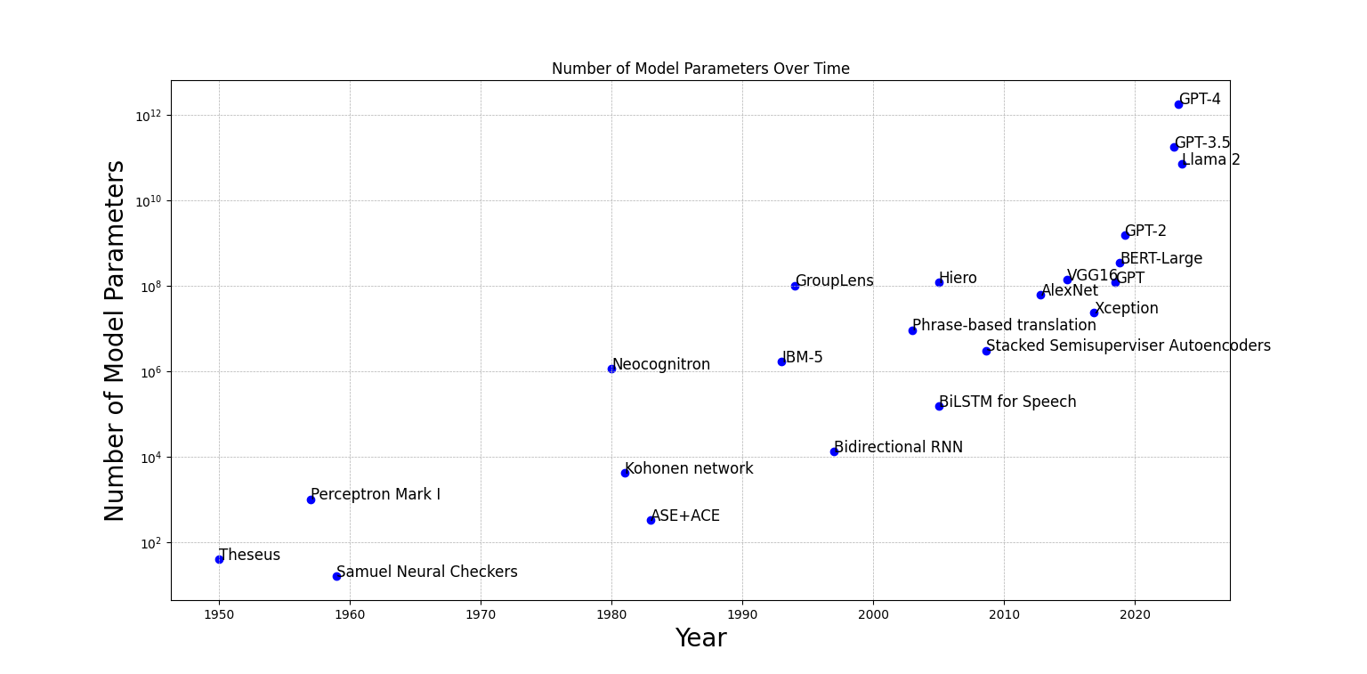
In the dynamic landscape of Artificial Intelligence (AI) [1], two notable trends have shaped its development: the exponential growth in the number of AI model parameters and the staggering amount of data generated. These factors have propelled AI to new heights and unlocked unprecedented possibilities. The first trend revolves around the expansion of AI model parameters (Figure 1). In recent years, there has been a remarkable surge in the size and complexity of deep neural networks (Figure 2b). This is primarily due to the advent of deep learning, a subfield of AI that utilizes multi-layered neural networks to process and analyze data. Deep learning models have shown remarkable capabilities in tasks such as image classification, natural language processing, and speech recognition. The increase in the number of parameters within these deep learning models has played a significant role in their success. By augmenting the model’s capacity to learn intricate patterns and representations, larger networks can often achieve superior performance. Large language models (LLM) [2], such as chatGPT for example, have achieved unprecedented scale and complexity. It’s reported that GPT-3 and GPT-4 consists of approximately 175 billion and 1.8 trillion parameters, respectively. These parameters serve as the variables that the model learns and adapts from training data, enabling it to generate coherent and contextually relevant text responses from prompts. This remarkable expansion has been made possible by advancements in computational hardware, such as Graphics Processing Units (GPUs) and specialized hardware accelerators like Google’s Tensor Processing Unit (TPU), which enable the efficient training and inference of such complex models. Simultaneously, the second trend highlights the explosion of data generation. In the digital era, it is estimated that around 2.5 quintillion bytes (2.5 exabytes, exa=) of data are created daily, and over the next three years up to 2025, global data creation is projected to accumulate to more than 180 zettabytes (zetta=). From social media interactions and online transactions to sensor measurements and scientific research, this data serves as a rich resource for training and fine-tuning AI models. The availability of vast and diverse datasets has in turn revolutionized the field of AI. Data-driven approaches, often referred to as "big data", have enabled AI models to learn from enormous amounts of information, leading to improved accuracy and robustness. Additionally, advancements in data storage, processing, and cloud technologies have made it easier to handle and analyze massive datasets efficiently. The increased capacity of large models to capture and represent complex relationships, coupled with the abundance of training data, has facilitated breakthroughs in diverse domains, including healthcare, finance, transportation, robotics, metaverse, and natural language understanding.
However, this growth is not without challenges. The large number of model parameters and the amount of data required for training pose significant computational and resource-intensive requirements. Developing new hardware and techniques to scale AI models efficiently, along with addressing concerns related to latency, parallelism, and energy consumption, are areas that researchers and engineers are actively exploring.
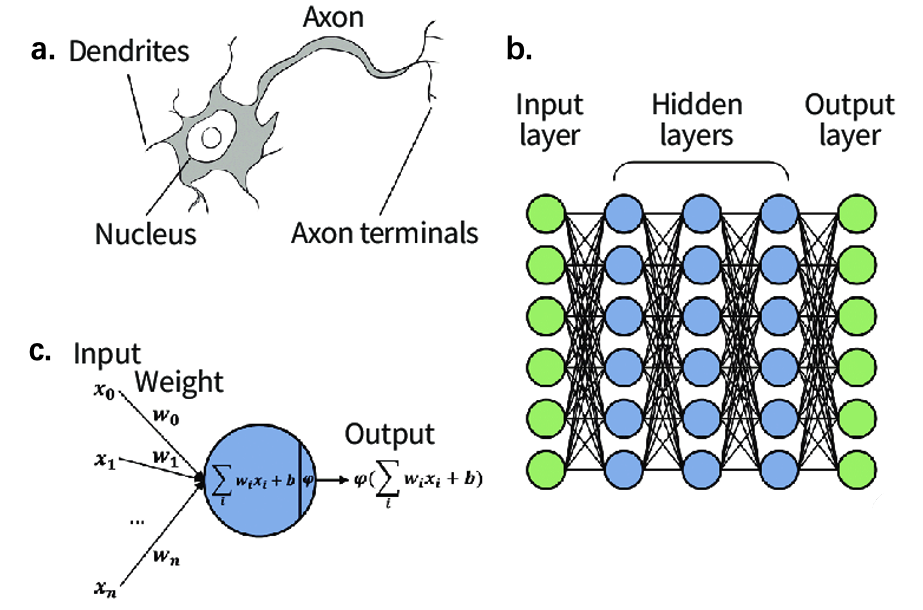
Neuromorphic computing [3, 4, 5, 6, 7], an emerging field of research, focuses on developing computational systems inspired by the structural and functional characteristics of the human brain. This discipline strives to overcome the limitations of conventional computing by mimicking the parallelism, fault tolerance, and energy efficiency observed in biological neural networks (Figure 2a). At its core, neuromorphic computing aims to create hardware and software architectures that replicate the behavior of neurons and synapses. These architectures enable the processing of information using spiking neural networks and specialized neuromorphic chips, which offer real-time handling of complex data and the potential for accelerated machine learning algorithms. The primary advantage of neuromorphic computing lies in its ability to process information in a massively parallel manner, leading to enhanced computational and energy efficiency. By leveraging the inherent capabilities of neurons and synapses, neuromorphic systems demonstrate potential applications in areas such as pattern recognition, image classification, autonomous driving, and LLM. In hardware design, researchers are exploring novel components like micro-ring resonators and VCSEL lasers to emulate synaptic connections or to perform matrix operations. These photonic components enable the creation of highly efficient AI hardware that can adapt and learn from input data, similar to the plasticity observed in biological neurons. Neuromorphic techniques enable the development of self-learning systems capable of processing sensory input and making intelligent decisions in dynamic environments to facilitate the growth of AI.
In the field of optical computing, nanophotonic devices which utilize optical near-fields and effective interactions are very important. Key components within neural networks (Figure 2b-c), such as activation functions [8, 9, 10, 11] and backpropagation [12], currently represent the focal point of research in the realization of optical neural networks. Y. Zuo et. al. demonstrated an all-optical neural network (AONN) which can work with nonlinear activation [11]. They used spatial light modulators and Fourier lenses to realize programmed linear operations and laser-cooled atoms with electromagnetically induced transparency to realize nonlinear activation function. In this device, linear operations are done via Fourier transform and all diffracted beams in the same direction are summed onto a spot, which can be expressed as (Figure 2c). In this formula, W is weights, x is input, and b is bias. When nonlinear operations are also done, we can get the final output , where is a nonlinear activation function (Figure 2c). It is obvious that this neural network which uses Fourier lenses is easy to construct, low in power consumption, and boasts rapid computational speed. However, as a neural network system, the Fourier optical lens system might be excessively bulky.
Another all-optical neural network, termed "D2NN”, is considered as a potential contender for miniaturized all-optical diffractive deep neural networks [13]. In this system, each point on a specified layer is a neuron, and has a designed transmission or reflection coefficients. When it works, the input of each layer is defined by previous layer based on free-space diffraction. In this work, the device is on the macro-scale as it spans a few centimeters in length and width, and a few millimeters in thickness. However, this is because it operates in the terahertz range, and if altered to function in the near-infrared range suitable for optical communications, its size could potentially be reduced by a few hundred times. The fabrication of such tiny devices currently presents a significant challenge, yet D2NN remains a viable contender for integrated AONN systems.
With its rapid development, relative maturity, and high degree of integration, silicon photonics emerges as a compelling candidate for the integration of AONN. In silicon photonic integrated circuit, the Mach-Zehnder Interferometer (MZI) can regulate the intensity of optical signals through light interference. By amalgamating multiple MZIs, we can form an integrated optical neural network (ONN) on-chip. In 2017, Y. Shen et. al. proposed an AONN based on cascaded array of 56 programmable MZI in a silicon photonic integrated circuit [14]. By programming the internal and external phase shifters of each MZI, this system enables arbitrary SU(4) rotations and finally expresses unitary matrices. The splitting ratio and the differential output phase are controlled when the operations between unitary matrices are done. In 2019, I. Williamson et. al. added nonlinear activation function operating on MZI phase shift and realized nonlinear activation function on on-chip AONN [8]. They improved test accuracy on the MNIST task from 85% to 94%.
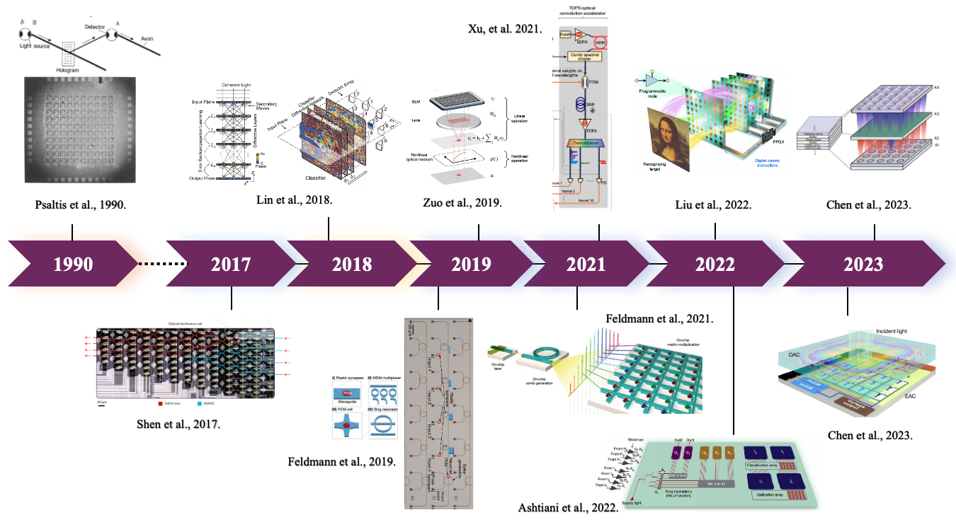
With earlier development of nonlinear activation functions, AONNs, and D2NNs that serve as the building blocks of photonic neuromorphic computing, researchers later began to explore nanophotonic devices such as frequency microcombs [15], micro-ring resonators [16], lasers [17], metasurfaces [18], optical attenuators [19], and photodiodes [19] etc. to realize more advanced neuromorphic functionalities. We can roughly categorize existing efforts into three branches: 1. simulate the principles of forward propagation in an artificial neuron; 2. achieve image classification or pattern recognition; 3. realize convolutional operations by performing matrix-vector multiplications (MVM). A full timeline of the evolution of photonic neuromorphic systems is shown in Figure 3.
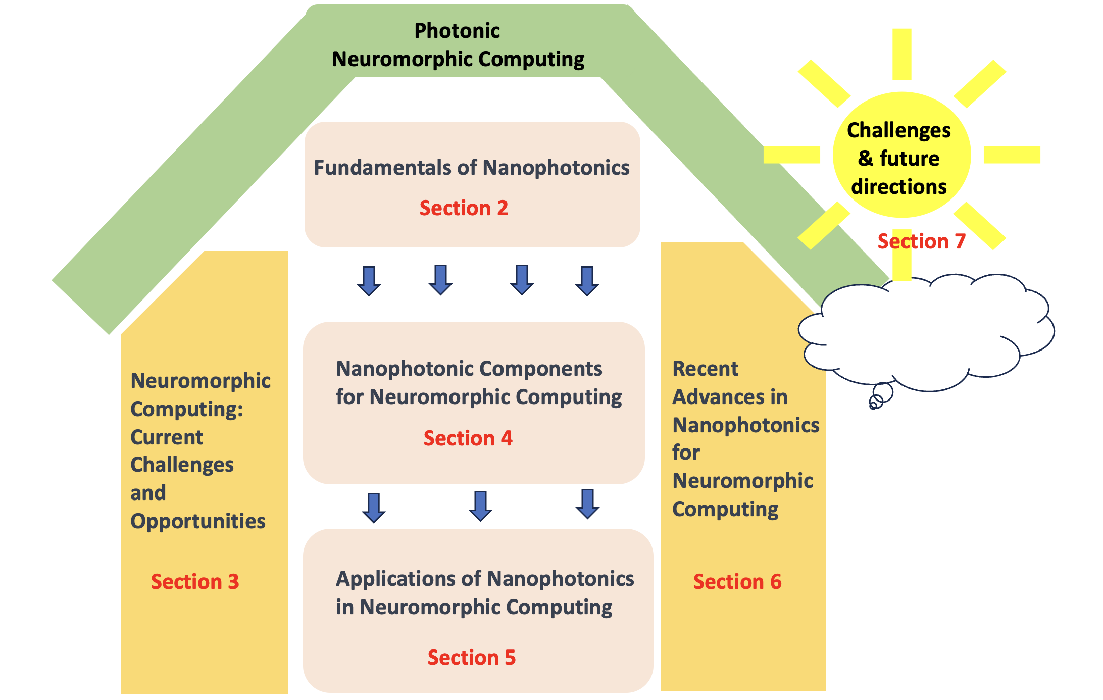
About a dozen reviews have been written on the topic of photonic neuromorphic computing systems. Some place heavier emphasis on a specific aspect of the system such as spike generation, synapses or nonlinearity, and some focus on specific structures such as MZI, frequency combs, or diffractive layers, and some others tend to discuss the relationship between photonic neural networks and machine learning via the bridge of multiply-accumulate operations (MAC) and wavelength division multiplexing (WDM). This review, however, aims to concisely and comprehensively unify each of the aforementioned aspects of photonic neuromorphic design and dissect them from the perspective of photonic engineering and materials science; as a result, details/fundamentals of the theories of neural networks or computing systems will not be fully addressed here. According to Figure 4, the review is organized as follows: Sec. 1 Introduction. Sec. 2 Fundamental of nanophotonics, introduces theories and principles of nanophotonics. Sec. 3 talks about the advantage of neuromorphic computing over conventional digital electronics-based or von Neumann computing. Sec. 4 covers existing nanophotonic components and fab platforms for neuromorphic computing. Sec. 5 details the applications of nanophotonics in neuromorphic computing, providing a summary of the evolution of photonic neuromorphic paradigms over time (also graphed in Figure 3). Sec. 6 addresses recent advances in nanophotonics for neuromorphic computing, including topological insulators and PCSEL lasers. Sec. 7 discusses the challenges and future directions in photonic neuromorphic computing. Finally, Sec. 8 summarizes the review by providing a conclusion and closing marks.
2 Fundamentals of Nanophotonics
2.1 Basics of photonics and light-matter interactions at the nanoscale
Nanophotonics is a multidisciplinary field that studies light propagation and light–matter interaction at nanoscale, which has applications in various fields such as optical sensing [23], optical interconnection, and optical communication [24]. Nanophotonics also plays an important role in developing optical computing systems, providing an alternative to electronic computers for high-speed and low-power data processing and transmission [25, 26]. This section introduces the basics of photonics in light-matter interactions.
Maxwell’s equations constitute the cornerstone of classical electrodynamics, delineating the fundamental principles underlying the dynamical behavior of electric and magnetic fields. These equations encapsulate the generation of electromagnetic fields by charges and currents (Gauss’s law for electricity and Ampère’s law with Maxwell’s addition), the non-existence of magnetic monopoles (Gauss’s law for magnetism), and the induction of electric fields by time-varying magnetic fields (Faraday’s law of induction). In the context of light-matter interactions, Maxwell’s equations are indispensable. They predict the self-propagating nature of electromagnetic waves in a vacuum, a phenomenon in which light is a principal exemplar. Upon interaction with matter, these equations govern the complex processes of reflection, refraction, absorption, and transmission. The boundary conditions dictated by Maxwell’s equations at interfaces between different media determine the electromagnetic field distributions and, consequently, the optical responses of materials. Furthermore, Maxwell’s equations are integral to the quantification of the dielectric and magnetic properties of materials, characterized by permittivity and permeability, respectively. These properties influence the phase velocity of electromagnetic waves in media, leading to phenomena such as dispersion and polarization. The equations also describe the conservation of energy and momentum in electromagnetic fields, providing a framework for understanding the interaction forces and torques exerted by light on material particles, which is the basis for optical trapping and manipulation technologies.
| (i) | ||||
| (ii) |
| (iii) | ||||
| (iv) |
Maxwell’s equations form the foundation of nanophotonics and light-matter interactions.
To build efficient optical neural networks (ONN), nanoscale components are required to manipulate and process light signals. Diffraction and interference of light at the nanoscale indeed play a crucial role in these components. These phenomena enable precise control over light signals, allowing for information encoding, processing, and transmission within the network. In principle, diffraction and interference both arise due to the superposition principle, which states that when two or more waves overlap, the resulting wave is the sum of their individual amplitudes. For example, the photonic oscillations and produced at a certain point by coherent light waves can be expressed as,
So, it can be readily deduced that the resultant superimposed oscillation is
Where
It is obvious that by varying and , both the amplitude and phase of the combined light wave are changed. By architecting specialized dielectric material structures on a nanoscale, intricate photonic interactions can be actualized.
For example, B. Wu et. al. actualized a variety of nonlinear activation functions through the employment of the thermo-optic effect and micro-ring resonators [27]. They use germanium whose absorption coefficient and refractive index are characterized by temperature as follows:
Where and are constant and is change of temperature. These two values have influence on quality factor of micro-ring resonators, and thus change the output power of it. Another example is MZI, which is a device that utilizes the principle of light interference to measure small changes in phase or refractive index [28]. It consists of a beam splitter that splits an incoming light beam into two paths, which then recombine at a second beam splitter. However, we can also utilize the electro-optic effect and nonlinear effects to alter the refractive index and phase, modify the interference conditions in MZI, and finally realize the change of light wave amplitude.
2.2 Principles of nanophotonics in neuromorphic computing
Similar to electronic computing, in optical computing, logic gate serves as the very bedrock upon which systems are constructed. In recent years, notable advancements have been achieved in the field of optical logic gates, which have paved the way for neuromorphic computing [29]. The realization of optical logic gates have many different strategies, such as diffractive neural networks [13], semiconductor optical amplifiers [30, 29, 31] and photonic crystal waveguide [32].
Diffraction neural networks largely rely on the physical phenomenon of diffraction for computation. Typically, these networks undergo a pre-training process wherein they learn the intricate relationship between the input light field and the resulting patterns. This learning procedure is accomplished by adjusting the phase delay or transmission rate at each specific point in the network. Diffraction neural networks are generally composed of multiple metasurfaces [13, 33, 34], each layer equating to a layer of neurons. With suitable training, manufacturing the corresponding diffractive network layers, and assembling them rightly, it can execute the required operations on any given input light field in real-time while performing neural network calculations at the speed of light. Diffraction neural networks operating in the mid-infrared are anticipated to function within a scale of a few millimeters. This endows it with immense prospects for large-scale integrated applications.
Semiconductor optical amplifiers (SOAs) are used to form optical logic gates due to their ability to modulate the intensity of light, change the phase of light, or both [30]. They can perform several different logical operations based on the principle of gain saturation, where the output light intensity is dependent on the input light intensity. This characteristic makes SOA highly valuable for building optical logic gates, enabling it to implement various applications such as all optical lattices, pseudo-random bit sequence generation, and all optical encryption.
Photonic crystal waveguides are structures that can limit and guide light in periodic dielectric media. They can control the propagation of light in a highly precise manner, making them an excellent platform for implementing optical logic gates. Especially in recent years, the emerging topological photonic crystal waveguides [35, 36, 37, 38] have significant advantages in the construction of all-optical logic gates due to their unidirectional propagation, controllable splitting, and other attractive characteristics.
These advancements in optical logic gates above have made optical neuromorphic computing a promising field for the development of high-speed, low-energy, and compact computing systems. In more recent years, researchers have begun to explore more sophisticated nanophotonic devices such as frequency microcombs [15], micro-ring resonators [16], phase change materials [15], nanolasers [17], metasurfaces [18], optical attenuators [19], EDFA [16], and photodiodes [19] ] to achieve state-of-the-art neuromorphic computing systems. These will be discussed in detail in the remaining text.
3 Neuromorphic Computing: Current Challenges and Opportunities
3.1 Brief overview of traditional computing and its limitations
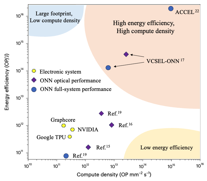
With the development of electronic device and improvement of the computing performance, many changes taken place in human society, and many scientific fields have made numerous breakthroughs. In order to meet the needs of scientific development, the size of electronic device is required to continue to scale to support the continuous growth of computing performance and maintain this increasing trend [39]. In particular, nowadays, because of the fast-paced advancements of AI, LLMs, Internet of Things (IoT), metaverse, and cloud computing, the amount of data has virtually exploded and the demand for high-performance memory and computing efficiency has become higher and higher [3, 40]. However, there are currently some difficulties that need to be addressed urgently. On one hand, as the Moore’s law comes to its end, the required performance gains can no longer be achieved through conventional scaling device [41, 39]. On the other hand, at present, most computers that are general-purpose devices are designed based on the traditional Von Neumann architecture. Limited by the bottlenecks of hardware fabrication technology and the inherent structural problems such as “memory wall”, conventional von Neumann architecture can not sustain processing large amounts of data in the AI era [41, 4]. So it is critical to propose alternative architectures that scale beyond von Neumann to break through the computing bottlenecks. Figure 5 plots figure of merit (FoM) of existing digital electronic hardware and emerging photonic neuromorphic systems as AI accelerators. By comparison, photonic neuromorphic systems outperform electronic hardware in both energy efficiency and compute density.
3.1.1 Brief Overview of traditional computing
Progress in computing field has significantly relied on the semiconductor devices miniaturization. In 1965, Intel cofounder Gordon Moore paid attention to stable growth rate of miniaturization and published a prediction known as “Moore’s Law”, which states that the number of transistors in each new-generation of computer chips would double every two year [42]. With the miniaturization of transistors, the density of transistors in chips increases continuously, and computing capability is also becoming stronger and stronger. Moore’s Law has driven progress in many aspects of computing, such as better CPU performance, improved energy efficiency, larger storage capacity and better cost savings [43]. Moreover, a computer architecture named the “Von Neumann Architecture” revolutionized computing as Moore’s Law took effect, and enabled hardware engineers to build a variety of computational systems [4].
Von Neumann Architecture, also known as the Princeton Architecture, is the fundamental organizational structure of a digital computer based on the principles proposed by mathematician John von Neumann. It treats instructions (the computer program) as a special type of data and stores instructions and data in different addresses in the same memory. The main characteristics of Von Neumann architecture are: adopting a binary system and computing executes in procedural order. The invention of the von Neumann architecture laid the foundation for modern computer architectural concepts [44].
Conventional digital computers are built on the Von Neumann architecture and based on the silicon microelectronics platform. Generally, a Von Neumann computer is mainly composed of a memory bank for storing data and instructions and a central processing unit for performing nonlinear operations and connecting transmissions between the two [45, 46, 6]. Among them, as the core of the architecture, the CPU is composed of a control unit and an arithmetic logic unit (ALU). Usually, the CPU executes a series of instructions to process data stored in memory units through interacting with the memory system [47]. Main memory is the key to memory system and set up by adopting the Dynamic Random Access Memory (DRAM) technology. When performing computing, data in main memory needs to be processed. Because the CPU can only process the data in the cache, memory controller will send a series of instructions to the DRAM module through the off-chip bus, receive the response from the DRAM module after receiving the instructions, and then use the cache or registers to save the data [48].
3.1.2 Limitations of traditional computing
Continuous expansion in the amount of calculations and data leads to stricter requirements for high-performance, and computer architecture needs to shift from the intensive type of computing to the intensive type of memory [3]. Nowadays, because of many limitations, it is hard for traditional computing to adapt to the current development pace.
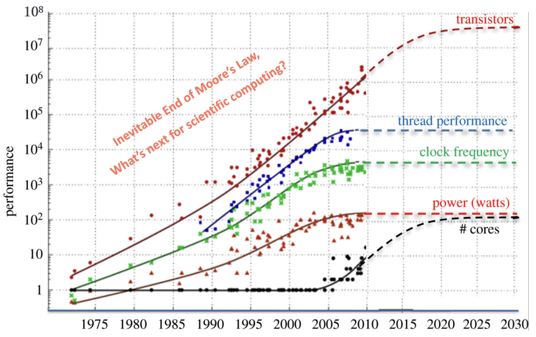
On one hand, as the scaling degree of device feature size approaching its immutable physical limit, the trend of rapid growth in aspects of speed and integration of microelectronic devices represented by complementary metal oxide semiconductors (CMOS) has slown down [3, 50]. The 10-nm technology of Intel, originally scheduled to be launched in 2016, was delayed until 2019. Apple and Samsung, despite claiming to have reached 5-nm or even 3-nm in their nanofab, can not keep up with Moore’s Law in updating their miniaturization technology [42]. Obviously, the effects of improving traditional computational performance by reducing device size have gradually weakened, and Moore’s Law that has influenced the growth of computational capability in electronic devices is inevitably coming to an end. In other words, the Post-Moore era is coming [40] (Figure 6).
On the other hand, the Von Neumann architecture on which traditional computing is built faces problems such as “ memory wall” that limits system performance, making it difficult to meet modern requirements for efficiency, energy consumption, density and cost in high-performance computing. Under the Von Neumann architecture, instructions and data are placed in the same memory, and instructions follow serial execution rules, so both of them can not be accessed simultaneously to avoid confusion in memory access [45, 51, 50]. Meanwhile, the Von Neumann architecture features a separate memory and computing architecture, where memory unit and computing unit remain separate [45]. During computing, data is frequently transferred between the memory unit and the processor unit, resulting in non-negligible delays and consuming a significant amount of energy. Up to now, under serial execution rules, data movement induces longer signal delay and increased energy losses, because of the huge gap between the operation speed of the CPU and the speed of accessing memory (the computing speed of the CPU has far exceeded the speed of accessing memory), the restriction caused by the bandwidth of the memory hierarchies, and the heat dissipation issue caused by unresolved leakage. These conditions ultimately result in insufficient utilization of hardware resources, increased energy consumption and decreased computational efficiency. For example, the AI facial recognition network developed by Google utilized a total of 16000 CPU cores on a three-day training session while consuming 100 kilowatts of power [52, 53, 3, 51, 50, 48, 40]. To alleviate these burdens, computing capability can be enhanced by separately increasing the bandwidth of the memory and using graphics processing unit (GPU) or AI accelerator. However, this approach has a limited benefit in terms of improving computing speed and energy consumption, and is not a long-term plan [40]. In addition, application-specific integrated circuits (ASIC) also play a role in addressing relevant issues. Compared with GPU, ASIC can significantly reduce energy consumption, but most of consumption during operation is still wasted in the data movement rather than logic operation [54].
Overall, considering the ending of Moore’s Law and the limitations of the von Neumann architecture on the further development of modern computing facilities, there is a vital need to break through the core architectural bottleneck and seek alternative architectures and paradigms to build non-von Neumann systems to prominently strengthen computing performance [52, 55].
3.2 Introduction to neuromorphic computing and its advantages
Current computer technology is facing two important bottlenecks: the memory wall effect of the "von Neumann" architecture causes low energy efficiency [57, 58, 59], and Moore’s Law, which leads the development of semiconductors, is expected to expire in the next few years [60, 61, 62, 63]. On one hand, the traditional processor architecture converts the processing of high-dimensional information into a one-dimensional processing of pure time dimension, which has low efficiency and high energy consumption [64]. This architecture cannot construct appropriate algorithms when processing unstructured information, especially when processing intelligent problems in real time. In addition, the information processing takes place in the physically separated CPU and memory. Programs and data are sequentially read from the memory into the CPU for processing, and then sent back to the memory. This process causes a large amount of energy consumption [64]. A mismatch between the rate at which programs or data are transferred back and forth and the rate at which the CPU processes information results in a severe memory wall effect [65, 66, 57]. On the other hand, as the semiconductor industry enters the sub-10 nm threshold, devices are approaching the limits of their physical shrinkage, and quantum effects are increasingly interfering with the normal operation of electronic devices [67, 68]. Although people have different estimates of the specific end time of Moore’s Law, there is no controversy in the industry about the end of Moore’s Law that has lasted for the past 50 years.
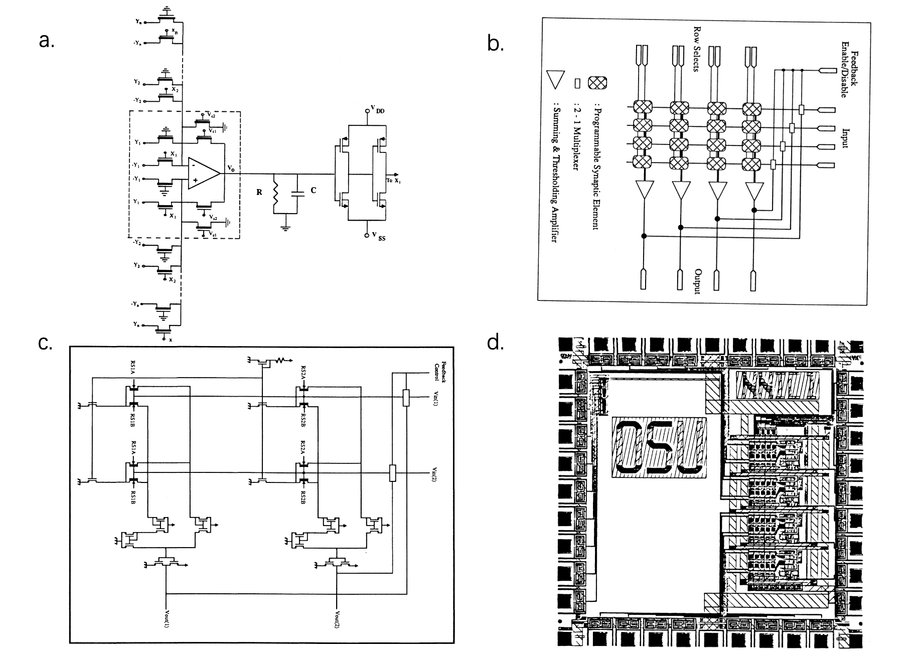
In 1989, Caltech’s Carver Mead proposed the concept of "neuromorphic engineering (or brain-like computing)" in his book titled "Analog VLSI implementation of neural systems", which uses sub-threshold analog circuits to simulate Spiking Neural Network (SNN) [56]. As shown in Figure 7, Mead showed how the powerful organizing principles of animals’ nervous systems can be realized in silicon integrated circuits, where examples include silicon neural systems that replicate animal senses. Meanwhile, Moore’s Law continued to develop, and the frequency and performance of processors based on the von Neumann architecture continued to improve, while brain-inspired computing remained stagnant for more than 10 years. Around 2004, the main frequency of single-core processors stopped growing, and while the industry turned to multi-core processors, the academic community began to seek alternative technologies such as non-von Neumann architectures. Since that point and in the following 10 years or so, neuromorphic computing has begun to attract widespread attention.
It is well known that the nervous system of mammals, especially humans, is one of the most efficient and robust structures in nature. The human brain has a large number of connections and exhibits strong parallelism. It has about neurons and synapses, but consumes only about 20W of energy [75]. Neurons achieve biological interconnection at a speed of a few milliseconds and have excellent fault tolerance mechanisms for component-level failures [76]. For computer scientists, there are tremendous similarities between neural systems and digital systems. Components such as cell body, dendrites, axons, nerve terminals, and synapses together constitute a neuron unit. Specifically, the core part of the neuron is a cell body containing a nucleus, with a radius of 2 to 60 microns; there are two types of cell processes of different lengths on the surface of the cell body, which are long axons (only one) and short dendrites (usually multiple); the excitatory transmission between neurons passes through axons and nerve terminals and finally reaches the synapse (the connection point between neurons) [77]. Neurons with various functions constitute a complete nervous system, which can effectively receive, integrate and transmit information/signal. This is considered to be the core link in the process of nervous system learning and adaptation. Although brain neural networks have different information processing and logical analysis capabilities at different levels, they are a coordinated and unified whole and are closely connected with each other [77]. The neuromorphic computer is a novel computer model that simulates the operation of the brain’s neural network with ultra large-scale pulses and real-time communication [78]. Neuromorphic computers simulate the high performance, low power consumption, real-time and other characteristics of biological brain neural networks, and use large-scale CPU/GPU clusters to implement neural networks. In the CPU cluster, each thread will map and simulate the corresponding neuron, and thousands of threads (neurons) run in an orderly coordinated manner to form a complete large-scale neural network.
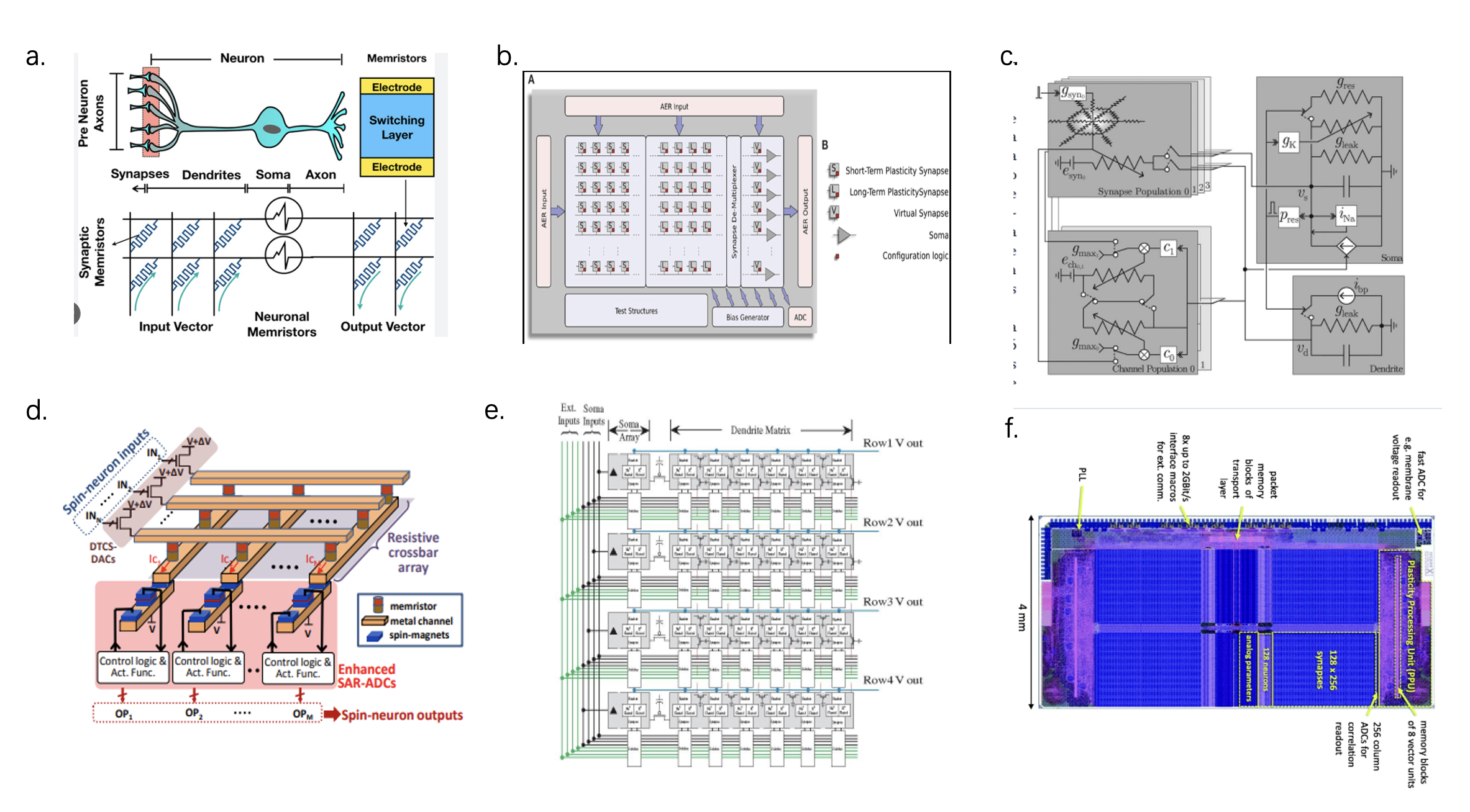
The implementation of neuromorphic computing at the hardware level can be achieved through oxide-based (CMOS) devices such as memristors, spin electronic memories, threshold switches, transistors, etc. Some examples are shown in Figure 8. Back in 2006, researchers at Georgia Tech proposed a field-programmable neural array [73]. The chip is the first in a series of increasingly complex floating-gate transistor arrays that allow the charge on the MOSFET gate to be programmed to simulate the channel ion properties of neurons in the brain, and is the first silicon programmable Neuron array. At the same time, many transistor-based brain-inspired chips and brain-inspired computer systems have also developed to a certain extent. For example, Stanford University developed the brain-inspired chip "Neurogrid" based on analog circuits, the University of Manchester began to develop SpiNNaker, a multi-core supercomputer that supports spiking neural networks based on ARM, the European Union’s FACETS (fast analog computing with emergent transient states) project, and the U.S. Defense Research Agency DARPA’s SyNAPSE (systems of neuromorphic adaptive plastic scalable electronics) project [73, 71, 79, 80, 81]. In 2008, HP realized a memristor prototype that could simulate the function of synapses, and demonstrated the first hybrid circuit of memristor and silicon materials [82]. The global craze for artificial synapses began to take off in June 2012, when spintronics researchers at Purdue University published a paper on designing neuromorphic chips using lateral spin valves and memristors [72]. They believe the architecture works similarly to neurons and could therefore be used to test methods of reproducing brain processing. In addition, these chips are significantly more energy-efficient than conventional chips. In the same year Dr. Thomas and his colleagues at the University of Bielefeld created a memristor with learning capabilities. And in the following years [83], Thomas used this memristor as a key component of an artificial brain. Because of this similarity between memristors and synapses, it is an excellent material for building artificial brains—and thus a new generation of computers. Memristor allows us to build extremely energy-efficient, durable, and self-learning processors. It is precisely because of this ability that memristors have also received increasing attention in the fields of neural networks and artificial intelligence. Several research groups are now exploring the use of memristors to build more efficient neural network architectures.
3.3 Challenges and limitations faced by conventional neuromorphic computing
The limitations of traditional brain-inspired computing mainly encompass three aspects: hardware limitations, software and algorithm limitations, and practicality and application limitations. They will be discussed in detail below in the text as well as in Figure 9, which compares biological brains, electronic, and photonic neuromorphic computing systems.
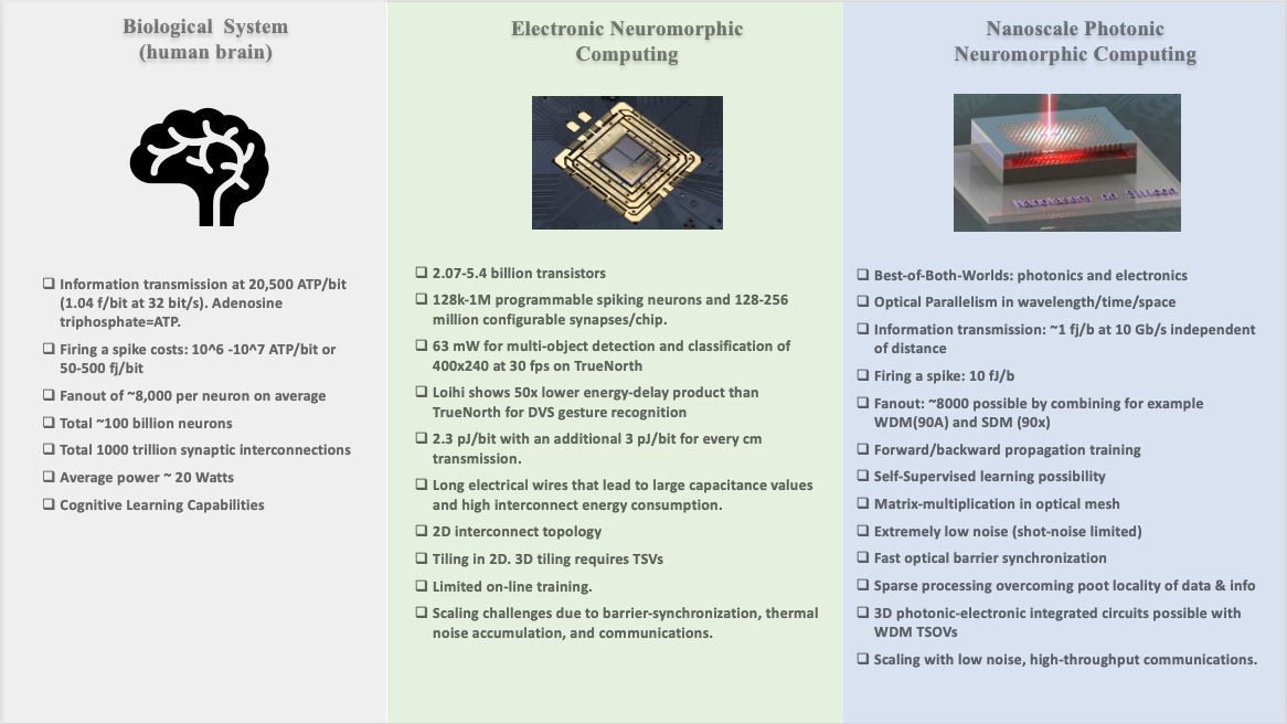
Although neuromorphic computing advertises low power consumption, existing hardware typically consumes more energy than biological nervous systems. Decades of research and billions of dollars have been invested in various forms of pattern recognition, and while substantial improvements have been made, synthetic electronic systems still fall short of the capabilities of human perception on specific problems [90, 91]. Materials play a key role in the energy consumption of neuromorphic computing. Due to the conductivity and resistivity characteristics of conventional conductors, a large amount of energy loss will inevitably occur during the transmission of electrical currents. Moreover, the size factor is also limiting the energy consumption limit of traditional conductive materials. As neuromorphic computing devices continue to shrink in size, quantum and thermal effects may become more pronounced, affecting energy efficiency [92, 5]. As seen in Figure 9, conventional electronic systems typically consume three orders of magnitude more energy than biological systems and photonic systems.
In computing systems and networks, "Communication Overhead" is a term used to describe the additional resources and time required for information transmission [93]. It is an important factor affecting the computing performance and energy efficiency. In the field of neuromorphic computing, this concept has several important aspects. First, data transmission is a core issue because simulating neurons in neural networks requires information transfer through synapses, which usually consumes additional energy and time in hardware implementation [94]. Second, the activity of neurons usually needs to be represented through specific encoding and decoding methods, which also increases computational and energy overhead. In addition, some neuromorphic computing models require precise timing synchronization between neurons, which further increases communication and computing overhead [95, 96]. In large-scale neural networks, information also requires complex routing between multiple neurons and network layers, which often requires additional hardware and algorithm support. In order to ensure the accuracy of information transmission, error detection and correction mechanisms need to be introduced, which will also bring more communication overhead [97]. Finally, under high load or high concurrency, information may need to be queued in a buffer waiting to be processed, resulting in latency and additional energy consumption [98, 99]. Therefore, communication overhead is an important factor affecting the performance and energy efficiency of brain-inspired computing, and its optimization usually requires comprehensive consideration from multiple aspects such as hardware design, network topology, and signal encoding methods. In Figure 9, it’s shown that photonic systems can transmit data at a high rate and a low energy level independent of distance, which essentially solves the communication overhead of electronic systems.
Parallelism and synchronization also influence power consumption of neuromorphic computing. In traditional electronics, parallelism and synchronization face several major limitations. First, in terms of parallelism, electronic devices are often limited by circuit bandwidth, which affects their ability to perform highly parallel processing [100, 101]. Additionally, in highly parallel electronic systems, electromagnetic interference can become a serious problem, limiting overall performance [88]. Second, in terms of synchronization, maintaining global clock synchronization can be very complex and energy-intensive in large-scale electronic systems [102]. In addition, the propagation speed of electronic signals in wires is limited, which further affects the accuracy of system synchronization. Therefore, these factors together constitute the main limitations of traditional electronic devices in terms of parallelism and synchronization. Photonic systems, on the other hand, can achieve high-degree of parallelism using the inherent fanout and WDM techniques , depicted in Figure 9.
In addition to the limitations of energy consumption of conventional neuromorphic computing, imitating large-scale neural networks requires a large amount of hardware resources, which is impractical in terms of space and cost.
To mimic large-scale biological neural networks, large numbers of neurons and synapses are needed. This results in larger hardware size or footprint, which increases cost and space requirements. For example, BrainScaleS is a nuromorphic computing system for large-scale simulations, which requires a full-sized dedicated computer room to accommodate it [74]. Neurogrid, A hardware platform that simulates cortical neural networks, comes in a size equivalent to a standard 19-inch rack [71]. On the other hand, quantum effects make it impossible to further reduce the size of transistors and therefore the size of brain-like computers [68, 103]. Moreover, the complex interconnection structure between neurons faces huge challenges in hardware implementation, especially when pursuing low power consumption and high performance. Specifically, neuromorphic computing involves a series of complex dynamics and nonlinear operations, which undoubtedly increases the complexity of hardware and algorithm design. At the same time, simulating biological neural networks usually requires storing a large amount of parameters and status information, which not only places higher requirements on storage resources, but also has a considerable impact on system size and energy consumption [74]. As the network scale expands, how to effectively expand hardware scaling and maintain low energy consumption becomes particularly critical. In this context, integrating multiple components such as neurons, synapses, and learning rules into an efficient operating system becomes a difficult task. Finally, it is worth noting that existing semiconductor processing technology also has certain limitations in terms of integration density, power consumption and reliability [104]. Therefore, solving these problems of size and complexity requires interdisciplinary research collaboration and continued technological innovation in the industry.
Last but not least, in the field of neuromorphic computing, software and algorithms face a series of challenges and limitations as well. First, the software implementing these models is often extremely complex and computationally intensive due to the complex neurodynamics and nonlinear calculations involved [6]. This complexity not only limits the feasibility of the algorithm in practical applications, but also increases the computational burden. Secondly, especially in applications based on spiking neural networks (SNNs), the algorithm training process often requires a large amount of time and computing resources, which poses an obvious obstacle to scenarios that require real-time or near-real-time response [95]. Furthermore, compared with traditional machine learning algorithms, neuromorphic algorithms are often more difficult to interpret and verify, which is particularly problematic in applications that are highly sensitive and require interpretability, such as medical or autonomous driving [105]. In addition, most of the existing brain-inspired algorithms are developed on traditional computing platforms that do not fully match the brain-inspired hardware architecture. This mismatch often leads to algorithm performance degradation in real hardware environments. At the same time, although the learning rules and plasticity mechanisms in biological neural networks are extremely complex, current algorithms fail to fully simulate these advanced characteristics, thus limiting their effectiveness in handling more complex real-world tasks [78]. Finally, although brain-like algorithms perform well on certain specific tasks, they usually lack the versatility and adaptability to demonstrate across multiple tasks and different environments.
4 Nanophotonic Components for Neuromorphic Computing
4.1 Key devices of nanophotonics for neuromorphic computing
Nano-photonics, as an emerging interdisciplinary subject, integrates the principles of nanotechnology and photonics, aiming to explore and harness the manipulation of light wave by nanoscale structures. In the field of nanophotonics, active devices and passive devices are crucial, which as the basic components of photonics have broad application prospects. Neuromorphic systems aim to mimic the computational and cognitive capabilities of the brain by leveraging the principles of neural networks. In this part, we will focus on the key devices in nanophotonics, divided into two parts: active devices and passive devices, and provide an in-depth analysis of their working principles, applications in neuromorphic computing, and future development trends. Some representative devices are shown in Figure 10.
1. Active devices
Active devices are photonic devices that can generate, manipulate or amplify optical signals, including lasers, optical modulators, photodetectors, etc. [111] These devices play a vital role in fields such as communications, sensing, laser processing, and medical diagnosis.
1.1 Laser
Lasers are the most important and widely used active devices in nanophotonics and are known for their highly coherent light output, high emission power, and high spectral brightness [106]. In the field of nanophotonics, different types of lasers such as Vertical Cavity Surface Emitting Lasers (VCSELs), DFB lasers, micro-ring lasers, quantum dot lasers, and the latest PCSEL [112, 113] etc. are developing rapidly [114]. These lasers not only play a key role in optical communications, but are also used in fields such as Lidar, optical sensing and medical imaging. Lasers can be pulsed, continuous-wave, optically or electrically pumped, depending on their specific needs.
1.2 Optical modulator
Light modulators are used to control the intensity, phase and frequency of light in real time [107]. In nanophotonics, technologies such as electro-optic modulators and acousto-optic modulators are widely used in high-speed optical communication systems to achieve high-speed data transmission and information processing. Nanophotonic optical modulators offer the advantages of small size, low power consumption and high speed and are key components of next-generation communication systems and photonic computers [115].
1.3 Light detector
Photodetectors are important active devices in the field of nanophotonics, used to convert optical signals into electrical signals [108]. There is a wide variety of photodetectors available, including photodiodes, photodetection arrays, and single-photon detectors. These devices play pivotal roles in communications, sensing, optical imaging, and quantum information processing for next-gen photonic computing systems [116, 117].
1.4 Future Prospects of Active Devices
In the future, active devices will continue to develop in nanophotonics. The miniaturization, low power consumption and high efficiency of lasers will empower more applications, including quantum information processing and PICs. Optical modulators will continue to play a critical role in high-speed communications and Lidar. Photodetectors will usher in higher sensitivity, faster response times, and wider wavelength ranges, driving innovation in fields such as wireless communications, medical diagnosis, and optical sensing. All these devices will substantially contribute to the growth of neuromorphic computers in the near future.
2. Passive components
Passive devices refer to photonic devices that cannot generate or amplify optical signals, but they are equally essential for the transmission, control and processing of light. Common passive devices include waveguides, resonators, photonic crystals, etc.
2.1 Waveguide
A waveguide is a structure used to guide light in a desired direction, usually consisting of a high-refractive index material surrounded by a low-refractive index cladding [109]. There are many types of waveguides, including optical fiber waveguides, planar waveguides, photonic crystal waveguides, etc. They play a key role in optical communications, optical sensing, photonic chips and other fields [118]. The low transmission loss of fiber optic waveguides makes them ideal for long-distance communications, while planar waveguides are often used in optical chips to realize micro-nanoscale integrated optical components [119].
2.2 Resonant cavity
A resonant cavity is a device used to enhance light modes of specific frequencies [110]. There are many types of resonant cavities, including fiber cavities, micro-ring cavities, micro-beam cavities, etc. Resonators can be used in filtering, lasing and sensing applications, and their high-quality factors give them a special place in nanophotonics. Micro-ring cavities achieve resonance through multiple photon reflections and are widely used in micro-lasers, sensors and quantum information processing [120, 121, 122]. They can also be used along with soliton microcombs to perform wavelength division multiplexing. A nanobeam cavity [123] is an elongated waveguide with a micron-scale cross-section that can be used to achieve a high-quality factor resonator whose size and shape can be tuned for specific applications. Key performance metrics of resonant cavities are the Q-factor and modal volume.
2.3 Photonic crystal
Photonic crystal is a material with a periodic structure that can realize the light band gap and waveguide mode of light [124, 125]. It has a periodically varying refractive index enabled by an array of holes or rods. These band gap and waveguide modes can be used in optical filtering, lasers, sensors, and other applications [126, 127]. Photonic crystal design and preparation technology plays an important role in laser designs, such as the popular Photonic Crystal Surface Emitting Lasers (PCSEL) [113] and the more recent topological insulator lasers.
2.4 Future prospects of passive components
In the future, the development of passive devices will continue to promote the development of neuromorphic computing technologies. The design of the waveguide will be more flexible to meet the needs of different applications. The resonant cavity will further improve the quality factor and allow optical devices to operate more efficiently. The structure and function of photonic crystals will be further expanded to meet the requirements of a wider range of engineering applications. The continued development of these passive devices will bring more possibilities to the future of nanophotonics-enabled areas.
We can agree that active devices such as lasers, optical modulators, and photodetectors provide optical signal generation and processing capabilities, supporting applications such as optical communications, medical imaging, and quantum information processing. Passive devices such as waveguides, resonators and photonic crystals provide key tools for light transmission and manipulation, supporting the development of optical communications, sensing applications and optical devices. In the future, these key devices will continue to be enhanced while nanophotonics continues to drive cutting-edge research in neuromorphic computing, opening up new possibilities for future scientific and engineering applications.
4.2 Optical interconnects for scalable neuromorphic systems
Neuromorphic systems, inspired by the structure and function of the brain, have attracted significant attention in the fields of artificial intelligence and computational neuroscience. Neuromorphic systems aim to mimic the computational and cognitive capabilities of the brain by leveraging the principles of neural networks. As the complexity and scale of these systems increase, the need for efficient, high-bandwidth connectivity becomes increasingly important, because providing efficient and scalable connections to support the massive flow of data between neurons and synapses is critical [128]. Traditional electronic interconnects, despite their widespread use, still face bottlenecks in bandwidth, power consumption, crosstalk, and latency as neuromorphic systems evolve. Optical interconnects, which use photons to transmit information, have emerged as a promising solution to address the limitations of traditional electronic interconnects in neuromorphic computing. In this part, we provide an overview of recent developments in the field of optical interconnects for scalable neural systems, highlighting key advances, challenges, and prospects. We draw insights from numerous research papers, focusing on advances in photonic components, network topologies, and system integration. Some representative optical interconnects are shown in Figure 11.

4.2.1 Advancements in Photonic Components
The photonic components are fundamental components of optical interconnects. Recent innovations in this field have significantly improved the performance and efficiency of optical interconnects for neuromorphic systems.
Photonic integrated circuits (PIC)
Photonic integrated circuits are compact and complex devices that combine multiple optical functions on a single chip. Recent developments in PICs have led to improved signal processing capabilities, allowing the implementation of complex neural network architectures. PICs enable efficient signal routing, switching, and conditioning in neuromorphic systems [129, 133].
Nonlinear Optical Devices
Nonlinear optical devices, such as optical parametric amplifiers [130] and inverters, have found application in improving the efficiency of optical interconnects. They enable wavelength conversion and amplification of optical signals, reducing the need for power-consuming electronic repeaters [134].
Photonic Neural Network Accelerators
Research is underway to develop specialized photonic devices to accelerate neural network (deep learning) computations. Optical processors based on metasurface layers, soliton microcombs, VCSELs, and ring resonators can perform MVM at extremely high speeds, significantly improving the efficiency of deep learning in neuromorphic systems [7, 94, 15].
4.2.2 Evolution of network topology
Network topology in neuromorphic systems is essential for efficient learning and information transfer. Recent research has explored new optical network architectures to improve scalability and system performance.
Reconfigurable optical interconnects
Reconfigurable optical interconnects provide flexibility in neural network configuration. By dynamically changing the connections between neurons and synapses, these connections enable rapid adaptation and learning [135, 136, 131, 137]. Research has focused on developing tunable optical components and switches to facilitate reconfiguration.
Neural Network-on-Chip (NoC)
Neural NoCs are specialized optical interconnects designed to efficiently connect various processing elements, including neurons and synapses. They reduce communication congestion and provide low-latency, high-bandwidth connections [132]. Recent developments have demonstrated the benefits of NoC in large-scale nervous
systems.
4.2.3 System Integration and Challenges
The integration of optical interconnects into neuromorphic systems poses several challenges related to compatibility, scalability, and power consumption.
Hybrid Integration with Electronics
Integrating optical interconnects with existing electronic neuromorphic systems is a complex task. Researchers are working on hybrid integration techniques to ensure seamless communication between electronic and photonic components, maximizing the benefits of both technologies [138, 139]. Heterogeneous and monolithic integration of semiconductor materials in optical interconnects are also a category of hybrid integration that is under intensive research.
Scalability
Scalability is a key challenge for optical interconnects. As neuromorphic systems grow in size, ensuring that optical components can be manufactured and interconnected at scale without a significant increase in cost and complexity is essential [140, 141].
Power consumption
Although optical connections are more energy efficient than electronic connections, minimizing power consumption is still a top priority. Research is ongoing to develop low-power photonic components and advanced power management techniques [102] for neuromorphic systems.
In short, optical interconnects have the potential to revolutionize the field of neuromorphic computing by providing scalable, high-bandwidth, and energy-efficient communications paths. As research on photonic components, network topologies, and system integration continues to bloom, we can expect significant advances in the development of large-scale neuromorphic systems. Integrating optics into neuromorphic hardware promises to accelerate advances in AI, cognitive computing and a range of applications, including robotics, autonomous vehicles and biomedical research. Recent advances in these three areas discussed above are paving the way for efficient and scalable neuromorphic systems. While challenges regarding compatibility, scalability, and power consumption remain, the promise of optical interconnects to revolutionize neuromorphic computing is becoming increasingly clear.
4.3 State-of-the-art fabrication platforms for nanophotonic devices
Nanophotonics is a multidisciplinary field concerned with manipulating light at the nanoscale, often on the order of the wavelength of light. This field has grown rapidly due to its potential applications in telecommunications, sensing, imaging, and computing. Nanophotonic devices offer advantages such as higher speed, lower power consumption, and compact size, but making these devices requires advanced manufacturing techniques capable of precise design of nanostructures. In this part, we provide an overview of the state-of-the-art manufacturing platforms for nanophotonic devices. We explore recent developments in lithography, etching, self-assembly and 3D printing, demonstrating their potential to revolutionize the field of nanophotonics.
4.3.1 Lithography
Lithography plays an important role in the production of optical devices and includes a variety of methods, including traditional lithography, extreme ultraviolet (EUV) lithography, beam exposure electronics and nano-printing technology.
First of all, traditional photolithography [142] is a popular technology for manufacturing optical devices. It uses a UV light source and a mask to expose the photoresist, then transfers the pattern to the optical material by chemical etching. This technology is widely used to create microscopic arrays, waveguides, sensors and other optical components. With the continuous improvement of equipment, traditional photolithography techniques have achieved higher resolution and alignment accuracy [143]. EUV lithography is an innovative method that uses an ultraviolet light source for exposure. EUV lithography has extremely high resolution and can handle more complex structures. It is widely used in the semiconductor industry but also has great potential in the production of optical devices, such as micro-lasers and optical communication components.
Electron beam exposure technology is a high-resolution preparation method that uses a precise electron beam to expose the photoresist. This method is often used to make optical devices that require extremely high precision, such as terahertz detectors and quantum dot arrays. Electron beam exposure technology can achieve preparation precision of less than 100 nanometers, which is very beneficial for the fabrication of fine structures [144].
In addition, nanoimprinting is an emerging method that reproduces micro- and nanostructures by applying pressure to the material surface. This technique is suitable for fabricating large-area structures such as nanoarrays and surface plasmonic resonators [145, 146]. This shows the potential of high-throughput manufacturing to increase production efficiency.
In short, the diversity of photolithography offers a multitude of tools and methods for fabricating optical devices. Whether traditional lithography, EUV lithography, electron beam exposure or nanoimprinting, they play a key role in innovations in photonics and optoelectronics, driving optical equipment with high performance, high resolution and high reliability. As state-of-the-art lithography techniques and tooling continue to improve, it is natural that photonic devices will become more precise and complex, supporting further development of optical communications, neuromorphic computing and laser applications.
4.3.2 Etching
Etching technology [147] is a key micro-nano processing method that is widely used in the fields of photonics and optoelectronics to accurately shape and regulate the surface and structure of optical materials. Reactive Ion Etching (RIE), for example, uses a combination of chemical and physical reactions to remove material from a substrate and is the simplest process that is capable of directional etching. A highly anisotropic etching process can be achieved in RIE through the application of energetic ion bombardment of the substrate during the plasma chemical etch. The RIE process thus provides the benefits of highly anisotropic etching due to the directionality of the ions bombarding the substrate surface as they get accelerated towards the negatively biased substrate, combined with high etch rates due to the chemical activity of the reactive species concurrently impinging on the substrate surfaces.
The main application areas of etching include waveguides, gratings, lasers, optical modulators, etc. First, etching technology plays a crucial role in waveguide fabrication. Waveguide is a basic component of optical signal transmission. Complex waveguide structures can be produced through etching technology, including straight waveguides, curved waveguides and waveguide gratings, thereby achieving efficient guidance and coupling of optical signals [148]. The preparation of gratings and nanolasers is also inseparable from the etching technology. Gratings are used for spectroscopy and spectral analysis. By making micron-scale periodic structures (like holes or rods) on semiconductor materials, optical signals of specific wavelengths can be separated [149]. Lastly, Lasers require high-precision preparation and delicacy, and etching can be used to precisely define the size and shape of the laser resonance cavity to ensure stable and efficient laser performance [150].
At the same time, optical modulators are indispensable devices in optical communications and optical signal processing, and are often prepared using etching technology. Etching techniques can be used to create gratings or modulation regions. By modulating the properties of these structures, modulation and control of optical signals, including amplitude, phase and frequency, can be achieved. In short, the application of etching technology in optical devices provides key support for the development of photonics and optoelectronics. By precisely controlling optical structures, etching technology enables optical devices to achieve higher performance, greater scalability, and greater reliability, thereby driving advances in neuromorphic computing and photonic integrated circuits.
4.3.3 3D printing technology
3D printing technology [151], also known as additive manufacturing, has emerged in the production of optical devices, bringing many potential applications and innovations to the field of photonics and optoelectronics. This technology uses a layer-by-layer method of stacking materials, allowing the fabrication of complex optical structures while providing a high degree of customization and personalization.
3D printing technology has many applications in the production of optical components. Complex optical components such as optical lenses, gratings, waveguides and reflectors can be precisely manufactured using 3D printing technology. This approach not only provides more flexible preparation but also reduces the number of optical components in the optical path, thereby reducing system complexity [152], and 3D printing technology also plays a key role in manufacturing micro-optical devices. Micro-optical components such as micro-lenses and micro-lens arrays can be manufactured with high precision using 3D printing technology to meet the needs of micro-optical systems [153, 154]. This is essential for applications such as micro cameras, biosensors and pico-projectors. In addition, optical waveguide fabrication also benefits from 3D printing, which can be used to create complex waveguide structures for efficient optical signal transmission. This is important for optical switches in data centers and optical communications because they deliver better performance and greater scalability. Therefore, by precisely controlling the arrangement and structure of materials, personalized photonic materials with special optical properties can be obtained [155, 156] for advanced computing tasks.
In short, 3D printing technology offers a new approach to manufacturing optical devices, with a high degree of flexibility and customization in the preparation process. This technology has made significant progress in the fabrication of optical components, micro-optical devices, optical waveguides and photonic materials, providing more opportunities for the development of photonics and optoelectronics. As 3D printing technology continues to develop and innovate, we will see its broader adoption in neuromorphic engineering.
4.3.4 Challenges and Future Directions
While remarkable progress has been made in nanophotonic fabrication, several challenges remain:
Integration: efficient integration of various nanophotonic components into functional systems, such as a PIC, is a complex task that requires interdisciplinary collaboration. Some existing integration methods include: heterogeneous, monolithic, hybrid integration etc.
Scalability: many manufacturing methods need to be adapted to large-scale production to meet the growing demand for nanophotonic devices. Current photonic manufacturing has relatively poor scalability compared to electronic ICs.
Materials innovation: the development of new materials with tailored optical properties will expand the design possibilities of nanophotonic devices. Core semiconductor materials, besides the typicel Silicon, are Gallium Arsenide, Indium Phosphide, Silicon Nitride, and Transition-metal dichalcogenide (TMDCs).
Cost-Efficiency: reducing the cost of fabrication techniques, especially for lithography, 3D printing and self-assembly, is essential for widespread adoption of photonic devices. This could also call for cheaper fabrication tools and equipment.
Hybrid Platforms: combining different fabrication methods can offer unique advantages, leading to hybrid nanophotonic platforms. Common semiconductor platforms include Complementary metal–oxide–semiconductor (CMOS), carbon systems including carbon nanotubes and graphene, and the latest magnetoelectric spin–orbit (MESO) [157] etc.
In conclusion, the field of nanophotonics has witnessed substantial advancements in fabrication platforms, enabling the creation of intricate and efficient photonic devices. Lithography, etching, self-assembly, and 3D printing have all played pivotal roles in shaping the future of nanophotonics. With continued research and innovation, nanophotonic devices are poised to revolutionize a wide range of applications, from telecommunications and neuromorphics to medical imaging and AI, ushering in a new era of photonics on the nanoscale.
5 Applications of Nanophotonics in Neuromorphic Computing
Figure 9 systematically compares biological, electronic, and photonic neuromorphic computing systems across the board. Key metrics / FoM being compared include: energy consumption, parallelism, latency, noise-level, scalability, computing speed, 3D or 2D topology, and learning capacity. From Figure 9 we see that photonic systems outperform electronic counterparts in all aspects and even match the energy consumption level of human brains. Similar trends can be observed in Figure 5.
| Name | Technologies & methods used | Energy efficiency | Compute density | Source & year | |
|---|---|---|---|---|---|
| 1 | PNP | Mach–Zehnder interferometers, silicon photonics, optical interference unit | NA | NA | [14] 2017 Nature Photonics |
| 2 | 3D printed lenses and optical diffraction | NA | NA | [13] 2018 Science | |
| 3 | AONN | Spatial light modulator, Fourier lens, laser-cooled atom | NA | NA | [11] 2019 Optica |
| 4 | Spiking neurosynaptic network | Phase change material, micro-resonator, and wavelength division multiplexing | NA | NA | [21] 2019 Nature |
| 5 | Photonic tensor core | Phase change material, soliton microcombs, SiN micro-resonator, and wavelength division multiplexing | 0.4 | 1.2 | [15] Jan 2021 Nature |
| 6 | Optical convolutional accelerator | Soliton microcombs, micro-resonator, Mach–Zehnder modulator, and EDFA | 1.27 | 8.061 | [16] Jan 2021 Nature |
| 7 | PDNN | PIN attenuator, SiGe photodiodes, and microring modulator | 2.9 | 3.5 | [19]2022 Nature |
| 8 | PAIM | Meta-surface, optical diffraction, and FPGA | NA | NA | [18] 2022 Nature Electronics |
| 9 | VCSEL-ONN | VCSEL, diffractive optical element, and optical fanout | 142.9 | 6 | [17] 2023 Nature Photonics |
| 10 | ACCEL | Diffractive optical analog computing, electronic analog computing, SRAM | 7.48+E4 | 728 | [22] 2023 Nature |
Table 1 tabulates and compares the recent milestone paradigms for photonic neuromorphics proposed by well-established institutions and groups around the globe. This table chronologically lists the technologies and methods used for achieving these representative photonic architectures, including the materials, devices, platforms, and fabrication processes employed. Simultaneously, the performance of each architecture is reported as extracted from their individual papers, including the FoMs such as energy efficiency () and compute density (), where the former stands for tera () operations per joule while the latter tera operations per squared millimeter per second. The goal of state-of-the-art neuromorphic systems is achieving peta-level () in both energy efficiency and compute density. A comprehensive plot of the FoM among electronic and photonic neuromorphic systems is illustrated in Figure 5. From Table 1 it’s clear that existing efforts struggle to meet the peta threshold and so far only ACCEL [22] has reached peta-level in both FoM. As such, this table aims to summarize and contextualize existing approaches to photonic neuromorphic computing and provide the readers a bigger picture of the state-of-the-art development of this field up to now.
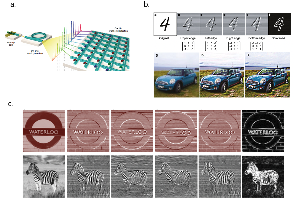
In Figure 12, parallel, fast, and efficient convolution operations are realized by a photonic tensor core [15], which is enabled by technologies such as phase change material (PCM), soliton microcombs, SiN micro-resonator, and wavelength division multiplexing (WDM) etc. The tensor core can be considered as the optical analogue of an ASIC and it achieves highly parallelized photonic in-memory computing using PCM memory arrays and photonic chip-based optical frequency combs. The computation is reduced to measuring the optical transmission of reconfigurable and non-resonant passive components and can operate at a bandwidth exceeding fourteen GHz, limited only by the speed of the modulators and photodetectors. This work reported the tensor core operating at the speed of two tera-MAC operations per second (tera = a trillion). Another key feature of this work is that, because the convolutional operation is a passive transmission measurement, the calculations can in theory be performed at the speed of light at very low power (17 fJ per MAC), experimentally limited only by the modulation and detection bandwidths. Finally, given recent advances in hybrid integration of soliton microcombs at microwave line rates, ultralow-loss Si3N4 waveguides, and high-speed on-chip detectors and modulators, this novel paradigm provides a path towards fully CMOS wafer-scale integration of the photonic tensor core with silicon photonics.
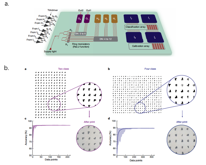
In Figure 13, the PDNN paper [19] demonstrated the first end-to-end PDNN photonic classifier chip that performs sub-nanosecond image classification through computation by propagation of optical waves, eliminating the need for an image sensor, digitization and large memory modules. PDNN directly processes the optical waves impinging on the on-chip pixel array as they propagate through layers of neurons. In each neuron, linear computation is performed optically and the non-linear activation function is realized opto-electronically, allowing a classification time of under 570 ps, which is comparable with a single clock cycle of state-of-the-art digital platforms. First, an array of 500-μm-long PIN current-controlled attenuators is used to individually adjust the optical power in each input nanophotonic waveguide of the neuron. By forward biasing the PIN junction and injecting carriers, the power of the optical wave (that is, the signal weight) of each neuron input can be adjusted. To add the weight-adjusted signals, the outputs of attenuators are photodetected using SiGe photodiodes (PDs) and the resulting photocurrents are combined to generate the weighted sum of the neuron inputs. A uniformly distributed supply light provides the same per-neuron optical output range, allowing scalability to large-scale PDNNs. Two-class and four-class classification of handwritten letters with accuracies higher than 93.8% and 89.8%, respectively, is successfully demonstrated. Particularly, low energy consumption and ultra-low computation time offered by this photonic classifier chip can revolutionize applications such as event-driven and salient object detection in autonomous driving, both as a stand-alone classifier or in conjunction with electronic processors, benefiting from the sub-nanosecond classification of the PDNN chip.
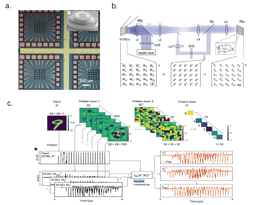
In Figure 14, the VCSEL-ONN paper [17] experimentally demonstrates a spatial-temporal-multiplexed ONN system that simultaneously overcomes all the challenges faced by other ONNs: low electro-optic conversion rate, large device footprint, and long latency. This paper exploits neuron encoding with volume-manufactured micrometer-scale vertical-cavity surface-emitting laser (VCSEL) arrays that exhibit efficient electro-optic conversion (< 5 attojoules per symbol with a -phase-shift voltage of V = 4 mV) and compact footprint (< 0.01 per device). Homodyne photoelectric multiplication allows matrix operations at the quantum-noise limit and detection-based optical nonlinearity with instantaneous response. The VCSEL-ONN architecture consists of a sequence of N layers, where each layer computes a matrix-vector multiplication followed by a nonlinear activation function. This scheme imitates the ‘axon-synapse-dendrite’ architecture in biological neurons. VCSEL-ONN encodes the input vector in i time steps to the amplitude or phase of a coherent laser oscillator (labelled ‘axon’), whose beam is dendritically fanned out to j copies for parallel processing. With three-dimensional neural connectivity, this system can reach an energy efficiency of 7 femtojoules per operation with a compute density of 6 , representing 100-fold and 20-fold improvements, respectively. The benchmarking of digit classification on MNIST dataset achieved an accuracy of 93.1% (over 98% of ground truth). Such a system is expected to run multiply-accumulate operations with an efficiency of 50 aJ/OP, limited by the memory access rather than optical energy consumption. The authors believe that optoelectronic processors with orders-of-magnitude improvement may enable us to continue the scaling of computing power in the post-Moore’s law age.
6 Recent Advances in Nanophotonics for Neuromorphic Computing
6.1 Exploration of emerging topological insulators and their potential impact
Nanophotonic technologies are leading the way in scientific and engineering progress, offering innovative approaches to observe the world through precise control of light at the nanoscale. In the wake of the seminal discovery of the quantum Hall effect, the scientific community has embarked on a journey marked by significant advancements in the realm of topological insulators (TI). For instance, in the presence of a magnetic field within the microwave frequency range, researchers observed the unidirectional transmission of electromagnetic fields, revealing their remarkable anti-scattering characteristics and robustness [158]. This unique attribute renders topological insulators exceptionally suitable for the development of nanophotonic devices. Simply put, TI enhances the fault tolerance of small-scale on-chip integrated optical systems, while enabling functionalities that were previously challenging to attain with conventional optical components.
Recently, the emergence of topological photonics marks a profound departure from conventional optical paradigms, introducing the concept of "topological invariants" and "topologically protected state" to the domain of optics. This innovative approach delves into the intriguing premise that wave functions of electromagnetic fields remain impervious to alteration amidst fluctuating geometric structures. Consequently, topological photonic devices began to widely emerge, distinguished by their exceptional optical performance attributes. These include an inherent robustness, a remarkable capacity to resist interference, the effective suppression of photon backscattering, and the realization of a notably high free spectral range (FSR).
The deliberate construction of artificial structures at strategic positions within the electromagnetic field has yielded an array of distinct optical topological states. This diverse spectrum encompasses topological bulk states[160] boundary states[161], vortex states[162], and corner states [163], each possessing unique properties. The rich collection of topological states/modes offers a diverse pool of customized photonic components, each meticulously tailored to fulfill specific functionalities. This new chapter of topological photonics, with its manifold states and promising applications, stands as a noteworthy subject of review and exploration, inviting a comprehensive examination of its significance and potential implications in the realm of optics and integrated photonics.
Within Hermitian topological systems, valley photonic crystals were used to achieve lossless topological photonic crystal waveguides, even when subjected to sharp bends [164]. Furthermore, researchers delved into the exceptional properties of topological photonic crystals when applied to slow-light waveguides [165] and polarization beam splitters [166]. Topological photonic components also can be integrated into a CMOS-compatible silicon-on-insulator (SOI) platform[167], exemplifying the immense potential of topological photonics within the field of nanophotonic.
In non-Hermitian systems, nanoscale topological photonic crystals, due to their remarkable robustness and anti-scattering properties, show great potential in lasers technology. By harnessing the unique characteristics of boundary states, bulk states, corner states (Fgure 15a), and other features inherent to topological photonic crystals, light sources with diverse optical properties can be realized [168, 160, 163, 159]. The topological photonic crystals at Dirac point brings distinct property of zero refractive index, and combined with the transmission property of topological photonic crystals, a kind of vortex state lasers can be design by precisely controlling the phase of the electromagnetic field [124, 169] (Figure 15b). This breed of laser, allowing for meticulous control of the light field distribution at the nanoscale, boasts an impressively high free spectral range and surface emission characteristics, thus emerging as a highly efficient laser source. To facilitate the transition of topological photonics into practical applications, researchers conceived topological quantum cascade lasers powered by terahertz waves, thereby significantly amplifying the potential of topological photonics across diverse research domains [170, 171].
In summary, topological photonics empowers us with the fine-grained manipulation of light fields on a smaller scale, rendering it suitable for applications in photonics-on-a-chip, optical computing, lasers, and a multitude of other pivotal domains. This advancement propels the field of nanophotonics towards even greater horizons in neuromorphic computing.
6.2 Exploration of emerging PCSELs and their potential impact
Photonic Crystal Surface Emitting Lasers (PCSELs) [113, 172, 173] (Figure 16) are a type of laser that combines the advantages of photonic crystals (PhCs) [174] and Vertical Cavity Surface Emitting Lasers (VCSELs) [175]. PhCs are artificially engineered structures with periodic changes in refractive index in one, two, or three dimensions, creating a bandgap that restricts the propagation of light in specific frequency ranges. VCSELs are lasers that emit light perpendicular to the surface of a semiconductor, facilitating efficient coupling with optical fibers and other optical components. PCSELs merge these technologies to create lasers with multiple benefits compared to traditional lasers, offering the best of both worlds.
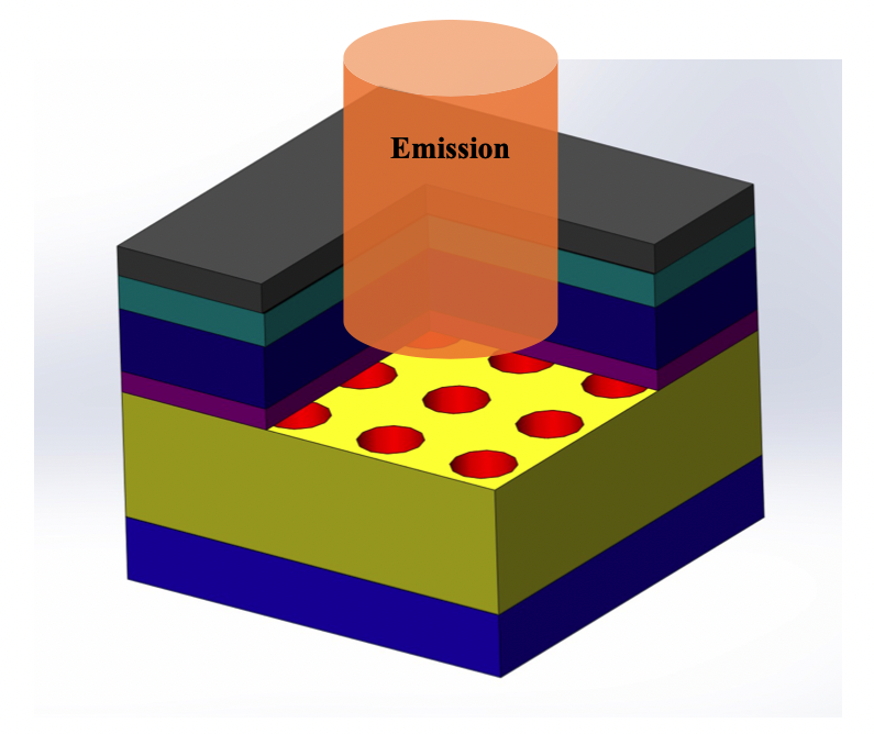
The fundamental structure of a PCSEL includes a PhC layer, an active layer, additional cladding layers, substrates, p-n junctions, and electrodes at the ends. The PhC layer mainly functions as a resonant cavity, while the active layer, typically composed of III-V materials (such as InP/InGaP, GaAs/InGaAs/AlGaAs, GaN/InGaN, etc.), is positioned in the middle of the PCSEL to induce laser emission when a population inversion of charge carriers is achieved upon reaching a certain threshold [176, 113]. Population inversion occurs when there are more electrons in higher energy states than in lower energy states, allowing for stimulated emission of photons when an electrical current is applied. When an electrical pumping current is introduced into the active layer material, it emits laser light that is effectively confined and amplified within the resonance cavity. Furthermore, the active layer can contain quantum dots or quantum wells, which increase the recombination rate of spontaneous emission, significantly enhancing the lasing effect. Consequently, PCSELs have superior characteristics than conventional VCSELs.
| VCSEL | PCSEL |
|---|---|
| Higher-order mode present | Single-model |
| Limited lasing area | Broad lasing area |
| Limited output power (mw - w) | High output power (100 w - 1000 w) |
| Large divergence angle | Narrow divergence angle |
| Non-circular light beam | Circular light beam |
Table 2 compares PCSELs to VCSELs, showcasing PCSEL’s unique advantages. Therefore PCSELs have great potential to replace those VCSEL arrays used in [17] to perform fast MAC calculations and accurate neural inference. In addition, PCSELs have a variety of applications in different fields, including:
Data Communication: PCSELs can be used in high-speed data communication systems, including optical interconnects and data centers, due to their ability to efficiently couple with optical fibers and transmit data over long distances.
Lidar Systems: PCSELs are used in Light Detection and Ranging (LiDAR) systems for applications like autonomous vehicles and 3D mapping, providing coherent and directional light sources for accurate distance measurement and object detection.
Optical Clocks and Timekeeping: PCSELs play a role in optical atomic clocks, contributing to the development of highly accurate and stable timekeeping devices used in scientific research and global positioning systems (GPS).
Quantum Technologies: PCSELs are part of quantum technologies, including quantum cryptography and quantum computing, where they provide the necessary light sources for quantum key distribution and quantum information processing.
Semiconductor Manufacturing: PCSELs are used in semiconductor manufacturing for processes like photolithography, where precise laser sources are needed for creating integrated circuits and other semiconductor devices.
Based on these applications, we see that PCSELs have the potential to drive the development of neuromorphic systems by acting as core light sources.
7 Remaining challenges and Future Directions
7.1 Strategies for improving device performance, scalability, and reliability
As neuromorphic technology continues to advance and demands are getting higher, the performance, scalability, and reliability of nanophotonic devices become increasingly critical. Achieving higher efficiency, speed, and functionality is essential to meet the ever-growing demands of modern computing tasks. This section (Table 3) will address recent developments and strategies implemented to enhance device performance, scalability, and reliability in neuromorphic photonics, where engineers and scientists are exploring a multitude of strategies. These encompass device engineering techniques, the incorporation of novel materials, and advancements in manufacturing processes. These strategies are integral in fields as diverse as semiconductor optoelectronics, photonics, and integrated systems.
| Performance | Scalability | Reliability |
|---|---|---|
| Advanced Transistor Architectures: The introduction of novel transistor architectures, such as FinFETs and gate-all-around (GAA) nanosheets, has significantly improved the performance of microprocessors. These designs offer enhanced control of the current flow, reduced leakage, and higher switching speeds [177]. | Photonic Integrated Circuits (PICs): PICs have emerged as a key strategy to integrate multiple optical modules onto a single chip, reducing size and increasing functionality [178]. Advances in PIC design and fabrication have improved the performance of devices like optical transceivers and lasers. | Redundancy and Error Correction: in electronic systems, redundancy and error correction techniques are employed to improve reliability. These methods ensure that even in the presence of defects or failures, the system continues to function correctly [179]. |
| High-Mobility Materials: The integration of high-mobility materials, like gallium nitride (GaN) and indium gallium arsenide (InGaAs), has led to faster and more efficient electronic devices. GaN power devices, for example, have found applications in power electronics and RF amplifiers [180]47. | Meta-surfaces: Meta-surfaces consist of subwavelength nanostructures that manipulate light in novel ways. These structures are integral in creating flat optical components, enabling highly compact and scalable photonic devices [181, 182]. | Reliability Testing: Rigorous reliability testing, including accelerated life tests, is conducted to identify and mitigate potential failure modes. This process ensures that devices meet their specified lifetime and performance criteria. [183] |
| Quantum Devices: Quantum devices, such as quantum-dot transistors and quantum cascade lasers, offer unique properties that can revolutionize electronics and photonics. Quantum computing, for example, has the potential to solve complex problems at unprecedented speeds [184, 185]. | Other approaches that improve the scalability… | Other approaches that improve the reliability… |
7.2 Ideas for fabrication advancements, remaining challenges, and future directions of neuromorphic photonics
In the quest for better performance, scalability, and reliability, manufacturing/fab processes also play a pivotal role and should be the focus of neuromorphic and semiconductor researchers now and in the immediate future. Table 4 lists some potential directions for manufacturing advancements, as well as some additional challenges to be solved and future directions to explore and improve.
| Manufacturing Advancements | Challenges and Future Directions |
|---|---|
| Additive Manufacturing: Additive manufacturing, including 3D printing, allows for the rapid and cost-effective production of complex components. It has applications in aerospace, healthcare, and customized electronic packaging [186, 187]. | Power Efficiency: Enhancing power efficiency remains a significant challenge. Reducing power consumption is crucial, particularly in mobile devices and data centers. |
| Monolithic 3D Integration: Monolithic 3D integration is a disruptive manufacturing technique that enables the stacking of active devices in the vertical direction (also known as epitaxy), enhancing performance and reducing interconnect lengths [188, 189, 190, 191]. | Quantum Limitations: While quantum devices show immense promise, they also present challenges such as decoherence and error correction. |
| Sustainability: The electronics industry faces questions of sustainability and responsible sourcing of materials, which are central to improving the reliability and longevity of devices. The photonics industry should avoid the same pattern. | |
| Security: As devices become more connected, ensuring the security and privacy of data remains a critical concern [192]. |
8 Conclusion
Advances in photonics have catalyzed a transformation in computational technologies, with the integration of optoelectronics onto photonic platforms leading the charge. This integration has facilitated the emergence of PICs, which act as the building blocks for ultra-fast artificial neural networks and are pivotal in the creation of next-generation computational devices. These devices are engineered to address the intensive computational demands of machine learning and AI applications across sectors including healthcare diagnostics, complex language processing, telecommunications, high-performance computing, and immersive virtual environments.
Despite the advancements, conventional electronic systems exhibit limitations in speed, signal interference, and energy efficiency. Neuromorphic photonics, characterized by its ultra-low latency, emerges as a groundbreaking solution, carving out a new trajectory for the advancement of AI and ONNs. This review casts a spotlight on the latest developments in the field of neuromorphic photonic systems from the perspective of photonic engineering and material science, critically analyzing the emergent and anticipated challenges, and mapping out the scientific and technological innovations necessary to surmount these obstacles.
The focus is on an array of neuromorphic photonic AI accelerators, examining the spectrum from classical optics to sophisticated PIC designs. It scrutinizes their operational efficiency, particularly in terms of operations per watt, through a detailed comparative analysis emphasizing key technical parameters. The discussion pivots to specialized technologies such as VCSEL/PCSEL and frequency microcomb-based accelerators, accentuating the latest innovations in photonic modulation and wavelength division multiplexing for effective neural network training and inference.
Acknowledging the current technological barriers in achieving computational efficiencies at the PetaOPs/Watt threshold, the review explores prospective strategies to enhance these critical performance metrics. These include the emerging topological insulators and PCSELs as well as strategies to advance fabrication, system scalability and reliability. The exploration aims to not only chart the current landscape but also to forecast the trajectory of neuromorphic photonics in pushing the frontiers of AI capabilities in the near future.
Acknowledgement
This work is supported by National Natural Science Foundation of China under Grant No.62174144; Shenzhen Fundamental Research Fund under Grant No.JCYJ20210324115605016 and No.JCYJ20210324120204011; Shenzhen Key Laboratory Project under Grant No.ZDSYS201603311644527; Longgang Key Laboratory Project under Grant No.ZSYS2017003 and No.LGKCZSYS2018000015; Longgang Matching Support Fund No.CXPTPT-2017-YJ-002 and No.201617486; Shenzhen Research Institute of Big Data; President’s Fund (PF01000154); and the Optical Communication Core Chip Research Platform. The authors would like to thank the engineers at the Core Research Facilities (CRF) of SUSTech for their technical support. The authors’d like to thank staff members at ITSO of CUHKSZ for their persistent support for our high-performance computing needs. The authors’d like to thanks Mr. Ceyao Zhang and Dr. Feng Yin for their fruitful discussion on ML and LLMs, and thank Mr. Qi Xin and Mr. Ping Sun for their fantastic art drawings and CAD modellings, and thank Dr. Hongjie Wang and Mr. Xiaolei Shen for their mentorship and revision tips.
Conflict of interests
The authors declare no conflict of interests.
Author contributions
Z.Z conceived and proposed the writing project. R.L. and Z.Z. designed the structure and outline of the paper. R.L. led and arranged the writing of the whole paper. R.L., Y.G., H.H., Y.Z., S.M. wrote the paper together. C.C.H. and Z.Z. supervised and mentored the project. Z.Z. managed and funded the project.
References
- [1] Stuart Russell and Peter Norvig “Artificial Intelligence: A Modern Approach” Prentice Hall, 2010
- [2] Jason Wei et al. “Emergent abilities of large language models” In arXiv preprint arXiv:2206.07682, 2022
- [3] Jianshi Tang et al. “Bridging biological and artificial neural networks with emerging neuromorphic devices: fundamentals, progress, and challenges” In Advanced Materials 31.49 Wiley Online Library, 2019, pp. 1902761
- [4] Navnidhi K Upadhyay et al. “Emerging memory devices for neuromorphic computing” In Advanced Materials Technologies 4.4 Wiley Online Library, 2019, pp. 1800589
- [5] Felipe Torres, Ali C Basaran and Ivan K Schuller “Thermal management in neuromorphic materials, devices, and networks” In Advanced Materials Wiley Online Library, 2023, pp. 2205098
- [6] Catherine D Schuman et al. “Opportunities for neuromorphic computing algorithms and applications” In Nature Computational Science 2.1 Nature Publishing Group US New York, 2022, pp. 10–19
- [7] Bhavin J Shastri et al. “Photonics for artificial intelligence and neuromorphic computing” In Nature Photonics 15.2 Nature Publishing Group UK London, 2021, pp. 102–114
- [8] Ian AD Williamson et al. “Reprogrammable electro-optic nonlinear activation functions for optical neural networks” In IEEE Journal of Selected Topics in Quantum Electronics 26.1 IEEE, 2019, pp. 1–12
- [9] Mario Miscuglio et al. “All-optical nonlinear activation function for photonic neural networks [Invited]” DOI: 10.1364/ome.8.003851MAG ID: 2900709571 In Optical Materials Express 8.12, 2018, pp. 3851–3863 DOI: 10.1364/ome.8.003851
- [10] George Mourgias-Alexandris et al. “An all-optical neuron with sigmoid activation function.” DOI: 10.1364/oe.27.009620MAG ID: 2923894441 In Optics Express 27.7, 2019, pp. 9620–9630 DOI: 10.1364/oe.27.009620
- [11] Ying Zuo et al. “All-optical neural network with nonlinear activation functions” In Optica 6.9, 2019, pp. 1132 DOI: 10.1364/OPTICA.6.001132
- [12] Tyler W Hughes, Momchil Minkov, Yu Shi and Shanhui Fan “Training of photonic neural networks through in situ backpropagation and gradient measurement” In Optica 5.7 Optica Publishing Group, 2018, pp. 864–871
- [13] Xing Lin et al. “All-optical machine learning using diffractive deep neural networks” In Science 361.6406 American Association for the Advancement of Science, 2018, pp. 1004–1008 DOI: 10.1126/science.aat8084
- [14] Yichen Shen et al. “Deep learning with coherent nanophotonic circuits” In Nature Photonics 11.77 Nature Publishing Group, 2017, pp. 441–446 DOI: 10.1038/nphoton.2017.93
- [15] Johannes Feldmann et al. “Parallel convolutional processing using an integrated photonic tensor core” In Nature 589.7840 Nature Publishing Group UK London, 2021, pp. 52–58
- [16] Xingyuan Xu et al. “11 TOPS photonic convolutional accelerator for optical neural networks” In Nature 589.7840 Nature Publishing Group UK London, 2021, pp. 44–51
- [17] Zaijun Chen et al. “Deep learning with coherent VCSEL neural networks” In Nature Photonics 17.8 Nature Publishing Group UK London, 2023, pp. 723–730
- [18] Che Liu et al. “A programmable diffractive deep neural network based on a digital-coding metasurface array” In Nature Electronics 5.2 Nature Publishing Group UK London, 2022, pp. 113–122
- [19] Farshid Ashtiani, Alexander J Geers and Firooz Aflatouni “An on-chip photonic deep neural network for image classification” In Nature 606.7914 Nature Publishing Group UK London, 2022, pp. 501–506
- [20] Demetri Psaltis, David Brady, Xiang-Guang Gu and Steven Lin “Holography in artificial neural networks” In Nature 343.6256 Nature Publishing Group UK London, 1990, pp. 325–330
- [21] Johannes Feldmann et al. “All-optical spiking neurosynaptic networks with self-learning capabilities” In Nature 569.7755 Nature Publishing Group UK London, 2019, pp. 208–214
- [22] Yitong Chen et al. “All-analog photoelectronic chip for high-speed vision tasks” In Nature Nature Publishing Group UK London, 2023, pp. 1–10
- [23] Hatice Altug, Sang-Hyun Oh, Stefan A. Maier and Jiří Homola “Advances and applications of nanophotonic biosensors” In Nature Nanotechnology 17.11 Nature Publishing Group, 2022, pp. 5–16 DOI: 10.1038/s41565-021-01045-5
- [24] Kan Yao and Yuebing Zheng “Nanophotonics and machine learning: concepts, fundamentals, and applications”, Springer series in optical sciences Cham: Springer, 2023 DOI: 10.1007/978-3-031-20473-9
- [25] Tianyu Wang et al. “An optical neural network using less than 1 photon per multiplication” In Nature Communications 13.11 Nature Publishing Group, 2022, pp. 123 DOI: 10.1038/s41467-021-27774-8
- [26] Xingyuan Xu et al. “11 TOPS photonic convolutional accelerator for optical neural networks.” DOI: 10.1038/s41586-020-03063-0MAG ID: 3118265437PMID: 33408378 In Nature 589.7840, 2021, pp. 44–51 DOI: 10.1038/s41586-020-03063-0
- [27] Bo Wu et al. “Low-threshold all-optical nonlinear activation function based on Ge/Si hybrid structure in microring resonator” DOI: 10.1364/ome.447330MAG ID: 4210275959 In Optical Materials Express, 2022 DOI: 10.1364/ome.447330
- [28] Rubab Amin et al. “0.52 V mm ITO-based Mach-Zehnder modulator in silicon photonics” In Apl Photonics 3.12 AIP Publishing, 2018
- [29] Shuming Jiao et al. “All-optical logic gate computing for high-speed parallel information processing” In Opto-Electronic Science 1.9 Opto-Electronic Science, 2022, pp. 220010–22 DOI: 10.29026/oes.2022.220010
- [30] Hongyu Hu, Xiang Zhang and Shuai Zhao “High-speed all-optical logic gate using QD-SOA and its application” In Cogent Physics 4.1 Cogent OA, 2017, pp. 1388156 DOI: 10.1080/23311940.2017.1388156
- [31] Joo-Youp Kim, Jeung-Mo Kang, Tae-Young Kim and Sang-Kook Han “All-Optical Multiple Logic Gates With XOR, NOR, OR, and NAND Functions Using Parallel SOA-MZI Structures: Theory and Experiment” In Journal of Lightwave Technology 24.9 IEEE, 2006, pp. 3392
- [32] Renjie Li et al. “Deep reinforcement learning empowers automated inverse design and optimization of photonic crystals for nanoscale laser cavities” In Nanophotonics 12.2 De Gruyter, 2023, pp. 319–334
- [33] Che Liu et al. “A programmable diffractive deep neural network based on a digital-coding metasurface array” In Nature Electronics 5.22 Nature Publishing Group, 2022, pp. 113–122 DOI: 10.1038/s41928-022-00719-9
- [34] Xuhao Luo et al. “Metasurface-enabled on-chip multiplexed diffractive neural networks in the visible” In Light: Science & Applications 11.11 Nature Publishing Group, 2022, pp. 158 DOI: 10.1038/s41377-022-00844-2
- [35] Dawn TH Tan “Topological silicon photonics” In Advanced Photonics Research 2.9 Wiley Online Library, 2021, pp. 2100010
- [36] Guo-Jing Tang et al. “Topological Photonic Crystals: Physics, Designs, and Applications” In Laser & Photonics Reviews 16.4, 2022, pp. 2100300 DOI: 10.1002/lpor.202100300
- [37] Hongwei Wang et al. “Asymmetric Topological Valley Edge States on Silicon-On-Insulator Platform” In Laser & Photonics Reviews 16.6, 2022, pp. 2100631 DOI: 10.1002/lpor.202100631
- [38] Hongwei Wang et al. “Ultracompact topological photonic switch based on valley-vortex-enhanced high-efficiency phase shift” In Light: Science & Applications 11.11 Nature Publishing Group, 2022, pp. 292 DOI: 10.1038/s41377-022-00993-4
- [39] Mohammed A Zidan, John Paul Strachan and Wei D Lu “The future of electronics based on memristive systems” In Nature electronics 1.1 Nature Publishing Group UK London, 2018, pp. 22–29
- [40] Xiaohe Huang, Chunsen Liu, Yu-Gang Jiang and Peng Zhou “In-memory computing to break the memory wall” In Chinese Physics B 29.7 IOP Publishing, 2020, pp. 078504
- [41] Shady Agwa and Themis Prodromakis “Digital In-Memory Stochastic Computing Architecture for Vector-Matrix Multiplication” In Frontiers in Nanotechnology 5 Frontiers, pp. 1147396
- [42] Charles E Leiserson et al. “There’s plenty of room at the Top: What will drive computer performance after Moore’s law?” In Science 368.6495 American Association for the Advancement of Science, 2020, pp. eaam9744
- [43] Nam Sung Kim, Deming Chen, Jinjun Xiong and W Hwu Wen-mei “Heterogeneous computing meets near-memory acceleration and high-level synthesis in the post-moore era” In IEEE Micro 37.4 IEEE, 2017, pp. 10–18
- [44] Shuo Xue “Overview of Computer Architecture Development Direction Breaking Through Von Neumann Architecture” In International Core Journal of Engineering 7.8 Boya Century Publishing Limited, 2021, pp. 330–334
- [45] Mitchell A Nahmias et al. “Photonic multiply-accumulate operations for neural networks” In IEEE Journal of Selected Topics in Quantum Electronics 26.1 IEEE, 2019, pp. 1–18
- [46] John Backus “Can programming be liberated from the von Neumann style? A functional style and its algebra of programs” In Communications of the ACM 21.8 ACM New York, NY, USA, 1978, pp. 613–641
- [47] II Arikpo, FU Ogban and IE Eteng “Von neumann architecture and modern computers” In Global Journal of Mathematical Sciences 6.2, 2007, pp. 97–103
- [48] Onur Mutlu, Saugata Ghose, Juan Gómez-Luna and Rachata Ausavarungnirun “Processing data where it makes sense: Enabling in-memory computation” In Microprocessors and Microsystems 67 Elsevier, 2019, pp. 28–41
- [49] John Shalf “The future of computing beyond Moore’s Law” In Philosophical Transactions of the Royal Society A 378.2166 The Royal Society Publishing, 2020, pp. 20190061
- [50] Caidie Cheng et al. “In-memory computing with emerging nonvolatile memory devices” In Science China Information Sciences 64 Springer, 2021, pp. 1–46
- [51] Fahimeh Yazdanpanah, Carlos Alvarez-Martinez, Daniel Jimenez-Gonzalez and Yoav Etsion “Hybrid dataflow/von-Neumann architectures” In IEEE Transactions on Parallel and Distributed Systems 25.6 IEEE, 2013, pp. 1489–1509
- [52] Mohamed Shaafiee, Rajasvaran Logeswaran and Andrew Seddon “Overcoming the limitations of von Neumann architecture in big data systems” In 2017 7th International Conference on Cloud Computing, Data Science & Engineering-Confluence, 2017, pp. 199–203 IEEE
- [53] Tianyu Wang et al. “An optical neural network using less than 1 photon per multiplication” In Nature Communications 13.1 Nature Publishing Group UK London, 2022, pp. 123
- [54] Ryan Hamerly et al. “Large-scale optical neural networks based on photoelectric multiplication” In Physical Review X 9.2 APS, 2019, pp. 021032
- [55] Cristian Neagu “Architectural exploration of Logic-in-Memory systems with DExIMA-CAD”, 2023
- [56] Carver Mead and Mohammed Ismail “Analog VLSI implementation of neural systems” Springer Science & Business Media, 1989
- [57] Wm A Wulf and Sally A McKee “Hitting the memory wall: Implications of the obvious” In ACM SIGARCH computer architecture news 23.1 ACM New York, NY, USA, 1995, pp. 20–24
- [58] Mark Horowitz “1.1 computing’s energy problem (and what we can do about it)” In 2014 IEEE international solid-state circuits conference digest of technical papers (ISSCC), 2014, pp. 10–14 IEEE
- [59] Daniele Ielmini and H-S Philip Wong “In-memory computing with resistive switching devices” In Nature electronics 1.6 Nature Publishing Group UK London, 2018, pp. 333–343
- [60] Grigory Chirkov and David Wentzlaff “Seizing the Bandwidth Scaling of On-Package Interconnect in a Post-Moore’s Law World” In Proceedings of the 37th International Conference on Supercomputing, 2023, pp. 410–422
- [61] Thomas N. Theis and H.-S. Wong “The End of Moore’s Law: A New Beginning for Information Technology” In Computing in Science & Engineering 19.2, 2017, pp. 41–50 DOI: 10.1109/MCSE.2017.29
- [62] Hassan N Khan, David A Hounshell and Erica RH Fuchs “Science and research policy at the end of Moore’s law” In Nature Electronics 1.1 Nature Publishing Group UK London, 2018, pp. 14–21
- [63] Laszlo B Kish “End of Moore’s law: thermal (noise) death of integration in micro and nano electronics” In Physics Letters A 305.3, 2002, pp. 144–149 DOI: https://doi.org/10.1016/S0375-9601(02)01365-8
- [64] Tommaso Zanotti, Francesco Maria Puglisi and Paolo Pavan “Smart logic-in-memory architecture for low-power non-von neumann computing” In IEEE Journal of the Electron Devices Society 8 IEEE, 2020, pp. 757–764
- [65] Sally A McKee “Reflections on the memory wall” In Proceedings of the 1st conference on Computing frontiers, 2004, pp. 162
- [66] Ashley Saulsbury, Fong Pong and Andreas Nowatzyk “Missing the memory wall: The case for processor/memory integration” In ACM SIGARCH Computer Architecture News 24.2 ACM New York, NY, USA, 1996, pp. 90–101
- [67] Stephen M Goodnick and Jonathan Bird “Quantum-effect and single-electron devices” In IEEE Transactions on Nanotechnology 2.4 IEEE, 2003, pp. 368–385
- [68] B Gopi, J Logeshwaran, J Gowri and V Aravindarajan “The Identification of quantum effects in electronic devices based on charge transfer magnetic field model” In NeuroQuantology 20.8, 2022, pp. 5999–6010
- [69] Xinjiang Zhang et al. “Neuromorphic computing with memristor crossbar” In physica status solidi (a) 215.13 Wiley Online Library, 2018, pp. 1700875
- [70] Ning Qiao et al. “A reconfigurable on-line learning spiking neuromorphic processor comprising 256 neurons and 128K synapses” In Frontiers in neuroscience 9 Frontiers Media SA, 2015, pp. 141
- [71] Ben Varkey Benjamin et al. “Neurogrid: A mixed-analog-digital multichip system for large-scale neural simulations” In Proceedings of the IEEE 102.5 IEEE, 2014, pp. 699–716
- [72] Shankar Ganesh Ramasubramanian et al. “SPINDLE: SPINtronic deep learning engine for large-scale neuromorphic computing” In Proceedings of the 2014 international symposium on Low power electronics and design, 2014, pp. 15–20
- [73] Ethan Farquhar, Christal Gordon and Paul Hasler “A field programmable neural array” In 2006 IEEE international symposium on circuits and systems, 2006, pp. 4–pp IEEE
- [74] Andreas Gr"̈ubl et al. “Verification and design methods for the brainscales neuromorphic hardware system” In Journal of Signal Processing Systems 92 Springer, 2020, pp. 1277–1292
- [75] Duygu Kuzum, Shimeng Yu and H-S Philip Wong “Synaptic electronics: materials, devices and applications” In Nanotechnology 24.38 IOP Publishing, 2013, pp. 382001 DOI: 10.1088/0957-4484/24/38/382001
- [76] Charles Scott Sherrington “The integrative action of the nervous system” In Scientific and Medical Knowledge Production, 1796-1918 Routledge, 2023, pp. 217–253
- [77] Eric R Kandel et al. “Principles of neural science” McGraw-hill New York, 2000
- [78] Carver Mead “Neuromorphic electronic systems” In Proceedings of the IEEE 78.10 IEEE, 1990, pp. 1629–1636
- [79] Steve B Furber, Francesco Galluppi, Steve Temple and Luis A Plana “The spinnaker project” In Proceedings of the IEEE 102.5 IEEE, 2014, pp. 652–665
- [80] Karlheinz Meier “Fast Analog Computing with Emergent Transient States in Neural Architectures, Integrated project proposal”, 2004
- [81] Todd Hylton “Systems of neuromorphic adaptive plastic scalable electronics” In DARPA SYNAPSE Bidder’s Workshop and Teaming Meeting, 2008
- [82] Qiangfei Xia et al. “Memristor- CMOS hybrid integrated circuits for reconfigurable logic” In Nano letters 9.10 ACS Publications, 2009, pp. 3640–3645
- [83] Andy Thomas et al. “Tunnel junction based memristors as artificial synapses” In Frontiers in neuroscience 9 Frontiers Media SA, 2015, pp. 241
- [84] John L Henning “SPEC CPU2000: Measuring CPU performance in the new millennium” In Computer 33.7 IEEE, 2000, pp. 28–35
- [85] Mike Davies et al. “Loihi: A neuromorphic manycore processor with on-chip learning” In Ieee Micro 38.1 IEEE, 2018, pp. 82–99
- [86] Shuiying Xiang et al. “Numerical implementation of wavelength-dependent photonic spike timing dependent plasticity based on VCSOA” In IEEE Journal of Quantum Electronics 54.6 IEEE, 2018, pp. 1–7
- [87] Simon B Laughlin and Terrence J Sejnowski “Communication in neuronal networks” In Science 301.5641 American Association for the Advancement of Science, 2003, pp. 1870–1874
- [88] Eustace Painkras et al. “SpiNNaker: A 1-W 18-core system-on-chip for massively-parallel neural network simulation” In IEEE Journal of Solid-State Circuits 48.8 IEEE, 2013, pp. 1943–1953
- [89] Luis El Srouji et al. “Photonic and optoelectronic neuromorphic computing” In APL Photonics 7.5 AIP Publishing, 2022
- [90] Ali Borji and Laurent Itti “Human vs. computer in scene and object recognition” In Proceedings of the IEEE conference on computer vision and pattern recognition, 2014, pp. 113–120
- [91] Sylvain Gelly et al. “The grand challenge of computer Go: Monte Carlo tree search and extensions” In Communications of the ACM 55.3 ACM New York, NY, USA, 2012, pp. 106–113
- [92] Chong Li et al. “The challenges of modern computing and new opportunities for optics” In PhotoniX 2.1 SpringerOpen, 2021, pp. 1–31
- [93] Jean MacMillan, Elliot E Entin and Daniel Serfaty “Communication overhead: The hidden cost of team cognition.” American Psychological Association, 2004
- [94] Danijela Marković, Alice Mizrahi, Damien Querlioz and Julie Grollier “Physics for neuromorphic computing” In Nature Reviews Physics 2.9 Nature Publishing Group UK London, 2020, pp. 499–510
- [95] Seongsik Park, Seijoon Kim, Byunggook Na and Sungroh Yoon “T2FSNN: Deep spiking neural networks with time-to-first-spike coding” In 2020 57th ACM/IEEE Design Automation Conference (DAC), 2020, pp. 1–6 IEEE
- [96] Catherine D Schuman et al. “Low size, weight, and power neuromorphic computing to improve combustion engine efficiency” In 2020 11th International Green and Sustainable Computing Workshops (IGSC), 2020, pp. 1–8 IEEE
- [97] Miao Hu et al. “Memristor crossbar-based neuromorphic computing system: A case study” In IEEE transactions on neural networks and learning systems 25.10 IEEE, 2014, pp. 1864–1878
- [98] Yi-Fan Lu et al. “Low-power artificial neurons based on Ag/TiN/HfAlOx/Pt threshold switching memristor for neuromorphic computing” In IEEE Electron Device Letters 41.8 IEEE, 2020, pp. 1245–1248
- [99] Tae Sung Lee and Changhwan Choi “Improved analog switching characteristics of Ta2O5-based memristor using indium tin oxide buffer layer for neuromorphic computing” In Nanotechnology 33.24 IOP Publishing, 2022, pp. 245202
- [100] Minghao Yan, Nicholas Meisburger, Tharun Medini and Anshumali Shrivastava “Distributed slide: Enabling training large neural networks on low bandwidth and simple cpu-clusters via model parallelism and sparsity” In arXiv preprint arXiv:2201.12667, 2022
- [101] Hsing-bung Chen and Song Fu “Parallel erasure coding: exploring task parallelism in erasure coding for enhanced bandwidth and energy efficiency” In 2016 IEEE International Conference on Networking, Architecture and Storage (NAS), 2016, pp. 1–4 IEEE
- [102] Dingbang Liu, Hao Yu and Yang Chai “Low-power computing with neuromorphic engineering” In Advanced Intelligent Systems 3.2 Wiley Online Library, 2021, pp. 2000150
- [103] Floris A Zwanenburg et al. “Silicon quantum electronics” In Reviews of modern physics 85.3 APS, 2013, pp. 961
- [104] Liang Zhang et al. “Materials, processing and reliability of low temperature bonding in 3D chip stacking” In Journal of Alloys and Compounds 750 Elsevier, 2018, pp. 980–995
- [105] Filip Ponulak and Andrzej Kasinski “Introduction to spiking neural networks: Information processing, learning and applications.” In Acta neurobiologiae experimentalis 71.4, 2011, pp. 409–433
- [106] Taojie Zhou et al. “Continuous-wave quantum dot photonic crystal lasers grown on on-axis Si (001)” In Nature communications 11.1 Nature Publishing Group UK London, 2020, pp. 977
- [107] Qianfan Xu, Bradley Schmidt, Sameer Pradhan and Michal Lipson “Micrometre-scale silicon electro-optic modulator” In nature 435.7040 Nature Publishing Group UK London, 2005, pp. 325–327
- [108] Fengnian Xia et al. “Ultrafast graphene photodetector” In Nature nanotechnology 4.12 Nature Publishing Group UK London, 2009, pp. 839–843
- [109] Massimo Cazzanelli et al. “Second-harmonic generation in silicon waveguides strained by silicon nitride” In Nature materials 11.2 Nature Publishing Group UK London, 2012, pp. 148–154
- [110] Renjie Li et al. “Deep learning-based modeling of photonic crystal nanocavities” In Optical Materials Express 11.7 Optical Society of America, 2021, pp. 2122–2133
- [111] Muhammad Aamir Iqbal et al. “Nanophotonics: fundamentals, challenges, future prospects and applied applications” IntechOpen, 2021
- [112] Renjie Li et al. “From English to PCSEL: LLM helps design and optimize photonic crystal surface emitting lasers” 14 pages, 9 graphics, 2023 DOI: 10.48550/arXiv.2104.12145
- [113] Kazuyoshi Hirose et al. “Watt-class high-power, high-beam-quality photonic-crystal lasers” In Nature photonics 8.5 Nature Publishing Group, 2014, pp. 406–411
- [114] Michael Kneissl, Andreas Knorr, Stephan Reitzenstein and Axel Hoffmann “Semiconductor nanophotonics: materials, models, and devices” Springer, 2020
- [115] Motoichi Ohtsu et al. “Nanophotonics: design, fabrication, and operation of nanometric devices using optical near fields” In IEEE Journal of Selected Topics in Quantum Electronics 8.4 IEEE, 2002, pp. 839–862
- [116] Paras N Prasad “Nanophotonics” John Wiley & Sons, 2004
- [117] Francesco Monticone and Andrea Alu “Metamaterial, plasmonic and nanophotonic devices” In Reports on Progress in Physics 80.3 IOP Publishing, 2017, pp. 036401
- [118] Alina Karabchevsky, Aviad Katiyi, Angeleene S Ang and Adir Hazan “On-chip nanophotonics and future challenges” In Nanophotonics 9.12 De Gruyter, 2020, pp. 3733–3753
- [119] Mihail C Roco et al. “Applications: nanophotonics and plasmonics” In Nanotechnology Research Directions for Societal Needs in 2020: Retrospective and Outlook Springer, 2011, pp. 417–444
- [120] Ning Xi and King Lai “Nano optoelectronic sensors and devices: nanophotonics from design to manufacturing” William Andrew, 2011
- [121] Motoichi Ohtsu, Tadashi Kawazoe, Takashi Yatsui and Makoto Naruse “Nanophotonics: application of dressed photons to novel photonic devices and systems” In IEEE Journal of Selected Topics in Quantum Electronics 14.6 IEEE, 2008, pp. 1404–1417
- [122] Daoxin Dai “Silicon nanophotonic integrated devices for on-chip multiplexing and switching” In Journal of Lightwave Technology 35.4 IEEE, 2016, pp. 572–587
- [123] Parag B Deotare et al. “High quality factor photonic crystal nanobeam cavities” In Applied Physics Letters 94.12 AIP Publishing, 2009
- [124] Jingwen Ma et al. “Room-temperature continuous-wave Dirac-vortex topological lasers on silicon” arXiv:2106.13838 [cond-mat, physics:physics] arXiv, 2021 DOI: 10.48550/arXiv.2106.13838
- [125] Biye Xie et al. “Higher-order quantum spin Hall effect in a photonic crystal” In Nature communications 11.1 Nature Publishing Group UK London, 2020, pp. 3768
- [126] Mohd Sharizal Alias et al. “Review of nanophotonics approaches using nanostructures and nanofabrication for III-nitrides ultraviolet-photonic devices” In Journal of Nanophotonics 12.4 Society of Photo-Optical Instrumentation Engineers, 2018, pp. 043508–043508
- [127] Babak Momeni et al. “Silicon nanophotonic devices for integrated sensing” In Journal of Nanophotonics 3.1 SPIE, 2009, pp. 031001
- [128] Lei Xu et al. “Scalable Networks of Neuromorphic Photonic Integrated Circuits” In IEEE Journal of Selected Topics in Quantum Electronics 28.6: High Density Integr. Multipurpose Photon. Circ. IEEE, 2022, pp. 1–9
- [129] Mohammadreza Sanadgol Nezami et al. “Packaging and interconnect considerations in neuromorphic photonic accelerators” In IEEE Journal of Selected Topics in Quantum Electronics 29.2: Optical Computing IEEE, 2022, pp. 1–11
- [130] Jonas Hansryd et al. “Fiber-based optical parametric amplifiers and their applications” In IEEE Journal of Selected Topics in Quantum Electronics 8.3 IEEE, 2002, pp. 506–520
- [131] Avinash Karanth Kodi and Ahmed Louri “Energy-efficient and bandwidth-reconfigurable photonic networks for high-performance computing (HPC) systems” In IEEE journal of selected topics in Quantum Electronics 17.2 IEEE, 2010, pp. 384–395
- [132] Snaider Carrillo et al. “Scalable hierarchical network-on-chip architecture for spiking neural network hardware implementations” In IEEE Transactions on Parallel and Distributed Systems 24.12 IEEE, 2012, pp. 2451–2461
- [133] Miltiadis Moralis-Pegios et al. “Coherent photonic neuromorphic computing for high-speed deep learning applications” In Optical Interconnects XXII 12007, 2022, pp. 25–30 SPIE
- [134] George Dabos et al. “Neuromorphic photonic technologies and architectures: scaling opportunities and performance frontiers” In Optical Materials Express 12.6 Optica Publishing Group, 2022, pp. 2343–2367
- [135] Mitchell A Nahmias et al. “Neuromorphic photonics” In Optics and Photonics News 29.1 Optica Publishing Group, 2018, pp. 34–41
- [136] Roger Dangel et al. “Polymer waveguides enabling scalable low-loss adiabatic optical coupling for silicon photonics” In IEEE Journal of selected topics in quantum electronics 24.4 IEEE, 2018, pp. 1–11
- [137] Xian Xiao et al. “Silicon photonic Flex-LIONS for bandwidth-reconfigurable optical interconnects” In IEEE Journal of Selected Topics in Quantum Electronics 26.2 IEEE, 2019, pp. 1–10
- [138] Yu Zhang, Anirban Samanta, Kuanping Shang and SJ Ben Yoo “Scalable 3D silicon photonic electronic integrated circuits and their applications” In IEEE Journal of Selected Topics in Quantum Electronics 26.2 IEEE, 2020, pp. 1–10
- [139] Xuhan Guo, Jinlong Xiang, Yujia Zhang and Yikai Su “Integrated neuromorphic photonics: synapses, neurons, and neural networks” In Advanced Photonics Research 2.6 Wiley Online Library, 2021, pp. 2000212
- [140] Jeffrey M Shainline, Sonia M Buckley, Richard P Mirin and Sae Woo Nam “Superconducting optoelectronic circuits for neuromorphic computing” In Physical Review Applied 7.3 APS, 2017, pp. 034013
- [141] Francky Catthoor, Srinjoy Mitra, Anup Das and Siebren Schaafsma “Very large-scale neuromorphic systems for biological signal processing” In CMOS Circuits for Biological Sensing and Processing Springer, 2018, pp. 315–340
- [142] Marc D Levenson, NS Viswanathan and Robert A Simpson “Improving resolution in photolithography with a phase-shifting mask” In IEEE Transactions on electron devices 29.12 IEEE, 1982, pp. 1828–1836
- [143] Arsenty Kaganskiy et al. “Advanced in-situ electron-beam lithography for deterministic nanophotonic device processing” In Review of Scientific Instruments 86.7 AIP Publishing, 2015
- [144] Manuel Gschrey et al. “Resolution and alignment accuracy of low-temperature in situ electron beam lithography for nanophotonic device fabrication” In Journal of Vacuum Science & Technology B 33.2 AIP Publishing, 2015
- [145] Jukka Viheriälä, Tapio Niemi, Juha Kontio and Markus Pessa “Nanoimprint lithography—Next generation nanopatterning methods for nanophotonics fabrication” In Recent Optical and Photonic Technologies InTech, 2010, pp. 275–298
- [146] Hongbo Lan “Soft UV Nanoimprint Lithography and Its Applications” In Updates in Advanced Lithography Rijeka: IntechOpen, 2013 DOI: 10.5772/56186
- [147] Selin HG Teo et al. “Deep reactive ion etching for pillar type nanophotonic crystal” In International Journal of Nanoscience 4.04 World Scientific, 2005, pp. 567–574
- [148] Y Fainman et al. “Silicon nanophotonic devices for chip-scale optical communication applications” In Applied Optics 52.4 Optica Publishing Group, 2013, pp. 613–624
- [149] Wolfgang Freude et al. “Design and fabrication of nanophotonic devices” In Proceedings of 2004 6th International Conference on Transparent Optical Networks (IEEE Cat. No. 04EX804) 1, 2004, pp. 4–9 IEEE
- [150] Shankar Kumar Selvaraja, Wim Bogaerts and Dries Van Thourhout “Loss reduction in silicon nanophotonic waveguide micro-bends through etch profile improvement” In Optics Communications 284.8 Elsevier, 2011, pp. 2141–2144
- [151] Thomas Campbell, Christopher Williams, Olga Ivanova and Banning Garrett “Could 3D printing change the world” In Technologies, Potential, and Implications of Additive Manufacturing, Atlantic Council, Washington, DC 3 JSTOR, 2011, pp. 1–16
- [152] Jeffrey E Melzer and Euan McLeod “3D Nanophotonic device fabrication using discrete components” In Nanophotonics 9.6 De Gruyter, 2020, pp. 1373–1390
- [153] Charles Roques-Carmes et al. “Toward 3D-printed inverse-designed metaoptics” In ACS Photonics 9.1 ACS Publications, 2022, pp. 43–51
- [154] Konstantin B Fritzler and V Ya Prinz “3D printing methods for micro-and nanostructures” In Physics-Uspekhi 62.1 IOP Publishing, 2019, pp. 54
- [155] Hoon Yeub Jeong et al. “3D and 4D printing for optics and metaphotonics” In Nanophotonics 9.5 De Gruyter, 2020, pp. 1139–1160
- [156] Jaeyeon Pyo et al. “3D printed nanophotonic waveguides” In Advanced Optical Materials 4.8 Wiley Online Library, 2016, pp. 1190–1195
- [157] Sasikanth Manipatruni et al. “Scalable energy-efficient magnetoelectric spin–orbit logic” In Nature 565.7737 Nature Publishing Group UK London, 2019, pp. 35–42
- [158] Zheng Wang, Yidong Chong, J.. Joannopoulos and Marin Soljačić “Observation of unidirectional backscattering-immune topological electromagnetic states” In Nature 461.72657265 Nature Publishing Group, 2009, pp. 772–775 DOI: 10.1038/nature08293
- [159] TJ Zhou et al. “Monolithically Integrated Ultralow Threshold Topological Corner State Nanolasers on Silicon” In ACS PHOTONICS 9.12, 2022, pp. 3824–3830 DOI: 10.1021/acsphotonics.2c00711
- [160] Zeng-Kai Shao et al. “A high-performance topological bulk laser based on band-inversion-induced reflection” In Nature Nanotechnology 15.11 Nature Publishing Group, 2020, pp. 67–72 DOI: 10.1038/s41565-019-0584-x
- [161] Tzuhsuan Ma and Gennady Shvets “All-Si valley-Hall photonic topological insulator” In New Journal of Physics 18.2 IOP Publishing, 2016, pp. 025012 DOI: 10.1088/1367-2630/18/2/025012
- [162] Xiaomei Gao et al. “Dirac-vortex topological cavities” In Nature Nanotechnology 15.1212 Nature Publishing Group, 2020, pp. 1012–1018 DOI: 10.1038/s41565-020-0773-7
- [163] Weixuan Zhang et al. “Low-threshold topological nanolasers based on the second-order corner state” In Light: Science & Applications 9.11 Nature Publishing Group, 2020, pp. 109 DOI: 10.1038/s41377-020-00352-1
- [164] Mikhail I. Shalaev et al. “Robust topologically protected transport in photonic crystals at telecommunication wavelengths” In Nature Nanotechnology 14.11 Nature Publishing Group, 2019, pp. 31–34 DOI: 10.1038/s41565-018-0297-6
- [165] Guillermo Arregui, Jordi Gomis-Bresco, Clivia M. Sotomayor-Torres and Pedro David Garcia “Quantifying the Robustness of Topological Slow Light” In Physical Review Letters 126.2, 2021, pp. 027403 DOI: 10.1103/PhysRevLett.126.027403
- [166] Lu He et al. “Topologically protected vector edge states and polarization beam splitter by all-dielectric valley photonic crystal slabs” In New Journal of Physics 23.9 IOP Publishing, 2021, pp. 093026 DOI: 10.1088/1367-2630/ac20eb
- [167] Xin-Tao He et al. “A silicon-on-insulator slab for topological valley transport” In Nature Communications 10.11 Nature Publishing Group, 2019, pp. 872 DOI: 10.1038/s41467-019-08881-z
- [168] Babak Bahari et al. “Nonreciprocal lasing in topological cavities of arbitrary geometries” In Science 358.6363 American Association for the Advancement of Science, 2017, pp. 636–640 DOI: 10.1126/science.aao4551
- [169] Lechen Yang, Guangrui Li, Xiaomei Gao and Ling Lu “Topological-cavity surface-emitting laser” In Nature Photonics 16.44 Nature Publishing Group, 2022, pp. 279–283 DOI: 10.1038/s41566-022-00972-6
- [170] Song Han et al. “Photonic Majorana quantum cascade laser with polarization-winding emission” In Nature Communications 14.1, 2023, pp. 707 DOI: 10.1038/s41467-023-36418-y
- [171] Yongquan Zeng et al. “Electrically pumped topological laser with valley edge modes” In Nature 578.77947794 Nature Publishing Group, 2020, pp. 246–250 DOI: 10.1038/s41586-020-1981-x
- [172] Masahiro Yoshida et al. “Double-lattice photonic-crystal resonators enabling high-brightness semiconductor lasers with symmetric narrow-divergence beams” In Nature materials 18.2 Nature Publishing Group UK London, 2019, pp. 121–128
- [173] Susumu Noda et al. “Photonic-crystal surface-emitting lasers: Review and introduction of modulated-photonic crystals” In IEEE Journal of Selected Topics in Quantum Electronics 23.6 IEEE, 2017, pp. 1–7
- [174] Qimin Quan, Parag B Deotare and Marko Loncar “Photonic crystal nanobeam cavity strongly coupled to the feeding waveguide” In Applied Physics Letters 96.20 American Institute of Physics, 2010, pp. 203102
- [175] Connie J Chang-Hasnain “Tunable vcsel” In IEEE Journal of Selected Topics in Quantum Electronics 6.6 IEEE, 2000, pp. 978–987
- [176] Simon M Sze, Yiming Li and Kwok K Ng “Physics of semiconductor devices” John wiley & sons, 2021
- [177] Shobhit Srivastava and Abhishek Acharya “11 Challenges and future scope of gate-all-around (GAA) transistors” In Device Circuit Co-Design Issues in FETs CRC Press, 2023, pp. 231
- [178] Carlos Errando-Herranz et al. “MEMS for photonic integrated circuits” In IEEE Journal of Selected Topics in Quantum Electronics 26.2 IEEE, 2019, pp. 1–16
- [179] Juan Manuel Peña Fernández “Error detection and diagnosis for system-on-chip in space applications”, 2022
- [180] Wendi Zhou “Fabrication and characterization of gallium nitride high electron mobility transistors” McGill University, 2013
- [181] Jie Hu, Sankhyabrata Bandyopadhyay, Yu-hui Liu and Li-yang Shao “A review on metasurface: from principle to smart metadevices” In Frontiers in Physics 8 Frontiers Media SA, 2021, pp. 586087
- [182] Dong Zhao et al. “Recent advances in ultraviolet nanophotonics: from plasmonics and metamaterials to metasurfaces” In Nanophotonics 10.9 De Gruyter, 2021, pp. 2283–2308
- [183] Patrick Girard et al. “A survey of test and reliability solutions for magnetic random access memories” In Proceedings of the IEEE 109.2 IEEE, 2020, pp. 149–169
- [184] Emanuele Pelucchi et al. “The potential and global outlook of integrated photonics for quantum technologies” In Nature Reviews Physics 4.3 Nature Publishing Group UK London, 2022, pp. 194–208
- [185] Arne Laucht et al. “Roadmap on quantum nanotechnologies” In Nanotechnology 32.16 IOP Publishing, 2021, pp. 162003
- [186] Pimal Khanpara and Sudeep Tanwar “Additive manufacturing: concepts and technologies” In A Roadmap to Industry 4.0: Smart Production, Sharp Business and Sustainable Development Springer, 2020, pp. 171–185
- [187] Mehrshad Mehrpouya et al. “The potential of additive manufacturing in the smart factory industrial 4.0: A review” In Applied Sciences 9.18 MDPI, 2019, pp. 3865
- [188] Krithika Dhananjay et al. “Monolithic 3D Integrated circuits: Recent trends and future prospects” In IEEE Transactions on Circuits and Systems II: Express Briefs 68.3 IEEE, 2021, pp. 837–843
- [189] Shuye Zhang et al. “Recent Prospectives and Challenges of 3D Heterogeneous Integration” In e-Prime-Advances in Electrical Engineering, Electronics and Energy Elsevier, 2022, pp. 100052
- [190] Zhiwen Chen, Jiaju Zhang, Shizhao Wang and Ching-Ping Wong “Challenges and prospects for advanced packaging” In Fundamental Research Elsevier, 2023
- [191] Panagiotis Chaourani “Sequential 3D Integration-Design Methodologies and Circuit Techniques”, 2019
- [192] Weixin Chen, Baoyuan Wu and Haoqian Wang “Effective backdoor defense by exploiting sensitivity of poisoned samples” In Advances in Neural Information Processing Systems 35, 2022, pp. 9727–9737