language=Verilog, basicstyle=, keywordstyle=, identifierstyle=, commentstyle=, numbers=left, numberstyle=, numbersep=10pt, tabsize=8, moredelim=*[s][\colorIndex][], literate=*::1
Theoretical Patchability Quantification for IP-Level Hardware Patching Designs
Abstract
As the complexity of System-on-Chip (SoC) designs continues to increase, ensuring thorough verification becomes a significant challenge for system integrators. The complexity of verification can result in undetected bugs. Unlike software or firmware bugs, hardware bugs are hard to fix after deployment and they require additional logic, i.e., patching logic integrated with the design in advance in order to patch. However, the absence of a standardized metric for defining “patchability” leaves system integrators relying on their understanding of each IP and security requirements to engineer ad hoc patching designs. In this paper, we propose a theoretical patchability quantification method to analyze designs at the Register Transfer Level (RTL) with provided patching options. Our quantification defines patchability as a combination of observability and controllability so that we can analyze and compare the patchability of IP variations. This quantification is a systematic approach to estimate each patching architecture’s ability to patch at run-time and complements existing patching works. In experiments, we compare several design options of the same patching architecture and discuss their differences in terms of theoretical patchability and how many potential weaknesses can be mitigated.
I Introduction
As SoC complexity continues to increase, system integrators face significant challenges in ensuring thorough design verification [1, 2]. It is difficult for system integrators to simulate and test all possible scenarios, allowing some bugs to go undetected until deployment [3, 4]. This challenge is exacerbated by time-to-market pressures, where verification teams must work under tight schedules. As bugs can be found in hardware [5, 6], software [7], or firmware [8], detecting them can require a mix of verification techniques, such as simulation, emulation, and formal approaches, which further increases the difficulty of detecting all bugs during design.
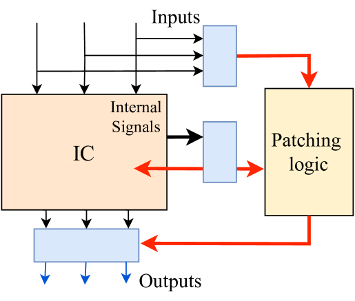
While updates can often address firmware/software bugs [9, 10], hardware bugs are typically considered as “unfixable” after deployment. To improve the resilience of systems in the field, approaches have been proposed to insert hardware-supported patching infrastructure to provide in-field patching actions [11, 12, 6, 13, 14]. However, such solutions are bespoke as it is not straightforward to compare different candidate solutions for their patching ability (which we refer to as “patchability”). In this work, we consider a patching solution that involves modifying IPs with added “patching logic” such that some signals in the design can be observed and/or modified at run-time by patching hardware, as shown in Fig. 1.
The desire for more efficient designs limits resources available for patching, thus motivating a trade-off between patchability and resource investment. This poses a major challenge for System-on-Chip (SoC) designers. Without a metric for defining patchability, system integrators must rely on their understanding of each IP and security requirements to engineer ad hoc patching designs [15]. Even if the resources available to invest in the patching architecture are determined, it is unclear which signals or registers require patching logic to achieve higher patchability. As a result, patching architectures are often suboptimal in terms of patching potential bugs.
In this work, we propose an approach to quantify the theoretical patchability of a design at Register Transfer Level (RTL) given several patch logic options. To the best of our knowledge, this is the first attempt to define patchability for patching hardware as a metric that combines notions of observability and controllability. This quantification complements prior patching work by introducing an estimate of different patching infrastructures that can be used in design trade-offs. Our contributions are as follows:
-
•
We propose a novel definition of patchability for RTL designs with integrated hardware patching logic.
-
•
We present the process to determine patchability scores for RTL designs, enabling designers to explore the effect of exposing different internal signals to patching logic.
-
•
Through the evaluation of an IP case study, our patchability scoring analysis demonstrates that our proposed approach achieves a normalized score of 0.9 while utilizing 65% fewer resources compared to a greedy approach.
II Background
We consider a patch to be a sequence of actions introduced after deployment that can mitigate an issue. We classify patches as fixes (design changes to eliminate the buggy operation) and workarounds (design changes that modify the bug’s effects, without necessarily fixing the actual cause). Software or firmware-based patches can update/fix bugs in the field, such as updating access control policy or microcode [9]. To achieve something similar for, and with hardware, hardware-based patches need hardware that is pre-designed to enable reconfiguration, i.e., inserted patching logic. Typically, a hardware patch comprises two parts: observation logic which identifies the buggy scenario and determines when to launch the corrective actions, and correction logic, which takes action to mitigate issues once notified [13, 14, 15]. A hardware-based patch requires an understanding of hardware operation and the ability to observe and control (modify) hardware signals [15].
To implement hardware patches, we consider a patching control cell as part of the patching mechanism. When selecting a signal to be directly patchable (modifiable), we substitute the original signal wire with a patching control cell (Fig. 2). To complete the patching process, the patching enable is pulled high and the patching signal is driven with the appropriate value to modify the original behavior of the signal. Patching control cells can replace inputs, outputs, internal registers, or even constant signals, to augment design elements that are already reprogrammable (e.g., control registers).

As mentioned, a patch typically comprises an observation and correction component – these determine the patchability of a patching design. Patchability, therefore, has two key features: observability and controllability. The concepts of observability and controllability have been proposed in previous work [16] and are widely used to determine a design’s testability. For clarity, we will refer to our concepts as Patching Observability (PO) and Patching Controllability (PC), respectively.
Patching Controllability (PC) refers to the extent to which a signal can be controlled by the patching logic. For a 1-bit signal, , PC is the probability that the bit can be controlled, where 0 means the bit cannot be set to a chosen value, while 1 means the bit can be set to either 1 or 0, i.e., . For an -bit signal (e.g., a bus or bit-vector), we define its PC, to be the product of the probability of controlling each bit and the number of bits in the signal, i.e., . For simplicity, we assume that all bits in an -bit signal have the same bit-level PC. Patching Observability (PO), which refers to the extent to which a signal can be observed by the patching logic, has the same formulation as PC.
For this work, we assume that all patching signals are generated using reprogrammable logic (e.g., Lookup Tables (LUTs) or some other structure such as a patching block [15]). This means that when an -bit signal is replaced by a patching control cell, the PC score is considered to be , indicating that the patch logic can change all -bits to a chosen value. This is defined as “fully controllable.”
III Patchability Formulation
This section outlines how theoretical patchability can be quantified at the RTL. As the quantification of PC and PO are mathematically equivalent, we will only focus on the calculation of PC in this paper.
| Operator | PC score |
|---|---|
| ASSIGN/NOT | |
| SHIFT | |
| OR/NOR | |
| AND/NAND | |
| XOR/XNOR | |
| CONCATENATE |
III-A Basic Operators
To analyze patchability at the RTL, we explain how the PC score is calculated given the logic of a design. We show the PC score for some common operations in RTL in Table I. For the two-input operators, and represent the PC scores of the input signals. For the single-input operator, we use to refer to the score of the input signal. For the nets that hold constant values, their PC scores are defined as 0 because we cannot control these values. We demonstrate their derivation.
OR operation (with two inputs A and B and one output out)
The probability that each input A and B (both 1-bit) is controllable is , , respectively.
Therefore, the probability that the two inputs are both controllable (assuming the signals are independently controllable) is:
| (1) |
The probability that only one input is controllable is
| (2) |
where we assume that each bit has an equal probability of being 1 and 0, e.g., for both. Thus, the probability that one bit is controllable while the other is not controllable but is the non-controlling value (e.g., 0 for OR operation) is:
| (3) |
As a result, the probability that can be controllable is the summation of Equation (1) and Equation (3), so the resulting PC score of is
| (4) | ||||
AND operation can be derived in a similar way (1 is the non-controlling value). The XOR operation does not have a controlling value. However, if one of the inputs is set to 0, the output depends on the other input. As a result, we can still obtain the same results as for OR and AND. Since we can identify the corresponding input values by observing the outputs of ASSIGN and NOT, the PC score remains the same after these two operations. The remaining PC score of other operations can be derived by using a combination of these.
III-B Conditional Assignment
Next, we discuss how to determine the PC score of conditional assignments. These examples are all 1-bit signals, and we will show more complex scenarios later. For instance, a statement where signal is conditioned on signal is shown below:
To derive the formulation of conditional assignments, we first consider a few scenarios:
If , , and are fully controllable, we can fully control .
If only & are fully controllable, we can fully control .
If only is fully controllable, we cannot fully control .
If only & are fully controllable, we can fully control .
If only or is fully controllable, we cannot fully control .
We use , , , and to represent the PC score for signals A, B, C, and D, respectively. To satisfy all the scenarios, we propose the following formulation for the conditional operator:
| (5) |
The key idea is that, given the probability that we can control the value of and thereby choose whether signal or is assigned to , we will always choose the signal that has the higher PC score (i.e., ). When we cannot control which signal to choose (with the probability ), has an equal probability to be 0 or 1 to select signals and .
If there are any constants within a conditional assignment, the PC score in Equation (5) needs to be modified. For instance, in the assignment below:
| (6) |
signals and are constants that are defined to have a PC score of . However, note that A is fully controllable if is also fully controllable. Therefore, to precisely evaluate the PC score in conditional assignments when the select signal is fully controllable (), the scores for the constants are changed to:
| (7) |
where is the number of distinct constants in the conditional block. Equation (7) quantifies the minimum number of bits that are affected by the constants. In Equation (6), two different values are present, sufficient to contribute a one-bit change of . Thus, and are 1, and therefore . This modification is also needed to compute the PC score in case statements. For example, consider
Even though signals have PC scores of zeros by definition (we cannot control any bits of them), we can fully control if is under control. In this case, all four possible 2-bit combinations can be arbitrarily assigned to through . Equation (7) helps us cover the assignments involved with constants by assigning to these constants a temporary score when calculating the resulting PC score in conditional assignments.
III-C Comparison Operator
Aside from the assignment conditioned on a signal, we often find assignments conditioned on a comparison result, e.g.,
where represents any operator that can fit in this statement, including logical operators and comparison operators, e.g., , , , . In this case, we can assume that the comparison result is assigned to signal :
where represents the probability that the condition within the parenthesis is true, and a 1-bit signal is used to represent the result. The resulting PC scores of the logical operators () are shown in Table I. Next, we explain how we derive the score of comparison operators. We first assume that all these signals are 1-bit each.
Equal to: equals can be represented in this way:
|
|
[yshift=-0.1em]belowterm1term1 \annotate[yshift=-0.1em]belowterm2term2
By combining the defined score functions of the basic operators, we obtain the score for both term 1 and term 2. By applying the OR operation of these two terms, we have:
[yshift=1.8em]abovescore1score for term1 \annotate[yshift=0.7em]abovescore2score for term2
We use logical expressions to represent these comparisons:
Greater than
Less than
Other comparisons can be derived in a similar way and we can obtain the expressions for all comparisons as .
III-D Comparison for multi-bit signals
Now, we show how to extend the single-bit comparison expressions to multi-bit signals.
Given two -bit signals and , we denote the MSB and the LSB of each as and , respectively.
A multi-bit signal comparison can be seen as a logical combination of the comparison between each bit.
For instance, the Equal comparison can be formulated as:
Equal to:
| (8) | ||||
By definition, each bit of signals and has a PC score and , respectively. By applying the corresponding functions of each operator, we obtain the score for Equation (8) as , which is the single-bit’s expressions divided by .
Greater than:
| (9) |
Since all the single-bit comparisons and basic operators have the same PC score function (i.e., ) and each bit of both signals has the same score (), the final score for Equation (9) is still . Other comparisons can be derived in a similar manner.
Note that the comparison result is always a single-bit value (True or False). Therefore, before performing the comparison between two signals, we need to divide the PC score of each signal by their widths, e.g., . This normalization process ensures that the comparison result is between and .
When the comparison is done between a signal and a value, the resulting PC score does not change. Consider the situation where we have 1-bit signals A and B. We want to see . We can take a signal B as the result of the comparison, e.g., . Because A is a 1-bit signal, this is the same saying that . For all single-bit comparison operators it should be clear that is always equal to because can take either the value of or negated.
When comparing a multi-bit signal to a fixed value, we can compare each bit of the signal with the corresponding bit of the fixed value, and combine the results to obtain the overall score. For example, to compare a 2-bit signal A:
| (10) | ||||
The PC score remains unaffected by the signal-to-value comparison. Note that it is necessary to normalize the result for maintaining consistency and allowing meaningful comparisons between different operations and evaluations.
IV Experimental Evaluation
To evaluate the proposed approach, we applied our formulation to an IP from the Hack@DAC-21 SoC [5], based on OpenPiton [17]. We assess our proposed method by generating multiple possible patching options, calculating the resulting PC score for each option, analyzing their resource usage, and investigating potentially patchable weaknesses. We use Verific libraries (academic license) to parse the design files, capture the data/information flow, and prototype a Python-based tool to calculate the resulting patchability scores with user inputs.
IV-A Selected Common Weaknesses for Evaluation
We focus on the reglk_wrapper, slightly modifying the code, as presented in Fig. 3. To assess each patching option, we selected several relevant weaknesses from MITRE’s common weakness enumerations (CWEs) and proposed example patches, determining the necessary controllable signals to address each CWE.
CWE-1262: Improper Access Control for Register Interface. Attackers can modify the internal registers due to the improper access control, which are reglk_mem entries in this case study. To patch this, we need to be able to fully control at least one of these signals: en, we, address, wdata, reglk_ctrl, or reglk_mem.
CWE-1231: Improper Prevention of Lock Bit Modification. The lock bit (reglk_ctrl) can be modified so that the access control policy is corrupted. The easiest patch is to control reglk_ctrl to mitigate this issue.
CWE-1272: Sensitive Information Uncleared Before Debug/Power State Transition. To avoid sensitive information being read by malicious users during debug mode, we can either clear the sensitive data during debug mode, or control the read transaction. Therefore, one of these signals need to be patched: reglk_mem, rdata, reglk_ctrl, address, en, rst_ni, jtag_unlock, or rst_9.
CWE-276: Incorrect Default Permissions. For example, reglk_mem should not be assigned 0s during reset. In this case, we have to control reglk_mem for patching.
IV-B Case Study
To understand how different patching options impact the patchability measure, we explore several patching strategies that select different sets of signals for patching in Table II.
| Signal Name | All Fully Patchable | Greedy In | Greedy Out | V1 In | V1 Out | V2 In | V2 Out | V3 In | V3 Out | V4 In | V4 Out | V5 In | V5 Out |
| rst_ni | 1 | 1 | 1 | 0 | 0 | 0 | 0 | 1 | 1 | 0 | 0 | 1 | 1 |
| jtag_unlock | 1 | 1 | 1 | 1 | 1 | 1 | 1 | 1 | 1 | 0 | 0 | 1 | 1 |
| rst_9 | 1 | 1 | 1 | 1 | 1 | 1 | 1 | 1 | 1 | 0 | 0 | 1 | 1 |
| we | 1 | 1 | 1 | 0 | 0 | 1 | 1 | 1 | 1 | 0 | 0 | 1 | 1 |
| address | 64 | 64 | 64 | 0 | 0 | 0 | 0 | 64 | 64 | 0 | 0 | 64 | 64 |
| wdata | 32 | 32 | 32 | 0 | 0 | 32 | 32 | 32 | 32 | 0 | 0 | 32 | 32 |
| reglk_ctrl_i | 8 | 8 | 8 | 0 | 0 | 8 | 8 | 8 | 8 | 0 | 0 | 8 | 8 |
| en_acct | 1 | 1 | 1 | 0 | 0 | 0 | 0 | 1 | 1 | 0 | 0 | 1 | 1 |
| acct_ctrl_i | 1 | 1 | 1 | 1 | 1 | 1 | 1 | 1 | 1 | 0 | 0 | 1 | 1 |
| reglk_mem[0] | 32 | 32 | 32 | 0 | 0 | 0 | 15.8 | 0 | 24 | 32 | 32 | 0 | 24 |
| reglk_mem[1] | 32 | 32 | 32 | 0 | 0 | 0 | 15.8 | 0 | 24 | 32 | 32 | 0 | 24 |
| reglk_mem[2] | 32 | 32 | 32 | 0 | 0 | 0 | 15.8 | 0 | 24 | 32 | 32 | 0 | 24 |
| reglk_mem[3] | 32 | 32 | 32 | 0 | 0 | 0 | 15.8 | 0 | 24 | 32 | 32 | 0 | 24 |
| reglk_mem[4] | 32 | 32 | 32 | 0 | 0 | 0 | 15.8 | 0 | 24 | 32 | 32 | 0 | 24 |
| reglk_mem[5] | 32 | 32 | 32 | 0 | 0 | 0 | 15.8 | 0 | 24 | 32 | 32 | 0 | 24 |
| en | 1 | 1 | 1 | 0 | 0.5 | 1 | 1 | 0 | 1 | 0 | 0 | 0 | 1 |
| reglk_ctrl | 16 | 16 | 16 | 0 | 8 | 0 | 8 | 0 | 8 | 0 | 0 | 0 | 8 |
| rdata | 32 | 0 | 32 | 0 | 0 | 0 | 11.8 | 0 | 18 | 0 | 8 | 32 | 32 |
| reglk_ctrl_o | 112 | 0 | 112 | 0 | 0 | 0 | 94.5 | 0 | 112 | 0 | 112 | 112 | 112 |
| Investment (bits) | 463 | 319 | 3 | 45 | 110 | 192 | 254 | ||||||
| Output Score (bits) | 463 | 463 | 3.5 | 253.8 | 393 | 312 | 407 | ||||||
| Normalized Score | 1 | 1 | 0.2 | 0.6 | 0.9 | 0.4 | 0.9 | ||||||
| Patchable CWEs | - | 1262, 1231, 1272, 276 | 1272 | 1262, 1231, 1272 | 1262, 1231, 1272 | 1262, 1272, 276 | 1262, 1231, 1272 | ||||||
Each patching option has In and Out columns. In shows the signals designers want to patch, and Out shows the resulting PC score after calculation. As we do not support partial control, i.e., controlling a subset of a signal, scores in In column are either 0 or equal to the signal widths (i.e., the corresponding value in All Fully Patchable column). Investment is the sum of the In scores, indicating the number of bits that are directly controlled by the patching design, and also determines the resource investment of a patching block. While the patching block’s building cost does not scale linearly with the number of bits it can patch, a higher investment leads to a larger patching block, resulting in increased resource use.
Output score is the sum of the scores in Out column, representing how many bits are controllable in a design. We divide the score in each cell of the Out column by the width of the corresponding signal, then sum up the resulting values for all signals, and finally divide the sum by the total number of signals to produce a normalized score. This score represents the average controllability per signal and accounts for different signal widths when we compare different designs.
IV-C Comparing Different Patchable Options
The greedy option makes all signals patchable except for the output, resulting in a high patchability and the highest resource investment. V1 selects some control signals that may appear helpful for patching, but they do not produce much PC to the downstream signals and are insufficient to patch many CWEs. V2 and V3 have more signals chosen for patchability, achieving normalized scores of 0.6 and 0.9, respectively. These options cost less than one-fourth of the total bits (463) and can patch up to three CWEs. Without our patchability guidance, designers might have chosen V4 to protect sensitive information by patching the reglk_mem signal. However, compared to V3, V4 costs more and achieves lower patchability scores. V5 is designed for scenarios where patching blocks can only be integrated at the interconnect level, making all signals at the interface patchable. V5 achieves similar scores to V3 but requires more bits in investment and cannot patch more CWEs than V3, demonstrating the usefulness of improving internal patchability.
Fig. 3 shows that when signals in the sensitivity list of the first always block, i.e., rst_ni, jtag_unlock, rst_9, en, we, reglk_ctrl, address, and wdata become fully controllable, arbitrary values can be assigned to reglk_mem through write transactions. Therefore, a high PC score of 24 is assigned to reglk_mem under V3’s configuration. By using the proposed formulation, we can precisely capture the relationship between signals and propagate PC scores from inputs to outputs. Previously, balancing resource usage spent on patching architectures for each target IP was challenging, given no way to quantify the resulting patchability. Our approach quantifies patchability by analyzing the structure of the design and how the data flows, making it easier to balance the resource usage while improving patchability for each block. As a result, V3 achieves a normalized score of 0.9 while utilizing 65% fewer resources compared to the greedy approach.
V Discussion
We assumed that a given CWE is considered patchable if at least one of the signals that we identified as required to be patchable is “fully” controllable. For example, even though V3 can control 24 out of 32 bits of reglk_mem, CWE-276 is still not considered patchable. However, in practice, small modifications to signals may be sufficient to prevent an attack, even if they are not fully controllable. For instance, in Fig. 3, only two bits of reglk_ctrl are used to lock registers, and these bits can be fully controlled by controlling the input signal reglk_ctrl_i. In this scenario, these two bits have different security meanings compared to other bits. Therefore, even though reglk_ctrl is only partially controllable, it can still prevent an exploit of CWE-276.
To further refine the patchability quantification formulation, it is essential to separate the controllability of signals to “0” and “1”. For instance, in Fig.3, to prevent CWE-1262 where reglk_ctrl is set incorrectly so that attackers can modify reglk_mem through write transactions, one possible patch is to control reglk_ctrl to mitigate this issue. In this case, it is only necessary to be able to set reglk_ctrl to 1 to block write transactions, and controlling it to 0 is unnecessary. Our future work will model the controllability of signals in a more granular way, separately quantifying the ability to control a signal to 0 or 1 as needed for a patch. This will allow us to quantify patchability more precisely and develop more efficient patching strategies.
Note that the choice of example CWEs in this study is independent of the patching options; in practice, each designer will anticipate potential issues in an SoC on a case-by-case basis. While we reported the number of patchable CWEs as an indicator of a patching option’s effectiveness, a high PC score does not guarantee coverage over all possible bugs. Still, we can interpret a relatively higher score when comparing different options as characterizing a design with a higher probability of successful patching. Additionally, other than using each signal’s width to represent the score, an alternative approach is to assign a security value to each signal that reflects its relative importance. This method is particularly useful when system integrators have a deep understanding of the target design and can assign appropriate security values to each signal.
While we focused on PC for brevity, PO is important in patching to capture how well a design can be monitored for misbehavior. Both PC and PO are essential components in accurately assessing a system’s patchability and developing effective patching strategies. Even though high PC and PO empower patching designs to change a design’s behavior, the security of the patching design itself is a critical consideration. Therefore, ensuring the secure delivery of patches is essential to prevent attackers from intercepting and tampering with the patch before it is received. Additionally, it is important to restrict patch creation to verified IP vendors or system integrators to prevent unauthorized access or modification.
VI Related Prior Work
Several approaches have been proposed to incorporate hardware-based patching mechanisms into SoCs for in-field IP patching. Nath et al. [14] introduced a centralized hub utilizing design-for-debug infrastructure/wrappers to monitor transactions and verify security policies at run-time. They also presented a security architecture for SoCs that involve IP communication through a Network-on-Chip (NoC) fabric [18]. Tan et al. [13] proposed decentralized patching blocks that can be reprogrammed and integrated into the IP interface. Each block stores patch programs that monitor IP behavior and override signals at the interface if buggy behavior is detected. Liu et al. [15] also proposed a decentralized patching logic and developed a formulation to help system integrators engineer the entire patching infrastructure at the system level. While prior works focus on the design of system-level patching architectures for IP design bugs and security policies, our work provides a systematic evaluation of “patchability” at the IP level. This supports system integrators in engineering the patching architecture with finer-grained assessment. The work by Guo et al. [19] quantifying information flow in hardware systems inspired us in quantifying patchability at the RTL.
VII Conclusion
This paper proposed a new approach for measuring the patchability of IP blocks. This metric helps designers compare different hardware options based on their patching controllability and observability. Our method uses probabilistic and heuristic methods to estimate controllable and observable bits in a design, considering dataflow relationships between signals. This tool can optimize patching configurations at the RTL for each IP while improving the security and reliability of hardware systems.
References
- [1] W. Chen et al., “Challenges and trends in modern SoC design verification,” IEEE Design & Test, 2017.
- [2] T. Trippel et al., “Bomberman: defining and defeating hardware ticking timebombs at design-time,” in IEEE Symposium on Security and Privacy (SP), 2021.
- [3] S. Charles, Y. Lyu, and P. Mishra, “Real-time detection and localization of distributed DoS attacks in NoC-based SoCs,” IEEE Transactions on Computer-Aided Design of Integrated Circuits and Systems, 2020.
- [4] B. Ahmad et al., “Don’t cweat it: Toward cwe analysis techniques in early stages of hardware design,” in Proceedings of IEEE/ACM International Conference on Computer-Aided Design, 2022.
- [5] G. Dessouky et al., “Hardfails: Insights into software-exploitable hardware bugs.” in USENIX Security Symposium, 2019.
- [6] L. Delshadtehrani et al., “Phmon: A programmable hardware monitor and its security use cases,” in Proceedings of USENIX Conference on Security Symposium, 2020.
- [7] A. Makhshari and A. Mesbah, “IoT bugs and development challenges,” in IEEE/ACM International Conference on Software Engineering, 2021.
- [8] S. Ray et al., “Formal verification of security critical hardware-firmware interactions in commercial SoCs,” in Proceedings of Design Automation Conference, 2019.
- [9] B. Kollenda et al., “An exploratory analysis of microcode as a building block for system defenses,” in Proceedings of ACM SIGSAC Conference on Computer and Communications Security, 2018.
- [10] K. Dharsee, E. Johnson, and J. Criswell, “A software solution for hardware vulnerabilities,” in IEEE Cybersecurity Development, 2017.
- [11] S. R. Sarangi, A. Tiwari, and J. Torrellas, “Phoenix: Detecting and recovering from permanent processor design bugs with programmable hardware,” in IEEE/ACM International Symposium on Microarchitecture, 2006.
- [12] M. Hicks et al., “Specs: A lightweight runtime mechanism for protecting software from security-critical processor bugs,” in Proceedings of International Conference on Architectural Support for Programming Languages and Operating Systems, 2015.
- [13] B. Tan et al., “Toward hardware-based IP vulnerability detection and post-deployment patching in systems-on-chip,” IEEE Transactions on Computer-Aided Design of Integrated Circuits and Systems, 2020.
- [14] A. P. D. Nath et al., “System-on-chip security architecture and CAD framework for hardware patch,” in Asia and South Pacific Design Automation Conference (ASP-DAC), 2018.
- [15] W.-K. Liu et al., “Hardware-supported patching of security bugs in hardware IP blocks,” IEEE Transactions on Computer-Aided Design of Integrated Circuits and Systems, 2022.
- [16] L. H. Goldstein and E. L. Thigpen, “Scoap: Sandia controllability/observability analysis program,” in Proceedings of Design Automation Conference, 1980.
- [17] J. Balkind et al., “Openpiton: An open source manycore research framework,” in International Conference on Architectural Support for Programming Languages and Operating Systems, 2016.
- [18] A. P. D. Nath et al., “Resilient system-on-chip designs with NoC fabrics,” IEEE Transactions on Information Forensics and Security, 2020.
- [19] X. Guo et al., “Qif-verilog: Quantitative information-flow based hardware description languages for pre-silicon security assessment,” in IEEE International Symposium on Hardware Oriented Security and Trust (HOST), 2019.