Increased light-emission efficiency in disordered InGaN through the correlated reduction of recombination rates
Abstract
Experiments have shown that the light-emission efficiency of indium gallium nitride (InGaN) light-emitting diodes improves with increasing indium concentration. It is widely thought that compositional fluctuations due to indium incorporation suppress diffusion of carriers to non-radiative centers, thus leading to defect-insensitive emission. However, recent experiments have challenged this hypothesis by revealing unexpectedly long diffusion lengths at room temperature. Here, we demonstrate an alternative mechanism involving the correlated reduction in radiative and non-radiative recombination rates that explains the increase in light-emission efficiency of InGaN with increasing indium concentration, without invoking the suppression of carrier diffusion. Our analysis challenges the notion that carrier localization gives rise to defect tolerance in InGaN.
I Introduction
Shockley-Read-Hall (SRH) recombination is a fundamental loss mechanism that impairs the energy efficiency of all light-emitting materials [1, 2]. In this process, electrons and holes recombine non-radiatively over crystalline defects to produce heat rather than recombining radiatively to produce light. The tolerance of a semiconductor to defects plays a key role in determining its suitability for light-emitting diodes (LEDs). Notably, indium gallium nitride (InGaN) LEDs exhibit remarkable brightness, even in the presence of defect densities surpassing cm-2, six orders of magnitude higher than those found in III-V arsenide and phosphide emitters [3, 4, 5, 6]. This is particularly advantageous considering InGaN serves as the most common active region in commercial visible LEDs [7].
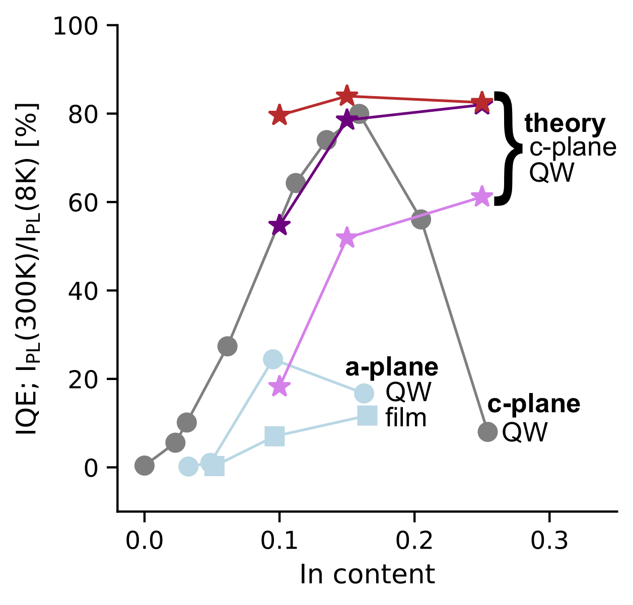
Despite their resounding success, a comprehensive understanding of the performance of nitride LEDs remains incomplete [8], limiting their advancement into longer visible and shorter ultraviolet wavelengths [9, 10] that are crucial for augmented-reality and germicidal applications. Experiments have shown that increasing the compositional disorder of InGaN increases the internal quantum efficiency (IQE), which is the ratio of the radiative recombination rate to the total recombination rate [11, 12, 13, 14, 15], as reproduced in Figure 1. (At higher indium concentrations, the IQE drops because of a degradation in the material quality.) The improvement in efficiency with indium concentration is widely used to justify the claim that alloy disorder in InGaN imbues it with some tolerance to defects. However, care must be taken in interpreting these IQE measurements, as they were obtained using techniques that do not give access to the operating carrier density in the active region. Here, we propose an alternative mechanism relating to the operating carrier density that can explain the experimentally observed increase in the IQE without the notion of defect tolerance.
According to the prevailing hypothesis, compositional fluctuations in InGaN confines carriers to randomly occurring regions of narrower band gap and higher crystal quality [16, 17, 12, 18, 19], preventing them from diffusing towards non-radiative recombination centers [11, 15, 20]. Following this reasoning, one might expect the internal quantum efficiency (IQE) of InGaN LEDs, defined as the ratio of the radiative recombination rate to the total recombination rate, to be relatively independent of defect density; however, empirical evidence contradicts this notion [21, 22, 23, 24, 25, 26, 27, 28, 29, 30, 31]. Even the hypothesis that disorder suppresses diffusion in InGaN has come under scrutiny, because a substantial fraction of carriers at room temperature are extended and able to diffuse [32]. Diffusion lengths in InGaN alloys reach tens of microns at room temperature [33, 34, 35, 36], surpassing the typical distance between defects. This poses perplexing questions: does InGaN exhibit defect tolerance and what role does disorder play?
The influence of compositional disorder on recombination in InGaN remains a subject of intense debate [37, 38, 39, 40, 41, 42, 43, 44, 45, 46, 47, 48, 49, 50, 51, 52, 53, 54, 55, 56, 57, 41, 58, 59, 60, 61, 62]. For example, the tolerance of InGaN quantum wells to threading dislocations has been explained in terms of energetic shielding of dislocation cores due to quantum confinement. While this hypothesis certainly explains why high threading dislocation densities are not catastrophically detrimental to InGaN LEDs, it fails to account for the increased efficiency of disordered bulk films with increasing composition (e.g., see a-plane film in Figure 1) [63, 64, 65]. Another hypothesis posits that phase-segregation of cations [66] prevents carriers from reaching dislocation cores, but this explanation does not account for non-radiative recombination involving point defects away from dislocations, which contribute significantly to non-radiative recombination [67]. Studying the impact of compositional disorder on recombination dynamics is challenging experimentally. The difficulty lies in independently controlling disorder while keeping other influential factors, such as growth conditions, microscopic polarization fields, and defect-transition levels, constant. On the other hand, it is much easier to control for disorder effects with predictive numerical-modeling techniques. By explicitly solving the Schrödinger equation, which governs the physics of electrons and holes, we can disentangle the impact of localization on recombination from other factors.
In this work, we investigate the claim that carrier localization is responsible for the defect-insensitive emission of InGaN. To test this hypothesis, we simply calculate what happens to the competition between radiative and SRH recombination if we change the degree of localization. By manipulating the alloy-scattering potential of the random alloy, we directly control the strength of alloy disorder and solve the Schrödinger and Poisson equations in the modified potentials. Our analysis includes hundreds of eigenstates, spanning the range from localized to extended. Our results challenge the status quo, and we find that carrier localization does not increase the ratio or the IQE for a given defect density. Instead, we propose that carrier localization slows both radiative and non-radiative recombination in a correlated manner; this increases the operating carrier density and promotes bimolecular radiative recombination over monomolecular non-radiative recombination for a given operating current density or optical illumination intensity. Therefore, we propose that the enhancement of the IQE in Figure 1 is very likely be due to differences in the carrier density with increasing carrier localization rather than due to defect tolerance. Additionally, because polarization fields in quantum wells also increase the operating carrier density, they have a similar effect in promoting radiative recombination over non-radiative recombination in c-plane quantum wells at low currents.
II Theoretical modeling of recombination
II.1 Schrödinger-Poisson calculations
To assess the influence of compositional disorder on the competition between radiative and SRH recombination, we have developed a theoretical framework based on solutions to the Schrödinger and Poisson equations. In our approach, we model alloy disorder in InGaN by randomly assigning the composition in a grid as either (GaN) or (InN). By manipulating the alloy-scattering potential, we directly control the degree of carrier localization, which allows us to probe its impact on recombination dynamics. For our calculations, we used first-principles density-functional theory to parameterize the effective-mass Hamiltonian [68, 69, 70, 71, 72, 73], which we diagonalized using nextnano++ [74], obtaining hundreds of eigenstates. We modeled periodic supercells of size 18 nm 18 nm 18 nm with a grid-size spacing (0.3 nm) that corresponds to the nearest-neighbor distance between cations in InGaN. Unless specified otherwise, we repeated each calculation for ten different configurations of the random alloy. We tuned the hole scattering potential to span the range from 0.0 eV to 1.0 eV, while fixing the electron scattering potential to the first-principles conduction-band offset energy of 2.3 eV [73]. We note that experimental measurements have determined the VB offset to be between 0.5 eV and 1.1 eV [75, 76, 77, 78, 79, 80, 81]. To better understand the meaning of the scattering potentials, it is illustrative to consider the extreme limit of a virtual-crystal alloy, for which there is no alloy-scattering potential, and .
II.2 Relation between recombination rates and wave-function overlaps
Central to our analysis is the relationship between recombination rates and the overlap of the carrier wave functions from perturbation theory. The rate of radiative recombination is proportional to the squared overlap of the electron and hole wave functions , [82, 52, 83, 84]
| (1) | ||||
| (2) |
where is the envelope wave function, is the non-degenerate occupation probability at room temperature, and the indices and correspond to conduction band (CB) and valence band (VB) states, respectively. We emphasize that the summations over and are performed over hundreds of eigenstates, including extended hole states, and we ensure that including more eigenstates in our solver does not appreciably change the overlap. Equation (2) rescales the overlap with respect to the virtual-crystal approximation (VCA) to ensure the limit for systems with translational invariance. Therefore, being greater than one means that the overall probability of spontaneous recombination is exacerbated compared to a virtual-crystal, while means that the probability is suppressed. is proportional to the radiative recombination coefficient , which relates to the rate of radiative recombination according to , where is the carrier density. The quantity is proportional to the oscillator strength, which quantifies the probability of light emission from a material.
The rate of SRH recombination is also proportional to an integral that resembles an overlap,
| (3) |
where is the ratio of a given defect’s hole and electron capture coefficients, and and are the electron and hole densities divided by the total number of carriers in the simulation volume . We provide a derivation of equation (3) in Appendix A, and discuss how the microscopic details of the atomistic physics involving carrier capture by defects, multi-phonon-emission, and details of the defect wave functions, are embedded in the parameter through the capture coefficients. The term is proportional to the SRH recombination coefficient , which in turn is related to the SRH rate according to . One can also check that for systems with translational invariance. We note that does not depend on and independently, and only depends on their ratio , representing a convenient separation of physics by length scale. Very large or very small values of indicate poor non-radiative recombination limited by the capture of either electrons or holes, respectively, meaning that these two processes are decoupled. In contrast, values of near unity indicate that a defect captures electrons and holes successively and quickly, thus the probability of recombination depends strongly on the probability of both carriers being found at the defect site at the same time. Thus, by studying how compositional disorder impacts and , we can evaluate its influence on the radiative and SRH recombination rates.
II.3 Connection to approaches that explicitly model diffusion
Since carriers need to diffuse to defects in order for them to be captured by multi-phonon emission and diffuse to each other in order for them to spontaneously recombine, one may wonder if it is necessary to explicitly model the dynamic evolution of carriers to accurately model the quantum efficiency. Fortunately, information of the time evolution of a system (in the absence of an external driving force) is embedded in its energy eigenstates [85], and the challenge is in simply extracting this information. For a system in quasi-steady-state equilibrium, the problem is simplified because the system is accurately described as a linear combination of its energy eigenstates, weighted by thermal occupation factors (in this case, determined using Fermi-Dirac statistics) [86]. In this limit, the rate of dynamic processes can be efficiently computed using Fermi’s golden rule, which involves integration of wave-function overlaps over the eigenspectra of the Hamiltonian [85, 86]. With respect to this work, it is the wave-function overlaps that contain information about whether a carrier can diffusively reach a defect. For example, a hole wave function localized away from a defect will have negligible overlap with the defect state, while a delocalized wave function that can reach the defect will have finite overlap with it. The formalism based on energy eigenstates has been successfully and widely applied to study both radiative and non-radiative processes in nitride semiconductors, using density-functional theory [87, 88], empirical tight-binding [89, 90], and Schrödinger-Poisson solvers [91, 47, 52, 92, 83, 32].
We briefly discuss the challenges present in other approaches that explicitly model the dynamic evolution of carriers, and justify our choice of employing the eigenstate formalism. The most general approach involves non-adiabatically propagating carrier populations and coherences in time, while simultaneously evolving the lattice [93]. The advantage of this method is that it is valid out of equilibrium and can capture non-adiabatic processes such as hopping of localized states. However, this approach is intractable for the problem at hand as it is limited to small supercells that do not capture carrier localization, and the required timescales would span order of magnitudes from femtoseconds for the electron-phonon interaction to nanoseconds and microseconds for recombination. Another approach couples the Schrödinger and Poisson equations (or the Localization Landscape model) with the drift-diffusion equation [94, 95, 96]. The drift-diffusion equation is derived from Boltzmann transport theory, which by design only tracks carrier populations and neglects wave coherences [97]. Applying the drift-diffusion model to the study of localized states is not justified from a theoretical standpoint because localization is fundamentally a manifestation of wave coherences due to multiple scattering [98]. One may, of course, correct the diffusion constant and mobility to account for the fact that a fraction of carriers are localized, but this is only valid if one is interested in studying average transport effects rather than the behaviour of localized carriers. From a technical perspective, most Schrödinger-Poisson-drift-diffusion models also suffer from the self-interaction problem arising from the use of the Hartree approximation [99], which artificially delocalizes wave functions, which we have observed in drift-diffusion simulations that we performed using nextnano++. In contrast, the approach based on energy eigenstates that we have adopted in this work does not suffer from these technical issues, and provides a way to accurately model the quantum efficiency under quasi-steady-steady conditions.
III Results and discussion
III.1 Localization of wave functions
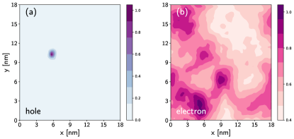
Our solutions to the Schrödinger and Poisson equations indicate that compositional disorder in InGaN leads to the localization of carrier wave functions. This localization stems from the confinement of wave functions in regions of narrower band gap as well as the interference of wave functions due to multiple scattering by the disordered potential [100]. We find that while electrons exhibit extended wave functions, holes near the valence-band maximum are strongly localized (Figure 2), consistent with atomistic tight-binding calculations [48, 101]. This asymmetry in localization arises from the difference in effective masses between electrons and holes in the III-nitrides ( and ). This finding is crucial for understanding recombination dynamics, as we discuss later. As a result of the weak impact of disorder on the electron wave function, our investigation centers on the effects of hole localization on carrier-recombination dynamics.
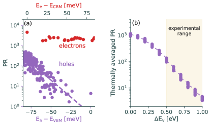
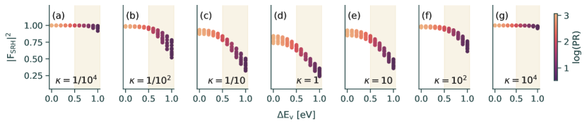
To investigate the influence of hole localization on recombination, we controlled the disorder strength by tuning the alloy-scattering potential. In our calculations, we vary the tune the hole scattering potential from 0.0 eV to 1.0 eV, while fixing the electron-scattering potential to the theoretical CB offset of 2.3 eV. To quantify the degree of localization, we employ the thermally averaged participation ratio (PR), which measures the number of sites over which the wave functions are extended. We define the PR as . According to this definition, a state localized to a single site has PR equal to the differential volume element, and a state fully extended over the simulation volume has PR equal to the simulation volume. Using scattering potentials equal to first-principles CB and VB offsets, we find that electrons are extended within the simulation cell but holes near the valence-band maximum are strongly localized, with their PR decreasing exponentially near the band edge (Figure 3(a)). Moreover, increasing the hole-scattering potential leads to stronger hole localization due to the heightened disorder strength (Figure 3(b)).
III.2 Localization reduces recombination rates
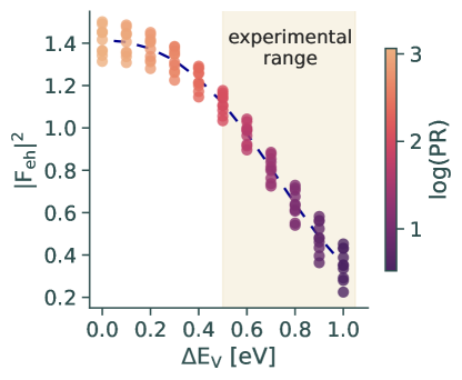
Our findings demonstrate that compositional disorder in III-nitrides leads to a decrease in the overlap of electrons and holes , primarily driven by the asymmetry in their effective masses. Figure 4 illustrates the dependence of on hole localization in In0.15Ga0.85N alloys. The reason for is that there are strain fluctuations in our simulation that reduce the symmetry of the alloy even for and enable optical transitions that are symmetry-forbidden in a virtual crystal. As holes, on average, become more localized, their spectral weight is transferred away from the point, reducing their coupling with extended electrons whose spectral weight is highly concentrated near . Figure S1 of the Supplemental Material (SM) shows that artificially localizing electrons alongside holes increases the wave-function overlap [102]. Consequently, the asymmetry in effective masses within the III-nitrides leads to a decrease in the rate of radiative recombination with stronger disorder.
On the other hand, the effect of disorder on non-radiative recombination depends on the of the defect over which recombination occurs. Figure 5 shows the influence of carrier localization on for recombination over defects with varying values. For close to unity, hole localization reduces the SRH integral by reducing the probability of finding an electron and hole at a defect site. In contrast, for extreme values of , hole localization has no effect on the SRH integral. This is because the SRH cycle is limited by multi-phonon emission rather than hole localization, as the presence of a hole at a defect site is always finite due to thermal occupation of extended states. Since defects with symmetric capture coefficients are typically the most efficient non-radiative recombination centers, overall, disorder tends to reduce the rate of SRH recombination.
III.3 Power-law scaling of radiative and SRH recombination
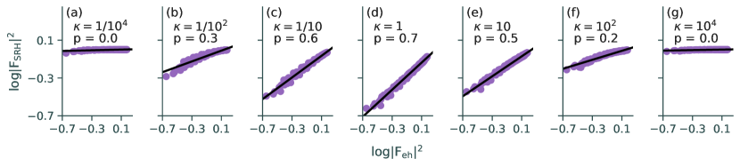
Previous studies have assumed that carrier localization only reduces the coefficient but has no impact on the coefficient [50, 52, 59]. We find that this assumption is not justified. Carrier localization reduces the rates of both radiative and SRH recombination in a correlated manner, and the correlation follows a power law of the form,
| (4) |
In Figure 6, we show this scaling relation and the power law exponent explicitly for various values of . We find the following approximate expressions for and : and . If is close to unity, the rate of non-radiative recombination is proportional to the probability of finding both an electron and hole at a defect site, therefore is proportional to . In contrast, is independent of for extremely large or extremely small values of because the rate of non-radiative recombination is limited by the carrier-capture process. In Figures S2 and S3 of the SM, we also show that assuming non-random defect distributions does not change our conclusions. The power-law relationship between radiative and non-radiative recombination, as demonstrated in our study with varying hole localization, seems to be a general feature of recombination in III-nitrides. Other authors have observed it for varying quantum-well thickness and composition, showing that polarization fields have a similar effect [92, 83, 58].
III.4 Analysis of point-defect tolerance
The IQE ultimately depends on the ratio of the radiative to the total recombination rate. We capture this competition by considering the impact of wave-function overlap on the recombination rates,
| IQE | ||||
| (5) |
Here, is the total carrier-capture coefficient by point defects calculated without localization effects, e.g., at the level of density-functional theory, is the defect density, and is the bulk radiative recombination coefficient also calculated without localization effects. and introduce corrections due to disorder or polarization fields for the case of polar quantum wells. Since we are interested in the current regime where defect-mediated SRH recombination dominates, we neglect third-order Auger-Meitner recombination (AMR) [103, 104], however we later verify that the presence of AMR does not change our conclusions using experimentally measured coefficients. We have simplified the IQE expression by rewriting the SRH integral using the power-law relation discussed in Section III.3.
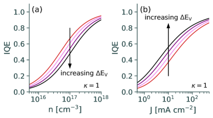
We now argue that the carrier localization does not lead to point-defect tolerance in InGaN. In order for carrier localization to give rise to defect tolerance, the IQE, at a given carrier density and a given defect density, would have to increase with stronger localization. Instead, we find that stronger localization decreases the IQE at a fixed carrier density (Figure 7(a)). To evaluate the IQE expression in equation (5), we varied from 0.1 to 1.5 and used a DFT-level recombination coefficient of . For the coefficient, we assumed a fixed defect density such that the product . The absence of defect tolerance can be understood by observing that the scaling exponent , which governs the power-law relation between radiative and SRH recombination, is always positive. Defect tolerance would require either to be negative or if equals zero then would have to increase with stronger localization. As neither condition is met, this analysis challenges that idea that InGaN is tolerant to point defects.
III.5 Why does the IQE improve with increasing indium content?
The improvement of the IQE with increasing indium concentration (Figure 1) has thus far been attributed to the enhanced defect tolerance of In-containing alloys. Can another mechanism explain this phenomenon? One possibility is that point defects do not play a significant role in SRH recombination for the measured samples, and the observed increase in the IQE can be explained completely in terms of greater energetic screening of threading dislocation cores with increasing indium concentration. We believe this scenario to be highly unlikely since first-principles calculations have shown that point defects in the nitrides will form and contribute to SRH recombination even in samples of the highest quality [67, 105, 106]. There is also increasing evidence that the majority of non-radiative losses in the active region of InGaN LEDs occurs through point defects rather than threading dislocations [26, 27, 28, 29, 30, 31].
Instead, the increase in the IQE with increasing indium concentration can be explained in terms of the fact that experiments are often performed under constant current conditions. Under constant current, higher indium-content emitters operate at higher carrier densities due to their slower recombination rates. An increase in the carrier density leads to the promotion of bimolecular radiative recombination () over monomolecular SRH recombination (), giving rise to an apparent improvement of the IQE that can be mistaken for defect tolerance. We show this phenomenon explicitly in Figure 7(b), where the IQE at a fixed current density increases with stronger localization, despite no change in the defect density. For this calculation, we assume since defects with symmetric capture coefficients tend to be the most active recombination centers but later we explicitly verify our conclusions with experimentally measured recombination coefficients, including the coefficient. (In Appendix B, we explain that our conclusions do not change in the limits or . In these limits, multi-phonon emission is inefficient and band-to-band recombination competes with radiative capture by point defects, which scale linearly with each other.) Therefore, although carrier localization decreases the quantum efficiency at a given carrier density, it increases the quantum efficiency at a given current density, which is the relevant quantity for experimental measurements. As we discuss later in the text, this is the opposite of what occurs at higher current densities in the efficiency-droop regime.
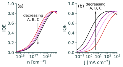
We now show that our proposed mechanism applies to commercial LEDs as well, despite the presence of additional factors such as carrier separation by polarization fields, Auger-Meitner recombination, variations in band gap and quantum-well thickness, and various types of defects contributing to non-radiative recombination. To account for these factors in our analysis, we use the empirical scaling relation between the , , and coefficients of samples of various thicknesses and compositions that are representative of commercial LEDs [58]. We note that we do not explicitly model the screening of polarization fields because their impact on recombination coefficients in the carrier-density range of interest is rather small; nevertheless, our use of scaling relations implicitly accounts for their effects on the competition between radiative and non-radiative recombination [58]. In Figure 8, we present the IQE as a function of both carrier and current density, for coefficients ranging from to . We observe that the IQE at a given carrier density decreases as the coefficient decreases, while the IQE at a given current density has the opposite behavior.
Finally, we revisit Figure 1 and explicitly calculate the IQE to show that our mechanism can explain the improvement in the IQE with increasing indium concentration. In order to compare against experiments for which the total recombination rates are not known, we calculated the IQE for various current densities (1, 10, and 100 mA/cm2). We used accurate coefficients for InGaN quantum wells that were calculated by diagonalizing atomistic tight-binding Hamiltonians parameterized to first-principles DFT calculations [90]. To obtain the and coefficients from the coefficient, we used empirical power-law relations measured for quantum-well designs that are representative of commercial LEDs [58]. Our calculations, shown in Figure 1, clearly show that the improvement in the IQE with increasing indium concentration can be explained in terms of differences in carrier density rather than suppression of diffusion to non-radiative centers by carrier localization. The differences in carrier density can occur because of stronger carrier localization or stronger polarization fields, the latter of which has a greater effect as it can influence the recombination rates by orders of magnitude. We believe that further experimental work, using differential-lifetime-based techniques that give simultaneous access to the IQE and the operating carrier density [58, 84], is warranted to verify the mechanism that we have proposed.
III.6 Consequences to devices
While reducing the overlap of carrier wave functions can enhance the IQE at low current densities, it has drawbacks for high-power device performance. At higher current densities, decreased overlap favors third-order Auger-Meitner recombination over bimolecular radiative recombination [91, 84], shifts the maximum efficiency to lower current densities, and worsens the problematic hue shift of LEDs [107]. This finding cautions against relying solely on comparisons at a single carrier-injection level if evaluating the efficiency of different devices, especially with regards to notions of defect tolerance. Moreover, it is crucial to recognize that reducing the carrier overlap overall decreases the IQE at a given carrier density, therefore the IQE is in fact highly sensitive to the defect density. This is consistent with observations that reducing the point-defect density dramatically improves the maximum IQE of compositionally disordered LEDs [26, 27, 28, 29, 30, 31]. Nevertheless, there may be applications, such as low-power microLEDs with large surface recombination velocities [108], where reducing the wave-function overlap, e.g., by promoting carrier localization or increasing the thickness of polar quantum wells, could be advantageous for improving the low-current quantum efficiency.
IV Conclusion
To conclude, we have addressed the longstanding controversy of whether compositional disorder in InGaN leads to defect tolerance. We do not find evidence that carrier localization is responsible for the highly efficient nature of InGaN, as commonly believed. A reduction in wave-function overlaps and recombination rates accompanied by an increase in the carrier density, rather than suppression of diffusion, can explain the enhancement of the light-emission efficiency with increasing indium concentration. We believe there is good motivation for further experimental work using advanced techniques that give simultaneous access to the carrier density and the recombination rates in the active region to verify this mechanism. At higher powers, the same mechanism exacerbates efficiency droop and worsens the hue shift of LEDs. Naturally, the maximum quantum efficiency depends strongly on the overall defect density regardless of the wave-function overlap, emphasizing the need to reduce defect concentrations. This work provides a theoretical framework applicable to other semiconductors for understanding the impact of disorder on recombination dynamics, paving the way for accurately assessing the impact of disorder on the performance of optoelectronic devices.
Acknowledgements
We thank Rob Armitage, Daniel Feezell, Mark Holmes, and Siddharth Rajan for useful discussions, and Kyle Bushick, Amanda Wang, and Xiao Zhang for their help editing this manuscript. This project was funded by the U.S. Department of Energy, Office of Energy Efficiency and Renewable Energy, under Award No. DE-EE0009163. Computational resources were provided by the National Energy Research Scientific Computing Center, a Department of Energy Office of Science User Facility, supported under Contract No. DEAC0205CH11231. N.P. acknowledges the support of the Natural Sciences & Engineering Research Council of Canada Postgraduate Scholarship.
Appendix A Derivation of
We can write the rate of Shockley-Read-Hall (SRH) recombination (otherwise known as non-radiative recombination by multi-phonon emission) as being proportional to a quantity that we denote . This term is not strictly an overlap term but it involves overlap-like integrals of the wave functions, therefore we interchangeably refer to it as the SRH overlap term. To derive this term, we start from the generalized SRH recombination rate that accounts for non-uniformities in the charge density,
| (6) |
where and are any given defect’s electron and hole capture coefficients, and are the spatially varying electron and hole carrier densities, and is the trap density. For this expression, we have assumed that traps are uniformly distributed, however we also explicitly verify this assumption by relaxing this assumption and allowing the trap density to vary spatially (see Figure S1 and S2 of the supplementary material).
The process of SRH recombination involves the capture of one carrier by a defect, followed by a subsequent capture of a second carrier. The atomistic defect-level physics of this phenomenon, including the multi-phonon-emission physics, is captured in the electron () and hole () capture coefficients, . The capture coefficient is defined as, [87]
| (7) |
where is the simulation volume, is a degeneracy factor, is the initial atomistic wave-function prior to carrier capture and is the wave-function captured by the defect, is the electron-phonon-coupling Hamiltonian, and index the vibrational modes of the excited electronic defect state, is a bosonic occupation factor, and are initial and final vibrational wave-functions of the defect, is the change in normal coordinates of the defect before and after multi-phonon emission, and the function conserves energy during the electronic () and vibronic transitions. In principle, and should also vary spatially as the capture rate can depend on the local alloy configuration and nearest-neighbour bonding environment. However, explicit ab initio calculations have shown that these effects average out once one considers that defects are found in a multitude of local environments, and one can accurately define effective capture coefficients for the entire crystal [105]. As we will later show, if one is only interested in the correction to the SRH rate relative to the virtual-crystal case, one only needs to know the ratio rather than the exact values of and . Hence, in our formalism, the effects of the atomistic carrier-capture and multi-phonon-emission processes are embedded in . Since can vary for different defects, we treat it as an input parameter of our theory, and vary it across a range of reasonable values from very large () to very small (). We then use our intuition that defect states with symmetric capture coefficients are most active for SRH recombination to extract conclusions for devices.
While the carrier capture coefficients describe the physics of multi-phonon-emission and defect-carrier capture, one also needs to consider the local charge densities and to evaluate the rate of SRH recombination. We construct the local charge density from the envelope functions calculated for the random alloy without defects in the supercell. The underlying assumption is that the defect states are so dilute that they do not significantly modify the charge density. Indeed, we have explicitly checked that modeling a single point defect with a localized deformation potential of order 1 eV has no discernible influence on the envelope functions. This assumption has also been used by other authors to model the SRH process in nitride quantum wells [92]. It is important to note that this assumption may not hold for the case of charged defects, whose electrostatic field will cause a local redistribution of the charge density. In the defect literature, this correction goes under the name of the Sommerfeld enhancement-factor correction, and it should either be applied to the capture coefficient or the local charge density but not both. Since it is conventional to directly apply this correction factor in the calculation of the ab initio capture coefficient [87], we have excluded its effects in our calculation of and to avoid double counting. Other researchers employing similar methods as us have noted that charging effects are not essential for capturing the correct qualitative physics of nitride emitters [92].
At this point, we perform further algebraic manipulations to rewrite . Under symmetric injection of electrons and holes, i.e., , where is the total number of carriers, we can rewrite the electron and hole densities as and , where the spatially varying parts are given by and , where and index conduction and valence bands respectively, and is the Fermi-Dirac occupation probability. Here, we stress that the summation over and occur over hundreds of eigenstates, allowing us to capture the effects of both localized and extended states. Factoring out , we can rewrite the SRH rate as,
| (8) |
For a system with translational invariance, the macroscopic charge density is spatially uniform and , thus . We define as the correction factor to the SRH recombination rate due to carrier localization effects, thus,
| (9) |
where we have defined . This is the expression that we have provided in the main text. We reiterate that the effects of the atomistic carrier capture process, included details of the multi-phonon-emission physics, defect-charging effects, and details of the atomistic defect wave functions, are embedded in the parameter.
Appendix B Impact of radiative capture by defects on the IQE
In the main text, we showed that and are almost linearly correlated for , and completely uncorrelated for and . We also showed that near-linear correlation between and leads to an apparent defect tolerance at low current densities. In the extreme limits of , multi-phonon emission becomes prohibitively slow, in which case the dominant mono-molecular recombination process that competes with band-to-band radiative recombination is radiative capture by point defects, such as the impurity in GaN. This modifies the ABC model as,
| (10) |
where is the radiative-capture recombination coefficient. Similar to the coefficient, the coefficient is also proportional to the electron-hole overlap as it is proportional to a momentum matrix element governing defect-to-band or band-to-defect transitions. Therefore, our conclusions do not change even if band-to-band recombination competes with radiative capture by point defects rather than multi-phonon emission.
References
- Shockley and Read [1952] W. Shockley and W. T. Read, Statistics of the Recombinations of Holes and Electrons, Physical Review 87, 835 (1952).
- Hall [1952] R. N. Hall, Electron-Hole Recombination in Germanium, Physical Review 87, 387 (1952).
- Nakamura et al. [1994] S. Nakamura, T. Mukai, and M. Senoh, Candela-class high-brightness InGaN/AlGaN double-heterostructure blue-light-emitting diodes, Applied Physics Letters 64, 1687 (1994).
- Lester et al. [1995] S. D. Lester, F. A. Ponce, M. G. Craford, and D. A. Steigerwald, High dislocation densities in high efficiency GaN-based light-emitting diodes, Applied Physics Letters 66, 1249 (1995).
- Mukai et al. [1998] T. Mukai, K. Takekawa, and S. Nakamura, InGaN-Based Blue Light-Emitting Diodes Grown on Epitaxially Laterally Overgrown GaN Substrates, Japanese Journal of Applied Physics 37, L839 (1998).
- Chichibu et al. [2005] S. F. Chichibu, A. Uedono, T. Onuma, T. Sota, B. A. Haskell, S. P. DenBaars, J. S. Speck, and S. Nakamura, Limiting factors of room-temperature nonradiative photoluminescence lifetime in polar and nonpolar GaN studied by time-resolved photoluminescence and slow positron annihilation techniques, Applied Physics Letters 86, 021914 (2005).
- Pimputkar et al. [2009] S. Pimputkar, J. S. Speck, S. P. DenBaars, and S. Nakamura, Prospects for LED lighting, Nature Photonics 3, 180 (2009).
- Weisbuch et al. [2021] C. Weisbuch, S. Nakamura, Y.-R. Wu, and J. S. Speck, Disorder effects in nitride semiconductors: Impact on fundamental and device properties, Nanophotonics 10, 3 (2021).
- was [2019] Beyond solid-state lighting: Miniaturization, hybrid integration, and applications of GaN nano- and micro-LEDs | Applied Physics Reviews | AIP Publishing (2019).
- Kneissl et al. [2019] M. Kneissl, T.-Y. Seong, J. Han, and H. Amano, The emergence and prospects of deep-ultraviolet light-emitting diode technologies, Nature Photonics 13, 233 (2019).
- Chichibu et al. [1996] S. Chichibu, T. Azuhata, T. Sota, and S. Nakamura, Spontaneous emission of localized excitons in InGaN single and multiquantum well structures, Applied Physics Letters 69, 4188 (1996).
- Narukawa et al. [1997] Y. Narukawa, Y. Kawakami, M. Funato, S. Fujita, S. Fujita, and S. Nakamura, Role of self-formed InGaN quantum dots for exciton localization in the purple laser diode emitting at 420 nm, Applied Physics Letters 70, 981 (1997).
- Chichibu et al. [2001] S. Chichibu, T. Sota, K. Wada, O. Brandt, K. Ploog, S. DenBaars, and S. Nakamura, Impact of internal electric field and localization effect on quantum well excitons in algan/gan/ingan light emitting diodes, physica status solidi (a) 183, 91 (2001).
- Onuma et al. [2005] T. Onuma, A. Chakraborty, B. Haskell, S. Keller, S. DenBaars, J. Speck, S. Nakamura, U. Mishra, T. Sota, and S. Chichibu, Localized exciton dynamics in nonpolar (112¯) inxga1- xn multiple quantum wells grown on gan templates prepared by lateral epitaxial overgrowth, Applied Physics Letters 86 (2005).
- Chichibu et al. [2006] S. F. Chichibu, A. Uedono, T. Onuma, B. A. Haskell, A. Chakraborty, T. Koyama, P. T. Fini, S. Keller, S. P. DenBaars, J. S. Speck, U. K. Mishra, S. Nakamura, S. Yamaguchi, S. Kamiyama, H. Amano, I. Akasaki, J. Han, and T. Sota, Origin of defect-insensitive emission probability in In-containing (Al,In,Ga)N alloy semiconductors, Nature Materials 5, 810 (2006).
- Chichibu et al. [1997] S. Chichibu, K. Wada, and S. Nakamura, Spatially resolved cathodoluminescence spectra of InGaN quantum wells, Applied Physics Letters 71, 2346 (1997).
- O’Donnell et al. [1999] K. P. O’Donnell, R. W. Martin, and P. G. Middleton, Origin of Luminescence from InGaN Diodes, Physical Review Letters 82, 237 (1999).
- Bellaiche et al. [1999] L. Bellaiche, T. Mattila, L.-W. Wang, S.-H. Wei, and A. Zunger, Resonant hole localization and anomalous optical bowing in InGaN alloys, Applied Physics Letters 74, 1842 (1999).
- Oliver et al. [2010] R. A. Oliver, S. E. Bennett, T. Zhu, D. J. Beesley, M. J. Kappers, D. W. Saxey, A. Cerezo, and C. J. Humphreys, Microstructural origins of localization in InGaN quantum wells, Journal of Physics D: Applied Physics 43, 354003 (2010).
- Chichibu [2019] S. F. Chichibu, Review—Defect-Tolerant Luminescent Properties of Low InN Mole Fraction InxGa1-xN Quantum Wells under the Presence of Polarization Fields, ECS Journal of Solid State Science and Technology 9, 015016 (2019).
- Schubert et al. [2007] M. F. Schubert, S. Chhajed, J. K. Kim, E. F. Schubert, D. D. Koleske, M. H. Crawford, S. R. Lee, A. J. Fischer, G. Thaler, and M. A. Banas, Effect of dislocation density on efficiency droop in GaInN/GaN light-emitting diodes, Applied Physics Letters 91, 231114 (2007).
- Monemar and Sernelius [2007] B. Monemar and B. E. Sernelius, Defect related issues in the “current roll-off” in InGaN based light emitting diodes, Applied Physics Letters 91, 181103 (2007).
- Hader et al. [2010] J. Hader, J. V. Moloney, and S. W. Koch, Density-activated defect recombination as a possible explanation for the efficiency droop in GaN-based diodes, Applied Physics Letters 96, 221106 (2010).
- Hader et al. [2011] J. Hader, J. V. Moloney, and S. W. Koch, Temperature-dependence of the internal efficiency droop in GaN-based diodes, Applied Physics Letters 99, 181127 (2011).
- Armstrong et al. [2012] A. Armstrong, T. A. Henry, D. D. Koleske, M. H. Crawford, K. R. Westlake, and S. R. Lee, Dependence of radiative efficiency and deep level defect incorporation on threading dislocation density for InGaN/GaN light emitting diodes, Applied Physics Letters 101, 162102 (2012).
- Armstrong et al. [2015] A. M. Armstrong, B. N. Bryant, M. H. Crawford, D. D. Koleske, S. R. Lee, and J. J. Wierer, Defect-reduction mechanism for improving radiative efficiency in InGaN/GaN light-emitting diodes using InGaN underlayers, Journal of Applied Physics 117, 134501 (2015).
- Haller et al. [2017] C. Haller, J.-F. Carlin, G. Jacopin, D. Martin, R. Butté, and N. Grandjean, Burying non-radiative defects in InGaN underlayer to increase InGaN/GaN quantum well efficiency, Applied Physics Letters 111, 262101 (2017).
- Haller et al. [2018] C. Haller, J.-F. Carlin, G. Jacopin, W. Liu, D. Martin, R. Butté, and N. Grandjean, GaN surface as the source of non-radiative defects in InGaN/GaN quantum wells, Applied Physics Letters 113, 111106 (2018).
- Polyakov et al. [2020] A. Y. Polyakov, C. Haller, R. Butté, N. B. Smirnov, L. A. Alexanyan, A. S. Shikoh, I. V. Shchemerov, S. V. Chernykh, P. B. Lagov, Y. S. Pavlov, A. I. Kochkova, J. F. Carlin, M. Mosca, N. Grandjean, and S. J. Pearton, Effects of 5 MeV electron irradiation on deep traps and electroluminescence from near-UV InGaN/GaN single quantum well light-emitting diodes with and without InAlN superlattice underlayer, Journal of Physics D: Applied Physics 53, 445111 (2020).
- Piva et al. [2020] F. Piva, C. D. Santi, A. Caria, C. Haller, J. F. Carlin, M. Mosca, G. Meneghesso, E. Zanoni, N. Grandjean, and M. Meneghini, Defect incorporation in In-containing layers and quantum wells: Experimental analysis via deep level profiling and optical spectroscopy, Journal of Physics D: Applied Physics 54, 025108 (2020).
- Roccato et al. [2021] N. Roccato, F. Piva, C. D. Santi, M. Buffolo, C. Haller, J.-F. Carlin, N. Grandjean, G. Meneghesso, E. Zanoni, and M. Meneghini, Effects of quantum-well indium content on deep defects and reliability of InGaN/GaN light-emitting diodes with under layer, Journal of Physics D: Applied Physics 54, 505108 (2021).
- David et al. [2019a] A. David, N. G. Young, and M. D. Craven, Many-Body Effects in Strongly Disordered III-Nitride Quantum Wells: Interplay Between Carrier Localization and Coulomb Interaction, Physical Review Applied 12, 044059 (2019a).
- David [2021] A. David, Long-Range Carrier Diffusion in ( In , Ga ) N Quantum Wells and Implications from Fundamentals to Devices, Physical Review Applied 15, 054015 (2021).
- Shen et al. [2021a] H.-T. Shen, C. Weisbuch, J. S. Speck, and Y.-R. Wu, Three-Dimensional Modeling of Minority-Carrier Lateral Diffusion Length Including Random Alloy Fluctuations in ($\mathrm{In}$,$\mathrm{Ga}$)$\mathrm{N}$ and ($\mathrm{Al}$,$\mathrm{Ga}$)$\mathrm{N}$ Single Quantum Wells, Physical Review Applied 16, 024054 (2021a).
- Nomeika et al. [2022] K. Nomeika, Ž. Podlipskas, M. Nikitina, S. Nargelas, G. Tamulaitis, and R. Aleksiejūnas, Impact of carrier diffusion on the internal quantum efficiency of InGaN quantum well structures, Journal of Materials Chemistry C 10, 1735 (2022).
- [36] C. Becht, U. T. Schwarz, M. Binder, and B. Galler, Diffusion Analysis of Charge Carriers in InGaN/GaN Heterostructures by Microphotoluminescence, physica status solidi (b) n/a, 2200565.
- Kawakami et al. [2006] Y. Kawakami, S. Suzuki, A. Kaneta, M. Funato, A. Kikuchi, and K. Kishino, Origin of high oscillator strength in green-emitting InGaN/GaN nanocolumns, Applied Physics Letters 89, 163124 (2006).
- Yang et al. [2008] Y. Yang, X. A. Cao, and C. Yan, Investigation of the Nonthermal Mechanism of Efficiency Rolloff in InGaN Light-Emitting Diodes, IEEE Transactions on Electron Devices 55, 1771 (2008).
- Humphreys [2007] C. J. Humphreys, Does In form In-rich clusters in InGaN quantum wells?, Philosophical Magazine 87, 1971 (2007).
- Langer et al. [2011] T. Langer, A. Kruse, F. A. Ketzer, A. Schwiegel, L. Hoffmann, H. Jönen, H. Bremers, U. Rossow, and A. Hangleiter, Origin of the “green gap”: Increasing nonradiative recombination in indium-rich GaInN/GaN quantum well structures, physica status solidi c 8, 2170 (2011).
- Karpov [2018] S. Y. Karpov, Effect of Carrier Localization on Recombination Processes and Efficiency of InGaN-Based LEDs Operating in the “Green Gap”, Applied Sciences 8, 818 (2018).
- Hammersley et al. [2012] S. Hammersley, D. Watson-Parris, P. Dawson, M. J. Godfrey, T. J. Badcock, M. J. Kappers, C. McAleese, R. A. Oliver, and C. J. Humphreys, The consequences of high injected carrier densities on carrier localization and efficiency droop in InGaN/GaN quantum well structures, Journal of Applied Physics 111, 083512 (2012).
- Crutchley et al. [2013] B. G. Crutchley, I. P. Marko, and S. J. Sweeney, The influence of temperature on the recombination processes in blue and green InGaN LEDs, physica status solidi c 10, 1533 (2013).
- Badcock et al. [2013] T. J. Badcock, S. Hammersley, D. Watson-Parris, P. Dawson, M. J. Godfrey, M. J. Kappers, C. McAleese, R. A. Oliver, and C. J. Humphreys, Carrier Density Dependent Localization and Consequences for Efficiency Droop in InGaN/GaN Quantum Well Structures, Japanese Journal of Applied Physics 52, 08JK10 (2013).
- Baloch et al. [2013] K. H. Baloch, A. C. Johnston-Peck, K. Kisslinger, E. A. Stach, and S. Gradečak, Revisiting the “In-clustering” question in InGaN through the use of aberration-corrected electron microscopy below the knock-on threshold, Applied Physics Letters 102, 191910 (2013).
- Cho et al. [2013] J. Cho, E. F. Schubert, and J. K. Kim, Efficiency droop in light-emitting diodes: Challenges and countermeasures, Laser & Photonics Reviews 7, 408 (2013).
- Yang et al. [2014] T.-J. Yang, R. Shivaraman, J. S. Speck, and Y.-R. Wu, The influence of random indium alloy fluctuations in indium gallium nitride quantum wells on the device behavior, Journal of Applied Physics 116, 113104 (2014).
- Schulz et al. [2015] S. Schulz, M. A. Caro, C. Coughlan, and E. P. O’Reilly, Atomistic analysis of the impact of alloy and well-width fluctuations on the electronic and optical properties of InGaN/GaN quantum wells, Physical Review B 91, 035439 (2015).
- Jeong et al. [2015] H. Jeong, H. J. Jeong, H. M. Oh, C.-H. Hong, E.-K. Suh, G. Lerondel, and M. S. Jeong, Carrier localization in In-rich InGaN/GaN multiple quantum wells for green light-emitting diodes, Scientific Reports 5, 9373 (2015).
- Auf der Maur et al. [2016] M. Auf der Maur, A. Pecchia, G. Penazzi, W. Rodrigues, and A. Di Carlo, Efficiency Drop in Green $\mathrm{InGaN}/\mathrm{GaN}$ Light Emitting Diodes: The Role of Random Alloy Fluctuations, Physical Review Letters 116, 027401 (2016).
- Tanner et al. [2016] D. P. Tanner, M. A. Caro, E. P. O’Reilly, and S. Schulz, Atomistic analysis of the electronic structure of m-plane InGaN/GaN quantum wells: Carrier localization effects in ground and excited states due to random alloy fluctuations, physica status solidi (b) 253, 853 (2016).
- Jones et al. [2017] C. M. Jones, C.-H. Teng, Q. Yan, P.-C. Ku, and E. Kioupakis, Impact of carrier localization on recombination in InGaN quantum wells and the efficiency of nitride light-emitting diodes: Insights from theory and numerical simulations, Applied Physics Letters 111, 113501 (2017).
- Li et al. [2017a] C.-K. Li, M. Piccardo, L.-S. Lu, S. Mayboroda, L. Martinelli, J. Peretti, J. S. Speck, C. Weisbuch, M. Filoche, and Y.-R. Wu, Localization landscape theory of disorder in semiconductors. III. Application to carrier transport and recombination in light emitting diodes, Physical Review B 95, 144206 (2017a).
- Shahmohammadi et al. [2017] M. Shahmohammadi, W. Liu, G. Rossbach, L. Lahourcade, A. Dussaigne, C. Bougerol, R. Butté, N. Grandjean, B. Deveaud, and G. Jacopin, Enhancement of Auger recombination induced by carrier localization in InGaN/GaN quantum wells, Physical Review B 95, 125314 (2017).
- Hahn et al. [2018] W. Hahn, J.-M. Lentali, P. Polovodov, N. Young, S. Nakamura, J. S. Speck, C. Weisbuch, M. Filoche, Y.-R. Wu, M. Piccardo, F. Maroun, L. Martinelli, Y. Lassailly, and J. Peretti, Evidence of nanoscale Anderson localization induced by intrinsic compositional disorder in InGaN/GaN quantum wells by scanning tunneling luminescence spectroscopy, Physical Review B 98, 045305 (2018).
- Christian et al. [2018] G. M. Christian, S. Schulz, M. J. Kappers, C. J. Humphreys, R. A. Oliver, and P. Dawson, Recombination from polar InGaN/GaN quantum well structures at high excitation carrier densities, Physical Review B 98, 155301 (2018).
- Blenkhorn et al. [2018] W. E. Blenkhorn, S. Schulz, D. S. P. Tanner, R. A. Oliver, M. J. Kappers, C. J. Humphreys, and P. Dawson, Resonant photoluminescence studies of carrier localisation in c-plane InGaN/GaN quantum well structures, Journal of Physics: Condensed Matter 30, 175303 (2018).
- David et al. [2019b] A. David, N. G. Young, C. Lund, and M. D. Craven, Review—The Physics of Recombinations in III-Nitride Emitters, ECS Journal of Solid State Science and Technology 9, 016021 (2019b).
- Tanner et al. [2020] D. S. Tanner, P. Dawson, M. J. Kappers, R. A. Oliver, and S. Schulz, Polar ( In , Ga ) N / Ga N Quantum Wells: Revisiting the Impact of Carrier Localization on the “Green Gap” Problem, Physical Review Applied 13, 044068 (2020).
- Kazazis et al. [2020] S. A. Kazazis, E. Papadomanolaki, and E. Iliopoulos, Tuning carrier localization in In-rich InGaN alloys: Correlations between growth kinetics and optical properties, Journal of Applied Physics 127, 225701 (2020).
- David and Weisbuch [2022] A. David and C. Weisbuch, Excitons in a disordered medium: A numerical study in InGaN quantum wells, Physical Review Research 4, 043004 (2022).
- Sauty et al. [2022] M. Sauty, N. M. S. Lopes, J.-P. Banon, Y. Lassailly, L. Martinelli, A. Alhassan, Y. C. Chow, S. Nakamura, J. S. Speck, C. Weisbuch, and J. Peretti, Localization Effect in Photoelectron Transport Induced by Alloy Disorder in Nitride Semiconductor Compounds, Physical Review Letters 129, 216602 (2022).
- Hangleiter et al. [2005] A. Hangleiter, F. Hitzel, C. Netzel, D. Fuhrmann, U. Rossow, G. Ade, and P. Hinze, Suppression of Nonradiative Recombination by V-Shaped Pits in $\mathrm{GaInN}/\mathrm{GaN}$ Quantum Wells Produces a Large Increase in the Light Emission Efficiency, Physical Review Letters 95, 127402 (2005).
- Abell and Moustakas [2008] J. Abell and T. D. Moustakas, The role of dislocations as nonradiative recombination centers in InGaN quantum wells, Applied Physics Letters 92, 091901 (2008).
- Quan et al. [2014] Z. Quan, L. Wang, C. Zheng, J. Liu, and F. Jiang, Roles of V-shaped pits on the improvement of quantum efficiency in InGaN/GaN multiple quantum well light-emitting diodes, Journal of Applied Physics 116, 183107 (2014).
- Massabuau et al. [2017] F. C.-P. Massabuau, P. Chen, M. K. Horton, S. L. Rhode, C. X. Ren, T. J. O’Hanlon, A. Kovács, M. J. Kappers, C. J. Humphreys, R. E. Dunin-Borkowski, and R. A. Oliver, Carrier localization in the vicinity of dislocations in InGaN, Journal of Applied Physics 121, 013104 (2017).
- Alkauskas et al. [2016] A. Alkauskas, C. E. Dreyer, J. L. Lyons, and C. G. Van de Walle, Role of excited states in shockley-read-hall recombination in wide-band-gap semiconductors, Physical Review B 93, 201304 (2016).
- Rinke et al. [2008] P. Rinke, M. Winkelnkemper, A. Qteish, D. Bimberg, J. Neugebauer, and M. Scheffler, Consistent set of band parameters for the group-III nitrides AlN, GaN, and InN, Physical Review B 77, 075202 (2008).
- Dreyer et al. [2013] C. E. Dreyer, A. Janotti, and C. G. Van de Walle, Effects of strain on the electron effective mass in GaN and AlN, Applied Physics Letters 102, 142105 (2013).
- Wright [1997] A. F. Wright, Elastic properties of zinc-blende and wurtzite AlN, GaN, and InN, Journal of Applied Physics 82, 2833 (1997).
- Yan et al. [2014] Q. Yan, P. Rinke, A. Janotti, M. Scheffler, and C. G. Van de Walle, Effects of strain on the band structure of group-III nitrides, Physical Review B 90, 125118 (2014).
- Dreyer et al. [2016] C. E. Dreyer, A. Janotti, C. G. Van de Walle, and D. Vanderbilt, Correct Implementation of Polarization Constants in Wurtzite Materials and Impact on III-Nitrides, Physical Review X 6, 021038 (2016).
- Moses et al. [2011] P. G. Moses, M. Miao, Q. Yan, and C. G. Van de Walle, Hybrid functional investigations of band gaps and band alignments for AlN, GaN, InN, and InGaN, The Journal of Chemical Physics 134, 084703 (2011).
- Birner et al. [2007] S. Birner, T. Zibold, T. Andlauer, T. Kubis, M. Sabathil, A. Trellakis, and P. Vogl, Nextnano: General Purpose 3-D Simulations, IEEE Transactions on Electron Devices 54, 2137 (2007).
- Martin et al. [1996] G. Martin, A. Botchkarev, A. Rockett, and H. Morkoç, Valence-band discontinuities of wurtzite GaN, AlN, and InN heterojunctions measured by x-ray photoemission spectroscopy, Applied Physics Letters 68, 2541 (1996).
- Shih et al. [2005] C.-F. Shih, N.-C. Chen, P.-H. Chang, and K.-S. Liu, Band Offsets of InN/GaN Interface, Japanese Journal of Applied Physics 44, 7892 (2005).
- Ohashi et al. [2006] T. Ohashi, P. Holmström, A. Kikuchi, and K. Kishino, High structural quality InN/In0.75Ga0.25N multiple quantum wells grown by molecular beam epitaxy, Applied Physics Letters 89, 041907 (2006).
- Wu et al. [2008] C.-L. Wu, H.-M. Lee, C.-T. Kuo, C.-H. Chen, and S. Gwo, Cross-sectional scanning photoelectron microscopy and spectroscopy of wurtzite InN/GaN heterojunction: Measurement of “intrinsic” band lineup, Applied Physics Letters 92, 162106 (2008).
- Mahmood et al. [2007] Z. H. Mahmood, A. P. Shah, A. Kadir, M. R. Gokhale, S. Ghosh, A. Bhattacharya, and B. M. Arora, Determination of InN–GaN heterostructure band offsets from internal photoemission measurements, Applied Physics Letters 91, 152108 (2007).
- Wu et al. [2007] C.-L. Wu, H.-M. Lee, C.-T. Kuo, S. Gwo, and C.-H. Hsu, Polarization-induced valence-band alignments at cation- and anion-polar InN/GaN heterojunctions, Applied Physics Letters 91, 042112 (2007).
- Wang et al. [2007] K. A. Wang, C. Lian, N. Su, D. Jena, and J. Timler, Conduction band offset at the InN/GaN heterojunction, Applied Physics Letters 91, 232117 (2007).
- Fox [2001] A. M. Fox, Optical Properties of Solids (Oxford University Press, 2001).
- David et al. [2019c] A. David, N. G. Young, C. Lund, and M. D. Craven, Compensation between radiative and Auger recombinations in III-nitrides: The scaling law of separated-wavefunction recombinations, Applied Physics Letters 115, 193502 (2019c).
- Li et al. [2023] X. Li, N. Pant, E. DeJong, A. T. Elshafiey, R. Armitage, E. Kioupakis, and D. Feezell, Carrier dynamics in blue, cyan, and green InGaN/GaN LEDs measured by small-signal electroluminescence, Applied Physics Letters 122, 212108 (2023).
- Sakurai and Commins [1995] J. J. Sakurai and E. D. Commins, Modern quantum mechanics, revised edition (1995).
- Ridley [2013] B. K. Ridley, Quantum processes in semiconductors (Oxford University Press, USA, 2013).
- Alkauskas et al. [2014] A. Alkauskas, Q. Yan, and C. G. Van de Walle, First-principles theory of nonradiative carrier capture via multiphonon emission, Physical Review B 90, 075202 (2014).
- Kioupakis et al. [2015] E. Kioupakis, D. Steiauf, P. Rinke, K. T. Delaney, and C. G. Van de Walle, First-principles calculations of indirect Auger recombination in nitride semiconductors, Physical Review B 92, 035207 (2015).
- McMahon et al. [2020] J. M. McMahon, D. S. P. Tanner, E. Kioupakis, and S. Schulz, Atomistic analysis of radiative recombination rate, Stokes shift, and density of states in c -plane InGaN/GaN quantum wells, Applied Physics Letters 116, 181104 (2020).
- McMahon et al. [2022] J. M. McMahon, E. Kioupakis, and S. Schulz, Atomistic analysis of Auger recombination in c -plane (In,Ga)N/GaN quantum wells: Temperature-dependent competition between radiative and nonradiative recombination, Physical Review B 105, 195307 (2022).
- Kioupakis et al. [2012] E. Kioupakis, Q. Yan, and C. G. Van de Walle, Interplay of polarization fields and Auger recombination in the efficiency droop of nitride light-emitting diodes, Applied Physics Letters 101, 231107 (2012).
- David et al. [2017] A. David, C. A. Hurni, N. G. Young, and M. D. Craven, Field-assisted Shockley-Read-Hall recombinations in III-nitride quantum wells, Applied Physics Letters 111, 233501 (2017).
- Curchod and Martínez [2018] B. F. Curchod and T. J. Martínez, Ab initio nonadiabatic quantum molecular dynamics, Chemical reviews 118, 3305 (2018).
- O’Donovan et al. [2021] M. O’Donovan, D. Chaudhuri, T. Streckenbach, P. Farrell, S. Schulz, and T. Koprucki, From atomistic tight-binding theory to macroscale drift–diffusion: Multiscale modeling and numerical simulation of uni-polar charge transport in (in, ga) n devices with random fluctuations, Journal of Applied Physics 130 (2021).
- Shen et al. [2021b] H.-T. Shen, C. Weisbuch, J. S. Speck, and Y.-R. Wu, Three-dimensional modeling of minority-carrier lateral diffusion length including random alloy fluctuations in (in, ga) n and (al, ga) n single quantum wells, Physical Review Applied 16, 024054 (2021b).
- Li et al. [2017b] C.-K. Li, M. Piccardo, L.-S. Lu, S. Mayboroda, L. Martinelli, J. Peretti, J. S. Speck, C. Weisbuch, M. Filoche, and Y.-R. Wu, Localization landscape theory of disorder in semiconductors. iii. application to carrier transport and recombination in light emitting diodes, Physical Review B 95, 144206 (2017b).
- Poncé et al. [2020] S. Poncé, W. Li, S. Reichardt, and F. Giustino, First-principles calculations of charge carrier mobility and conductivity in bulk semiconductors and two-dimensional materials, Reports on Progress in Physics 83, 036501 (2020).
- Anderson [1958] P. W. Anderson, Absence of diffusion in certain random lattices, Physical review 109, 1492 (1958).
- Martin [2020] R. M. Martin, Electronic structure: basic theory and practical methods (Cambridge university press, 2020).
- Filoche et al. [2017] M. Filoche, M. Piccardo, Y.-R. Wu, C.-K. Li, C. Weisbuch, and S. Mayboroda, Localization landscape theory of disorder in semiconductors. I. Theory and modeling, Physical Review B 95, 144204 (2017).
- Chaudhuri et al. [2021] D. Chaudhuri, M. O’Donovan, T. Streckenbach, O. Marquardt, P. Farrell, S. K. Patra, T. Koprucki, and S. Schulz, Multiscale simulations of the electronic structure of III-nitride quantum wells with varied indium content: Connecting atomistic and continuum-based models, Journal of Applied Physics 129, 073104 (2021).
- [102] See Supplemental Material (SM) to see how simultaneous electron and hole localization impacts the electron-hole overlap, and for more details about the power-law scaling between radiative and SRH recombination, in particular under the assumption of non-random point-defect distributions.
- Kioupakis et al. [2011] E. Kioupakis, P. Rinke, K. T. Delaney, and C. G. Van de Walle, Indirect Auger recombination as a cause of efficiency droop in nitride light-emitting diodes, Applied Physics Letters 98, 161107 (2011).
- Matsakis et al. [2019] D. Matsakis, A. Coster, B. Laster, and R. Sime, A renaming proposal: “The Auger–Meitner effect”, Physics Today 72, 10 (2019).
- Wickramaratne et al. [2020] D. Wickramaratne, C. E. Dreyer, J.-X. Shen, J. L. Lyons, A. Alkauskas, and C. G. Van de Walle, Deep-level defects and impurities in ingan alloys, physica status solidi (b) 257, 1900534 (2020).
- Lyons et al. [2021] J. L. Lyons, D. Wickramaratne, and C. G. Van de Walle, A first-principles understanding of point defects and impurities in gan, Journal of Applied Physics 129 (2021).
- Pant et al. [2022] N. Pant, X. Li, E. DeJong, D. Feezell, R. Armitage, and E. Kioupakis, Origin of the injection-dependent emission blueshift and linewidth broadening of III-nitride light-emitting diodes, AIP Advances 12, 125020 (2022).
- Sheen et al. [2022] M. Sheen, Y. Ko, D.-u. Kim, J. Kim, J.-h. Byun, Y. Choi, J. Ha, K. Y. Yeon, D. Kim, J. Jung, J. Choi, R. Kim, J. Yoo, I. Kim, C. Joo, N. Hong, J. Lee, S. H. Jeon, S. H. Oh, J. Lee, N. Ahn, and C. Lee, Highly efficient blue InGaN nanoscale light-emitting diodes, Nature 608, 56 (2022).