Photophysics of O-band and transition metal color centers in monolithic silicon for quantum communications
Abstract
Color centers at the low-dispersion O-band wavelengths are an essential resource for long-lifetime quantum network nodes toward memory-assisted quantum communications using energy-time entanglement. In this work, we explore the process of developing T centers and transition-metal color center defects for high-fidelity spin-photon interfaces with less host-related decoherence pathways, while examining the photoluminescence dynamics. Our process resulted in a T-center ensemble with minimum lattice disturbance with photophysical properties closer to ab initio predictions and host lattice. ∗Cu related doublet emission around 1312 nm close to the zero-dispersion wavelength is examined. A magnetic-field induced broadening by 25% under 0.5 T is observed, which can be related to spin degeneracy, suggests an alternative to T centers as a high-fidelity spin-photon interface.
I Introduction
Building a practical quantum network is essential to scale the computational power and application of quantum computers and to support the development of secure quantum communications [1, 2, 3, 4]. To send the flying qubits (photons) over long distances, the current fiber communication infrastructure is in the telecommunication wavelengths centered around 1310 nm (O-band) and 1550 (C-band), and an intermediate node such as a quantum repeater can further increase the communications and network range [5, 6, 7, 8, 9, 10, 11, 12, 13]. For this purpose, high-dimensional energy-time entangled qubits can be an important platform to carry quantum information efficiently with high information capacity between high-fidelity quantum memory nodes [14, 15, 16, 17]. Moreover, for low error-rate communications, operating the high-dimensional quantum channels near the fiber zero-dispersion wavelength around 1310 nm is desirable, wherein the timing errors are minimal over long distances, increasing state fidelity. Thus, it is essential to develop a high-fidelity quantum node with near-unity radiative efficiency, devoid of possible non-radiative pathways and can be integrated with integrated photonic devices to interface with O-band quantum channels. The increased excited state lifetime of defect center due to the elimination of non-radiative pathways, can be improved by integration with cavity structures towards high-coherence fast photonic qubit interactions.
Solid-state color center qubits in silicon hosts are examined as prominent candidates for quantum nodes due to several reasons [18, 19, 20]. Silicon is the dominant, scalable, and well-designed platform for the nanoelectronic and nanophotonic circuits to control and interface with our qubits. It is possible to create reproducible color centers and donor defects with exceptional characteristics. Furthermore, recently developed 28Si substrates that are isotopically purified up to offer a host devoid of magnetic field fluctuations, supporting good qubit coherence [21, 22, 23, 24, 25]. Remarkably, spin qubits with long lifetimes of up to 3 hours for shallow phosphorus donors [26], and 2.14 s for deep selenium donors [27, 28] have been developed. Phosphorus donors operate in the microwave regime, and selenium donors have a mid-infrared transition, which is less expeditious to interface with the current fiber network infrastructure.
Color centers in silicon based on G, W, and T defects are a promising platform due to the available generation processes, with bright photoluminescence (PL) emissions near the O-band, long lifetimes, and narrow emission linewidths [29, 30, 31, 32, 33, 34, 35, 36, 37, 38, 39]. Compatible with silicon photonic devices, G and W centers have been examined as bright single-photon sources with their singlet-singlet transitions. However, the G and W centers lack a spin-photon interface for information storage [40, 38, 39]. T centers, on the other hand, are proposed as a suitable candidate due to the efficient, coherent spin-photon interface in the telecommunication wavelengths [41, 42, 43, 44, 45, 46]. It is shown to have a doublet-line (TX0 and TX1) with 1.76 meV spacing, most likely resulting from internal stress [47]. The atomic composition of T centers is shown to be two carbon atoms occupying a single silicon site, while a hydrogen atom is bonded with one of the carbon atoms with symmetry [48]. It is proposed that the T center is formed by capturing an interstitial carbon-hydrogen complex at a substitutional carbon site. Electronically, the T center site includes a bound exciton and an unpaired electron, where two electrons constitute a spin-0 singlet state, while the unpaired hole has a spin-3/2 state [47]. The first (TX0) and second (TX1) excited state transitions of T centers are measured at 1325.9 nm (935.1 meV) and 1323.4 nm (936.86 meV) respectively [41], close to the O-band zero-dispersion wavelength. The ensemble linewidth of TX0 zero-phonon line (ZPL) for an ensemble of T centers is measured as 26.9 in natural silicon and 0.14 in 28Si. The measured TX0 lifetime is 0.94 , leading to a possible ZPL dipole moment of 0.73 Debye and a Debye-Waller factor of 0.23 at 1.4 K [41]. Spin resonance measurements have shown a nuclear spin coherence time over a second from Hahn echo. These properties make T centers an attractive platform for a metropolitan-scale quantum network.
In this work, we observe a unique 0.56 meV-split doublet at 1312.15 nm (943 meV) with a possible spin-photon interface, even closer to zero-dispersion wavelength, and alongside the T center transitions. This photoluminescence line is attributed to a transition-metal defect comprising Cu and Ag atoms called ∗Cu, with an isoelectronic bound exciton similar to T centers [49, 50, 51]. The ∗Cu defect is first discovered by McGuigan et al. in a lightly Cu-doped silicon substrate alongside another defect around 1221 nm (1014 meV), termed Cu and comprises four Cu atoms [50, 52, 53]. The possible ground triplet state of ∗Cu, similar to NV-centers in diamonds, is seen as a good candidate for stable, high-fluence qubits [33, 34].
We study the photophysics and cryogenic microphotoluminescence (PL) spectroscopy of the ∗Cu doublet transitions, comparing it with the T center doublet, including pump power dependences, temperature dependences, lifetime measurements with thermal partition function and rate analyses. Electron spin resonances and magnetic field measurements on the ∗Cu transitions are examined. We further describe the process steps to improve the T center and the ∗Cu generation to develop optical spin-photon interfaces towards quantum memories or repeaters. For this purpose, we examine and identify the relevant transformations between the plethora of color centers. We report an increased TX0 lifetime up to 1.56 , owing to process optimization leading to less lattice distortion, and examined its bound exciton dynamics using a rate equation model to assess the carrier feeding process from higher excited states. These color centers have the unique potential for interfacing with energy-time entangled photonic qubits toward high-rate quantum communications.
II Sample preparation and process variations
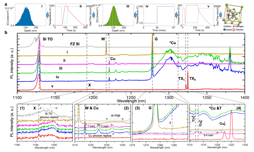
We examine a combination of different ion implantation and rapid thermal annealing processes to control and optimize the color center defect generation processes. Here, the T centers are generated by the following process adapted from earlier studies [54, 55]. A float-zone (FZ) grown, dilute boron-doped silicon substrate, whose resistivity is 1000 to 2000 with carbon and hydrogen impurity concentrations less than , is used. First, carbon ions are implanted into the silicon substrate at 7 degrees with 38 keV energy and a dose of . This implantation recipe produces an ion profile whose peak concentration is at 118.8 nm from the surface with 42.8 nm straggle based on SRIM-2013 simulations, with profile shown in Figure 1a-i [56].
The lattice damage from carbon implantation is repaired by rapid thermal annealing (RTA) at 1000 °C for 20 seconds in an argon environment with a flow rate of 3,000 sccm. The maximum temperature is achieved after a 28-second ramp-up, while the cooling is done passively under high argon flow (20,000 sccm). The temperature profile used is shown in Figure 1a-ii. This recipe is commonly used to introduce substitutional carbon centers in silicon to form G centers, which are examined as single-photon emitters [31, 30, 40]. In order to promote C-H groups needed to form the T centers, we subsequently implant hydrogen ions into the silicon substrate at 7 degrees with 9 keV energy and a dose of . As a result of this implantation, we obtain a hydrogen concentration profile illustrated in Figure 1a-iii with a peak concentration at 120.8 nm from the surface and with a straggle of 38 nm, matching the carbon concentration [56]. These samples are then cleaned using acetone and isopropyl alcohol and N2 blow-dried.
Afterward, the samples are treated in deionized water to promote hydrogen diffusion and bonding with carbon atoms. The treatment is done in a cleanroom setting under a fume hood, using a hot plate with a two-step process. The samples are treated in deionized water with a hot plate temperature of 115 °C for 30 minutes, subsequently with the hot plate increased to 180 °C and held for 37 minutes (Figure 1a-iv). Two-step treatment under fume hood is optimized to apply a controllable amount of thermal energy, with water surface temperature up to 95.5 °C. The treated samples are placed into the RTA chamber as the last step to promote the binding of C-H groups with substitutional carbon sites to form T centers. Inside the nitrogen environment, the samples are annealed at 420 °C for 3 minutes within a SiC susceptor, whose thermal properties may affect the actual temperature. The duration of annealing is varied to examine the changes. We also tested the outcomes when the samples were annealed without H2O treatment, which is important to protect the samples from oxygen contamination that contributes to the broadening of T center emissions.
Figure 1b shows the µPL spectrum taken between 1100 and 1400 nm at 5 K after each process step to examine the T center formation mechanism and its precursors compared to untreated Si substrate. As a benchmark of lattice damage in silicon, it can be observed that the silicon transverse-optical (TO) transition line around 1130 nm (bandgap) is completely destroyed under carbon implantation, which is recovered by RTA in step ii [57]. Owing to the low atomic mass, hydrogen implantation only shows a 10% decrease in Si TO line compared to step ii. Interestingly, the subsequent deionized water treatment also acts as an annealing process, which enhances the Si TO line damaged by hydrogen implantation. After the second RTA step, we observe a 30% decrease in Si TO line intensity, which might be due to the replacement of the Si sites with C-(C-H) complex that leads to the T centers formation [47]. We observe a similar trend in the Si phonon replica around 1195 nm. Superimposed on the phonon replica, after step v, we observe the presence of the weak X center line at 1191.7 nm. The origins of the X center are uncertain; initial propositions pointed out an interstitial nature with a possible tetrahedral or tetragonal symmetry, while the recent ab-initio studies on candidates such as I3-X or I4-A defects are inconclusive [58].
After carbon implantation at step i, prior to rapid annealing of the resulting lattice damage, we clearly observe the formation of W and G centers whose ZPL transitions are at 1217.48 nm and 1278.5 nm, respectively, with Gaussian full-width-at-half-maximum (FWHM) linewidths around 0.65 nm and 0.8 nm. The G center is a carbon-related defect, thought to be composed of two substitutional carbon sites connected by interstitial silicon [31, 30]. Here we observe the G line clearly without any annealing. The lifetime of the produced G center is also measured up to 6.67 ns at 7.5 K, which is slightly longer than the 5.9 ns reported previously for the ensembles but indicates the dominance of nonradiative processes[30, 35]. The W line has a phonon sideband up to 1250 nm, while the G line phonon sideband extends up to 1400 nm, including a local vibrational mode at 1381 nm [59]. Annealing at 1000 °C for 20 seconds, as shown in 1a-ii, however, leads to the disappearance of the G and W lines. This disappearance indicates the displacement of implantation-induced silicon interstitials into the lattice during thermal annealing. The W line is thought to be a cluster of interstitial silicon atoms in the lattice with a ZPL around 1218 nm [60, 61, 62, 58].
The W line is replaced in step ii by three phonon replicas at 1221.45, 1230.07, and 1238.64 nm with FWHM of 0.58, 1.2, and 1.65 nm, respectively, as shown in Figure 1b. These lines are about 7 meV apart from each other, indicating the energy of the involved phonons. The peak energies and separation are aligned with prior literature where it is identified as the Cu line, a complex of four Cu atoms [52, 63, 64, 50]. We observe a similar structure for the ∗Cu doublet peak around 1312.15 nm (Figure 1b-4 and Figure 2a), consisting of 0.56 meV split low (∗Cu) and high (∗Cu) energy lines at 1312.98 and 1312.20 nm respectively. Here, the superscript, m, indicates the number of phonons involved in the transition, hence denoting the phonon replicas, while the subscript, n, indicates the order of the transition in the excitonic energy ladder. We also observe alongside 6.4-meV phonon replicas at 1321.64 nm (called ∗Cu) and 1331.06 nm (called ∗Cu). These spectral peaks are formed after carbon implantation and RTA at 1000 °C, after step ii. We explain the fortuitous formation of Cu and ∗Cu peaks by possible Cu contamination during implantation and annealing steps, whose SIMS depth profile is given in Supplementary Materials as evidence. The Gaussian FWHM linewidth of the ∗Cu peak is around 0.66 nm, while the ∗Cu peak has a linewidth of 0.523 nm. These peaks disappear when deionized water treatment is applied. When we applied step v RTA process, without any water treatment, we were able to observe ∗Cu and ∗Cu peaks alongside the T center TX0 and TX1 lines, while the phonon replica at 1321.64 nm shows itself as a shoulder peak to TX1, denoted by ∗Cu.
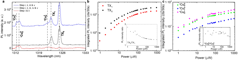
The RTA-only treatment is shown as the blue line dataset in Figure 2a. Our initial studies using secondary-ion mass spectroscopy verify the earlier studies that both the lines at 1221.45, 1230.07, and 1238.64 nm and the doublet denoted as ∗Cu and ∗Cu originate from residual Cu and/or Ag constituents during implantation. The 1221.45 nm line and the 7 meV-apart phonon replicas are identified as Cu-line, which is a precipitation of four Cu atoms [65, 64, 49, 50]. On the other hand, the 1312.15 nm doublet line and its phonon replica with 6.4 meV phonon energy at 1321.64 nm, belongs to a defect where a single Ag atom displaces one of the Cu atoms in the Cu-line, which is denoted as the ∗Cu center [52, 53, 49, 51, 50, 66]. We were able to replicate the formation of Cu and ∗Cu lines with deliberate Cu and Ag implantation into a Si wafer and RTA at 900 °C for 20 seconds, whose PL spectrum is provided in Supplementary Materials. We should also note that, as shown in Figure 2a, both the T centers and ∗Cu centers can be present simultaneously when water treatment is omitted, which suggests that ∗Cu center is also susceptible to hydrogenation under available thermal budget, either via implantation or deionized water treatment used for hydrogen diffusion.
The G center emission is recovered after hydrogen implantation. It results from the implanted-proton-induced interstitials and persists after the deionized H2O treatment [67]. However, it has a high-intensity phonon sideband from 1280 nm to 1400 nm, with the previously reported E-line evident at 1381 nm [59, 68], as observed in step i. Furthermore, after step v, a small peak is observed around 1285 nm, corresponding to the I-center, a variation of the T center perturbed by the presence of oxygen atoms [69]. The oxygen concentration is less than in the substrate.
As a result of the two-step treatment and RTA at 420 °C for 3 minutes, we obtained a clean TX0 zero-phonon line at 1325.1 nm with 0.63 nm linewidth and a TX1 line at 1322.65 nm with 0.79 nm linewidth. Figure 2a shows the TX0 and TX1 lines in the samples that are carbon and hydrogen implanted (after step iii), and RTA treated (after step v), and also the case where the samples are RTA treated only after step iii (without treatment). This indicates that, although deionized H2O treatment facilitates high-purity sample development, it is not required to induce T-center formation[55].
The integrated intensity of TX0 and TX1 emissions as a function of pump power is given in Figure 2b. The ZPL intensity area is saturated around 300 W. Presented in Figure 2b inset, at 1 W pump power, the ratio of ZPL intensity between TX0 and TX1 is around 2.725, which gradually decreases and reaches a minimum plateau point around 300 W where TX0 states saturate, while the optically injected carriers keep populating the TX1 states up to 500 W.
The same analysis is done for ∗Cu and ∗Cu peaks and the shoulder (∗Cu) peak we have discussed before. Similar to TX0 and TX1, the ∗Cu and ∗Cu intensities exhibit a saturation behavior at high pump power. Note that the broad ∗Cu line at the lower energy side of ∗Cu and ∗Cu lines follows the same trend as ∗Cu and ∗Cu, suggesting it can be attributed to a phonon replica. Unlike the T center, the intensity ratio between ∗Cu and ∗Cu begins around 2, staying constant up to 100 µW, and slowly decreases at higher power. Note that Cu center phonon replicas appear at the higher energy side of ∗Cu and ∗Cu lines (between 1221 nm and 1240 nm) (Figure 1b-2) while the T center spectrum (Figure 1b-4) is clean. As a result, a delayed decrease of the ∗Cu and ∗Cu intensity ratio can be due to the efficient carrier captured by the Cu centers.
II.1 Temperature dependent micro photoluminescence spectroscopy on T-center and defects
To investigate the nature of the observed ∗Cu doublet emission at 1312.15 nm, we performed a comparative study of the temperature-dependent µPL spectroscopy on the T center ZPL. Under low injection below PL intensity saturation, Figure 3a shows the temperature-dependent µPL spectra of the ∗Cu, ∗Cu and ∗Cu lines from 4.5 K to 30 K on an FZ silicon sample with carbon implantation and subsequent RTA process detailed in step i and ii of Figure 1a. A similar temperature-controlled measurement on the T center ZPL (TX0 and TX1) from 4.5 to 40 K is also performed on an FZ silicon sample with the fabrication process up to step v, and the µPL spectra are shown in the Supplementary Materials. Both defects show an isotropic dependency on the excitation polarization of the excitation as expected from an ensemble of doublets. In Figures 3b and 3c, it is shown that there is no preference of polarization between the doublets TX0-TX1 and ∗Cu-∗Cu, which may cause a population transfer between them.
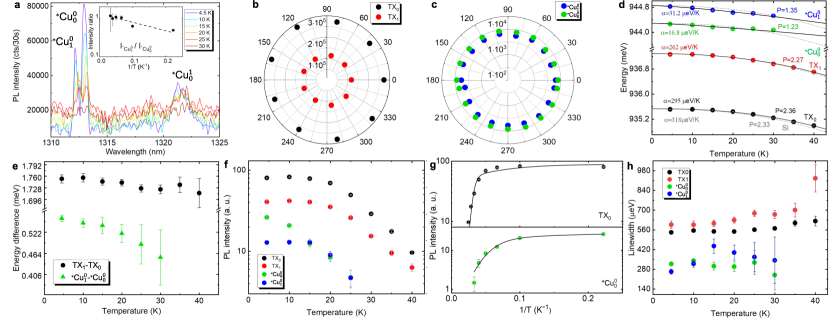
Figure 3d presents the temperature dependences of the , , and T-center ZPL transition energies extracted from Gaussian fits of their spectra. At cryogenic temperatures, the thermal-induced redshift of the semiconductor bandgap can be well expressed by the four-parameter model,
| (1) |
where denotes the slope in the limiting case of , is a dimensionless parameter related to the phonon dispersion coefficient , and approximately equals to the average phonon temperature [70]. For simple fitting purposes, Eq. (1) can be rewritten as a polynomial expression,
| (2) |
The transition energy of ∗Cu, ∗Cu, and T-centers are fitted using Eq. (2) and represented by the red curves. The dimensionless fitting parameter is equal to 1.25, 1.23, 2.27, and 2.36 for ∗Cu, ∗Cu, TX1, and TX0 transitions respectively. For comparison purposes, since the defect centers are in a sea of silicon atoms, we assume the average phonon temperature is the same and equals for silicon [70]. We can then extract the value of to be 31.2, 16.8, 262, and 295 µeV/K for ∗Cu, ∗Cu, TX1, and TX0 respectively. The silicon band gap variation with temperature is also plotted as grey dash lines along with the ∗Cu, ∗Cu, and T center by setting the parameters for silicon to be = 2.33, , and from [70]. For TX0 and TX1, their parameters are close to silicon values which indicates a smaller modification of the silicon matrix by the T center in the sample where steps i to v are performed. It suggests that the annealing and H2O treatment, which promotes the migration of carbon and hydrogen interstitials and leads to the T center formation, restore the lattice efficiently. In stark contrast, the red-shifting behavior of ∗Cu and ∗Cu transition energy exhibits a dramatic deviation from the silicon bandgap, resulting in a much smaller fitting parameter of and compared with the silicon and T center. This suggests that a significant distortion of the silicon matrix occurs during step i, where the injected carbon ions and displaced silicon atoms occupy the interstitial sites, creating vacancies in the implantation path.
The step ii promotes the impurity migration and results in the formation of 0.57 meV-split doublet luminescence centers. Notably, a much lower value of and result in a more significant phonon dispersion, and a smaller slope at suggests smaller zero-point renormalizations [71] by the dramatic modification of the electron-phonon interaction during its formation processes. This can also be in line with the observation of the vanishing W center ZPL and the appearance of phonon replicas. The significant phonon dispersion also leads to a higher dependence of doublet splitting of the ∗Cu and ∗Cu lines compared to the T center doublet. In Figure 3e, we observe that the energy difference between the ∗Cu and ∗Cu lines is reduced by at least 0.1 meV till about 30 K, before thermalization. On the other hand, the energy difference between TX0 and TX1 are somewhat constant across temperatures, owing to the smaller modification of the silicon matrix.
Figure 3f shows the integrated intensities of the ∗Cu, ∗Cu lines, and T centers ZPL with increasing temperatures. TX0 and TX1 start to thermalize around 20 K, while the ∗Cu line quenches much earlier. The intensity of the ∗Cu line exhibits a plateau up to 15 K. The measured meV spectroscopic splitting between the TX0 and TX1 lines at 4.5 K matches the reported value [72]. The known dissociation energy of the bound exciton of 22.5 meV [72] can be well-reproduced by fitting the TX0 intensity (black dots in Figure 3c) by a thermal partition function,
| (3) |
and setting meV as the excess energy of the excited state TX1 to TX0 and meV as the activation energy to the silicon band edge, which is shown as the black curve in the upper panel of Figure 3g. For the ∗Cu and ∗Cu lines, it is worth noting that their integrated intensity ratio (inset of Figure 3a) leads to a Boltzmann factor with a thermal activation energy of meV which agrees with the measured spectroscopic splitting of meV within our experimental error. It suggests that, like TX1 and TX0, the ∗Cu line can be associated with a transition from the higher excited state to the lower ∗Cu state of the same defect center. As shown in the lower panel of Figure 3g, Eq. (3) can be used to fit the ∗Cu intensity by setting to be the measured spectroscopic doublet splitting of 0.56 meV, with the resulting meV when the fit converges. This suggests a much smaller binding energy than the T center bound excitons and agrees with the much earlier intensity quenching of ∗Cu line even below 10 K. The total binding energy of the electron and hole associated with the bound exciton localized to this defect color center can be deduced to be 225.2 meV by subtracting transition energy of ∗Cu by the silicon bandgap at low temperature. Like the T center, probably suggests that such 0.57 meV-split doublet related luminescence center consists of one strongly localized and another loosely Coulombic bound particles, which is potentially another candidate for a spin-photon interface in the telecommunication band. Note that the PL intensity plateau of the ∗Cu line below 15 K is likely due to the thermal-induced carrier populating from the lower energy ∗Cu state to ∗Cu.
Figure 3h shows the temperature variation of FWHM linewidth. Both the lower energy states, TX0 and of the T-center and 0.56 meV-split doublet, exhibit a constant linewidth of about 542 eV and 318 eV, respectively, within our experimental error. However, for the higher energy states, TX1 linewidth stays constant at about 598 eV till around 20 K and increases to 927 eV at 40 K. The ∗Cu linewidth increases from 263 eV to 444 eV from 4.5 K to 15 K. It then gradually decreases to 343 eV at 30 K. The observed broadening with respect to the Fourier transform-limited linewidth of T center ( 1 neV) can result from: (1) fluctuating environmental charges which lead to pure exciton dephasing, or spectral diffusion, depending on the rate of energy Stark shifting; (2) ensemble emitting centers where individual ZPLs are shifted due to different local strains; (3) isotopic effects from natural silicon, in which the 29Si with non-zero nuclear spin cause resonance shift and magnetic field fluctuations; and (4) phonon-assisted broadening. However, for temperature variation of the linewidth, the phonon contribution is not significant for T = 30 K. We thus attribute the broadening of TX1 with temperature 30 K due to increasing charge fluctuations as a result of the thermal-induced electrons with increasing temperatures, considering the low pump regime (32 µW). The sudden increase at high temperature (40 K) can be due to increased phonon population and scattering. The minor variation of the TX0 linewidth compared to the TX1 linewidth can be due to its more localized exciton wavefunction, which also applies to the constant behavior of linewidth for the lower energy ∗Cu state compared to the higher energy doublet state. The dramatic increases of ∗Cu linewidth up to 30 K, in line with its thermalization above 30 K as shown in Figure 3f, can be attributed to increased charge fluctuations from the thermally-induced carriers, considering the small activation energy of 0.56 meV from ∗Cu to ∗Cu state. The subsequent decrease in the ∗Cu linewidth can be due to the charge stabilization of the fully occupied ∗Cu states at higher temperatures.
II.2 Photoluminescence dynamics of T-center and defects
The lifetime of the T center, a most likely candidate for next-generation spin-photon interface, was previously reported [28] but its radiative and non-radiative bound exciton dynamics are rarely studied. Thus, we performed the temperature-dependent time-resolved photoluminescence (TRPL) measurements on TX0 and TX1 color center transitions. We excite the sample with a pulse laser (600 nm, pulse width 5 ps) from an angle of about 45 degrees with the sample surface via a plano-convex singlet lens, creating a large excitation spot diameter of about 40 µm. We achieved sufficient counts for the TRPL histogram integration while refraining from saturating the T centers. PL is collected from the excitation spot via a 20 (NA = 0.4) microscope objective perpendicular to the sample surface and passes through a 0.5-meter monochromator to a near-infrared (NIR) photomultiplier tube (PMT) unit with 400 ps timing resolution attached to the exit port. The TRPL is then performed with the time-correlated single-photon counting (TCSPC) technique. The high-density 1200 grooves/mm grating achieves a spectral resolution of 0.04 nm so that only the ZPL of TX0 or TX1 feeds into the PMT, and the phonon sideband photons are rejected.
Figure 4a shows the resulting TRPL traces of TX0 transition with sample temperatures varying from 5 K to 40 K. The TX0 PL decay exhibits a prolonged tail and remains unchanged with increasing temperature until reaching 20 K, where it changes to a fast decay. Interestingly, as shown in the inset of Figure 4a, a slow rise of the TX0 PL intensity is visible at 5 and 10 K and gradually vanishes with increasing temperature. Such a slow rise component of the PL intensity and its variation with temperatures are neither observed in TX1 states and G centers (see Supplementary Materials), and nor observed in prior W [60], G [31, 30] and T centers [28, 54, 55]. We speculate that the carrier transition to TX0 from the higher excited states (TX2 to TX25) leads to a slow rise with the peak photoluminescence [28]. We phenomenologically explain this process using a simple two-level system coupled to the continuum of states, as shown in the inset of Figure 4b.
The measured PL decay of TX0 can be interpreted as the carrier relaxation from TX0 to a ground state with a lifetime (radiative and non-radiative) and a non-radiative carrier feeding from an effective higher excited state to TX0 with a characteristic time constant . Note that since the carrier transition from the silicon band edge is fast (tens of fs), [73, 74] it cannot be resolved in the measurement and thus absorbed into the initial carrier populations and . The following rate equations describe the carrier populations of and :
| (4) | |||
| (5) |
where and are the populations of the optically excited carriers in TX0 and higher excited states respectively. is the decay time of the TX0 state, and is the effective lifetime of higher excitation states. denotes the characteristic time constant of the non-radiative carrier feeding to TX0 states. denotes the total amount of available TX0 states that can be occupied.
As shown in Figure 4a, the TRPL trace of TX0 can be well-fitted by the model, and the extracted fitting parameters are shown in Figure 4b as a function of temperature. We extract a prolonged decay time of s at 5 K, which is 65% longer than the previously reported 0.94 s decay time [28]. and is much closer to expected lifetimes between 2 to 10s [75]. With increasing temperatures, decreases to ns at 40 K, where TX0 emission almost vanishes. Importantly, we observe the carrier transition lifetime of ns at 5 and 10 K, which contributes to the clear slow rising of TRPL traces and suddenly becomes slower with ns at 30 K. The observed 11 ns carrier transition and the resulting slow PL rising only observed for TX0 below 10 K can be caused by a much more localized nature of TX0 states. is three orders of magnitude faster than the decay of TX0, indicating a strong coupling between the localized TX0 and delocalized higher excited states.
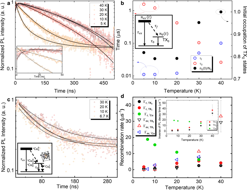
Considering that the pump power is fixed for TRPL measurement at all temperatures, the ratio of initial occupation of TX0 states to its total amount of available states, , show a sudden increase at 30 K, which indicates the start of thermal dissociation of TX0 bound exciton. Note that, due to the much slower temporary features of the PL, the timing resolution of the detector ( 400 ps) is negligible in the fit. We also perform the rate equation fitting by setting , where denotes the TX1 carrier population, but the simultaneous fitting of TX1and TX0 PL decay cannot be achieved. It agrees with the hypothesis that the non-radiative carrier transition is dominated by higher excited states, which also corresponds to our case of the above silicon bandgap pumping. The coupling between TX1 and TX0 states can be a much faster process that can only be investigated by resonantly pumping the TX1 state. Figure 4c shows the temperature-dependent TRPL of ∗Cu-∗Cu lines. Due to the small 0.56 meV-splitting and experimental limitations, both ∗Cu and ∗Cu lines are measured together with a TRPL window between 1309 and 1316 nm. With the presence of higher disturbance in the lattice (larger deviation of dashed model lines from the temperature-dependent fit of measured ∗Cudata from Si lattice) in Figure 3d), the ∗Cu-∗Cu decay occurs at a faster rate, with an excited state lifetime of 52.4 ns at 6.7 K. We observe an increase in the fitted lifetime at higher temperatures, to 71.2 ns at 30 K, due to the population transfer from ∗Cu to ∗Cu and higher excited states with slower decay rates. To further investigate the T center bound exciton recombination dynamics, we assume that both the radiative and non-radiative recombination channels contribute to the PL decay rate. The time-integrated PL intensity of TX0 and TX1 at temperature T is proportional to the quantum efficiency . With the radiative decay dominating the bound exciton recombination channel at T = 0 K, then can be written as:
| (6) |
where is extrapolated from Figure 3f and is the decay probability extracted from the rate equation fit of TX0 or the single exponential fit of TX1. Then, the radiative recombination rate can be obtained from equation (6). The resulting PL dynamical parameters of TX0 and TX1 as a function of temperature are plotted in Figure 4d. The inverse of the PL decay time of TX1 ( s) is nearly twice of TX0 at 5 K and shows a sudden increase after 30 K in-line with TX0 behavior. The extracted radiative and non-radiative bound exciton recombination rates of TX0 and TX1, with the experimental error bars, are shown as the inset. Compared with the non-radiative rate, the radiative rate of both TX0 (black circle) and TX1 (red circle) is relatively constant 1.5 and 3.6 respectively, corresponding to a Fourier-transform limited linewidth of 0.494 neV and 1.19 neV. The relatively temperature-independent rates (below 30 K) indicate potentially the suppression of thermally-induced fluctuation of the bound exciton wavefunction along any direction due to the three-dimensional quantum confinement[76]. A higher excited state (TX1) is anticipated to be more delocalized, indicated by a larger TX1 radiative rate. The slight increase in both TX0 and TX1 radiative rates with increasing temperature is due to the thermal-induced delocalization of the bound exciton wavefunctions. Above 30 K, the fast non-radiative decay starts to dominate both TX0 and TX1 recombination channels, which can be due to the thermal disassociation of bound excitons or the Shockley-Read-Hall (SRH) process induced by unwanted impurities or vacancies in natural Si, which results in the quenching of the T center PL intensity above 30 K. On the other hand, the radiative decay of combined ∗Cu emissions show an anomalous behavior, reducing with increased temperature from 18.76 at 6.7 K to 6.13 at 30 K, while the non-radiative recombination rate increase to 7.88 and becomes the dominant decay channel. This counterintuitive phenomenon here is attributed to the difference in decay rates and multiple phonon-assisted decay pathways (phonon replicas). We speculate that ∗Cu decay is faster than ∗Cu, which becomes dominant due to the population transfer at higher temperatures, as shown by the plateau in the ∗Cu observed in Figure 3f. After 30 K, the radiative decay of both ∗Cu and ∗Cu is thermalized by non-radiative and phonon-assisted decay through ∗Cu states, which is outside the spectral window of TRPL.
II.3 Magnetic-field induced broadening in the ensemble of and color centers
The T center bound exciton pairs with its ground state electron, which has a spin with an isotropic -factor of , to form a singlet with an unpaired hole spin with an anisotropic -factor in TX0 state [55]. Under a magnetic field, the unpaired hole spin leads to Zeeman splitting and diamagnetic shifts. The anisotropic hole spin leads to different -factors and diamagnetic shift coefficients based on the orientation of the defect in the lattice [41]. The total shift in the peak energy for spin-dependent lines can be identified as , where and are the -factors for electron and holes, is the Bohr magneton, is the diamagnetic shift due to higher-order Zeeman effect, and is the applied magnetic field [77]. The splitting enables a spin-photon interface that is essential for quantum memory applications. For this purpose, we examined the 0.56 meV-split doublet luminescence centers under a magnetic field to assess their potential.
For an ensemble of defects, each of the hole spins in a singlet state has a different -factor due to the different orientations in the lattice, leading to an additional inhomogeneous broadening of the PL spectrum under the magnetic field alongside the lifetime broadening, thermal broadening and the spectral diffusion between individual defect emissions. The resultant amplitude of the spin-polarized photoluminescence has a Voigt-like profile that accounts for these effects, described by the below [55, 77]:
| (7) |
Here, is detuning, & are Gaussian-broadened and homogeneous linewidths, and is the effective average Zeeman factor dependent on the hole -factor variations. This leads to an approximate Voigt linewidth [55].
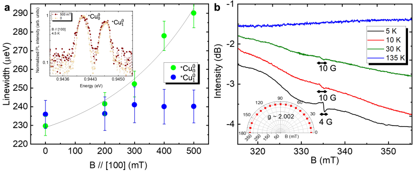
To assess the possibility of a spin-photon interface, we measure the magnetic-field-induced broadening of the 0.56 meV-split doublet line using non-resonant photoluminescence spectroscopy under an out-of-plane DC magnetic field ranging from 0 mT to 500 mT at 4.5 K. Instrumental limitations, and the broadening induced by the natural-Si substrate does not allow us to distinguish the spin-degeneracy-lifted transitions within the ensemble fully, but Figure 5a shows the magnetic-field-induced broadening of the ensemble ∗Cu color center transitions. The intrinsic Voigt linewidth at 4.5 K and 0 mT is measured as 229 eV for ∗Cu and measured as 235.9 eV for ∗Cu line. While there is not a significant broadening observed for the ∗Cu line, a sizable linewidth increase is observed for the first excited state ∗Cu, by 25% to 290 eV. This increase in the linewidth is much larger than the instrument resolution. Using Eq.7, we extract the effective Zeeman factor as 364 /T for the color center transition. Assuming that the novel doublet line is similar to T centers, we expect the formation of an unpaired hole-spin interacting with the ground-state electron within the first-excited transition of the ∗Cu-line. Further electron spin resonance analysis, which is given in Figure 5b, revealed that the ensembles of ∗Cu-∗Cu defects provide a lambda-type spin-photon interface, with a degenerate ground level split with an isotropic -factor of 2.002 and a Lorentzian broadening of 4 G, consistent with earlier observation for the isotropic triplet nature of the ∗Cu-peak [53]. The ESR resonance signal around 335 mT shows a Gaussian-like broadening of 10 G above 10 K and disappears completely above 30 K, which is consistent with the thermalization of the ∗Cu PL lines. This further strengthens that the magnetic-field induced broadening in Figure 5a is due to the spin degeneracy of ∗Cu line.
III Conclusion
In this study, we have examined the process steps leading to and T color centers’ formation. During the T center formation process, we observe that the well-known G and W centers are already present after low-dose carbon implantation. Subsequently, we observe interestingly that the G and W centers disappear after the annealing process at 1000 °C, only to be replaced by a doublet peak at 1312.15 nm ascribed as the and peaks, which are isoelectronic bound exciton peaks similar to T centers and originating from a Cu-Ag transition-metal color center. These optical transitions are present in the spectra of carbon implanted and annealed samples alongside the perturbed Cu-line phonon replicas. The Cu-line replicas between 1221.45 nm to 1238.64 nm and with 7 meV phonon energy are shown to confirm the predictions regarding the high electron-phonon coupling in W-centers. Furthermore, we have observed that the doublet optical transitions persist alongside TX0 and TX1 if the treatment is omitted and only RTA is applied to the sample. This doublet emission might lead to a novel spin-photon interface at O-band, and its magneto-optic properties will be examined further. We have examined and compared the TX0 and TX1 with and transitions and investigated their origins. The temperature-tuned PL measurement showed that the and peaks result from lower and higher excited states transitions, respectively, of the same color centers whose formation induces a higher perturbation to the silicon host, compared to the less perturbative T centers, in-line with the presence of the W-line phonon replicas. We further estimate a much smaller exciton binding energy associated with this novel defect, down to 3.35 meV.
Based on the abovementioned process, we examined the bound exciton dynamics of the generated ∗Cu and T color centers. With time-resolved PL measurements, we obtained radiative lifetimes of the ∗Cu transition at 52.4 4.8 ns, and for the T center at 1.56 0.13 , 65% longer than earlier studies [28]. Compared to previous recipes, the gradual introduction of H atoms by treatment may help to have a sample devoid of all defects other than T centers. Reducing possible non-radiative decoherence pathways, as evidenced by extended lifetime, is of utmost importance for high-fidelity network nodes, while cavity QED interactions can increase the coherent photonic qubit emission rates. We have confirmed our experimental results by fitting the rate equation modeling between TX0 and higher excited states, which leads to a slow carrier transition between TX1 and TX0, corresponding to the early-time slow-rising dynamics in our measured TRPL histograms. We further extracted the radiative and non-radiative recombination rates of the 3D confined T-center bound excitons.
The observed and improved T center lifetimes help to develop novel O-band quantum network nodes with high fidelity, involving cavity quantum electrodynamics of the spin-photon interface to control and route the emissions [29, 20]. The resolved ∗Cu doublet peak around 1312.15 nm offers a unique platform right at the zero-dispersion wavelengths in the O-band for qubit interactions. The determined excited-state radiative lifetimes magneto-optic and electron spin resonance measurements support the examinations of these silicon color centers towards solid-state quantum memories in scalable and metropolitan quantum networks.
IV Appendix - Experimental Setup
Power and temperature-dependent microphotoluminescence spectroscopy. A 532 nm solid-state continuous wave (CW) laser is used for the above-bandgap excitation with a continuous reflective neutral density (ND) filter for precise power control. A 925 nm dichroic mirror is used to reflect the incoming excitation laser to an objective (numerical aperture of 0.4) for focusing and PL collection. The samples are housed in a Lakeshore Janis ST-500 microscopy cryostat with a quartz window vertically set up. The collected PL is passed through the dichroic mirror and then a 905 nm long-pass filter to eliminate pump residual and directed into a Princeton Instruments 0.5-meter-long monochromator (SpectraPro 2500) with 600 g/mm grating. The magnetic-field-dependent measurements are done using room-temperature superconducting bore magnets with field intensities of 100, 200, 300, 400, and 500 mT. A liquid-nitrogen-cooled InGaAs camera is used to measure individual lines with a spectral resolution of about 100 pm.
Time-resolved microphotoluminescence spectroscopy.– The PL spectroscopy setup is modified to utilize a pulse laser at 600 nm selected from a supercontinuum source (NKT Photonics SuperK Extreme) at a 2 MHz repetition rate, which creates a 40 m spot on the sample with an angle of about 45 degrees for side pumping. The focal points of the side excitation path and the collecting Mitutoyo objective are aligned by co-propagation from both beam paths. The collected light is passed through the same spectrometer with 1200 g/mm grating (spectral resolution 40 pm) and directed to a photomultiplier tube (PMT). The RF-synchronized signal and PMT output are connected to a Swabian Instruments (TimeTagger 20) time-to-digital converter, achieving an overall timing resolution of 400 ps.
V Acknowledgements
The authors thank discussions with Joshua Pomeroy, Louis Bouchard, Madeline Taylor, and Kerry Kangdi Yu. The authors acknowledge support from the Army Research Office Multidisciplinary University Research Initiative (W911NF-21-2-0214), National Science Foundation under award numbers 2137984 (QuIC-TAQS) and 1936375 (QII-TAQS).
References
- Wei et al. [2022] S. Wei, B. Jing, X. Zhang, J. Liao, C. Yuan, B. Fan, C. Lyu, D. Zhou, Y. Wang, G. Deng, H. Song, D. Oblak, G. Guo, and Q. Zhou, “Towards Real‐World Quantum Networks: A Review,” Laser & Photonics Reviews 16, 2100219 (2022).
- Ritter et al. [2012] S. Ritter, C. Nölleke, C. Hahn, A. Reiserer, A. Neuzner, M. Uphoff, M. Mücke, E. Figueroa, J. Bochmann, and G. Rempe, “An elementary quantum network of single atoms in optical cavities,” Nature 484, 195–200 (2012), 1202.5955 .
- Reiserer and Rempe [2015] A. Reiserer and G. Rempe, “Cavity-based quantum networks with single atoms and optical photons,” Reviews of Modern Physics 87, 1379–1418 (2015).
- Wolfowicz et al. [2021] G. Wolfowicz, F. J. Heremans, C. P. Anderson, S. Kanai, H. Seo, A. Gali, G. Galli, and D. D. Awschalom, “Quantum guidelines for solid-state spin defects,” Nature Reviews Materials 6, 906–925 (2021).
- Hermans et al. [2022] S. L. N. Hermans, M. Pompili, H. K. C. Beukers, S. Baier, J. Borregaard, and R. Hanson, “Qubit teleportation between non-neighbouring nodes in a quantum network,” Nature 605, 663–668 (2022), 2110.11373 .
- Munro et al. [2022] W. J. Munro, N. L. Piparo, J. Dias, M. Hanks, and K. Nemoto, “Designing tomorrow’s quantum internet,” AVS Quantum Science 4, 020503 (2022).
- Reiserer [2022] A. Reiserer, “Cavity-enhanced quantum network nodes,” arXiv (2022), 10.48550/arxiv.2205.15380, 2205.15380 .
- Bhaskar et al. [2020] M. K. Bhaskar, R. Riedinger, B. Machielse, D. S. Levonian, C. T. Nguyen, E. N. Knall, H. Park, D. Englund, M. Lončar, D. D. Sukachev, and M. D. Lukin, “Experimental demonstration of memory-enhanced quantum communication,” Nature 580, 60–64 (2020), 1909.01323 .
- Qin, Miranowicz, and Nori [2023] W. Qin, A. Miranowicz, and F. Nori, “Proposal of ensemble qubits with two-atom decay,” arXiv (2023), 10.48550/arxiv.2302.06781, 2302.06781 .
- Coste et al. [2022] N. Coste, D. Fioretto, N. Belabas, S. C. Wein, P. Hilaire, R. Frantzeskakis, M. Gundin, B. Goes, N. Somaschi, M. Morassi, A. Lemaître, . I. Sagnes, A. Harouri, S. E. Economou, A. Auffeves, O. Krebs, L. Lanco, and P. Senellart, “High-rate entanglement between a semiconductor spin and indistinguishable photons,” (2022).
- Levonian et al. [2022] D. S. Levonian, R. Riedinger, B. Machielse, E. N. Knall, M. K. Bhaskar, C. M. Knaut, R. Bekenstein, H. Park, M. Lončar, and M. D. Lukin, “Optical Entanglement of Distinguishable Quantum Emitters,” Physical Review Letters 128, 213602 (2022), 2108.10928 .
- Stas et al. [2022] P.-J. Stas, Y. Q. Huan, B. Machielse, E. N. Knall, A. Suleymanzade, B. Pingault, M. Sutula, S. W. Ding, C. M. Knaut, D. R. Assumpcao, Y.-C. Wei, M. K. Bhaskar, R. Riedinger, D. D. Sukachev, H. Park, M. Lončar, D. S. Levonian, and M. D. Lukin, “Robust multi-qubit quantum network node with integrated error detection,” Science 378, 557–560 (2022), 2207.13128 .
- Lei et al. [2023] Y. Lei, F. K. Asadi, T. Zhong, A. Kuzmich, C. Simon, and M. Hosseini, “Quantum Optical Memory for Entanglement Distribution,” arXiv (2023), 10.48550/arxiv.2304.09397, 2304.09397 .
- Cozzolino et al. [2019] D. Cozzolino, B. D. Lio, D. Bacco, and L. K. Oxenløwe, “High‐Dimensional Quantum Communication: Benefits, Progress, and Future Challenges,” Advanced Quantum Technologies 2, 1900038 (2019), 1910.07220 .
- Erhard, Krenn, and Zeilinger [2020] M. Erhard, M. Krenn, and A. Zeilinger, “Advances in high-dimensional quantum entanglement,” Nature Reviews Physics 2, 365–381 (2020), 1911.10006 .
- Chang et al. [2021] K.-C. Chang, X. Cheng, M. C. Sarihan, A. K. Vinod, Y. S. Lee, T. Zhong, Y.-X. Gong, Z. Xie, J. H. Shapiro, F. N. C. Wong, and C. W. Wong, “648 Hilbert-space dimensionality in a biphoton frequency comb: entanglement of formation and Schmidt mode decomposition,” npj Quantum Information 7, 48 (2021), 2005.07759 .
- Yang et al. [2019] S. Yang, M. C. Sarihan, K.-C. Chang, C. W. Wong, and L. Dolecek, “Efficient Information Reconciliation for Energy-Time Entanglement Quantum Key Distribution,” 2019 53rd Asilomar Conference on Signals, Systems, and Computers 00, 1364–1368 (2019).
- Xiong et al. [2023a] Y. Xiong, C. Bourgois, N. Sheremetyeva, W. Chen, D. Dahliah, H. Song, S. M. Griffin, A. Sipahigil, and G. Hautier, “High-throughput identification of spin-photon interfaces in silicon,” arXiv (2023a), 2303.01594 .
- Berkman et al. [2023] I. R. Berkman, A. Lyasota, G. G. d. Boo, J. G. Bartholomew, S. Q. Lim, B. C. Johnson, J. C. McCallum, B.-B. Xu, S. Xie, N. V. Abrosimov, H.-J. Pohl, R. L. Ahlefeldt, M. J. Sellars, C. Yin, and S. Rogge, “Millisecond electron spin coherence time for erbium ions in silicon,” arXiv (2023), 10.48550/arxiv.2307.10021, 2307.10021 .
- Gritsch, Ulanowski, and Reiserer [2023] A. Gritsch, A. Ulanowski, and A. Reiserer, “Purcell enhancement of single-photon emitters in silicon,” Optica 10, 783 (2023), 2301.07753 .
- Ramanayaka et al. [2019] A. N. Ramanayaka, K. Tang, J. A. Hagmann, H.-S. Kim, D. S. Simons, C. A. Richter, and J. M. Pomeroy, “Use of quantum effects as potential qualifying metrics for “quantum grade silicon”,” AIP Advances 9, 125153 (2019).
- Tang et al. [2020] K. Tang, H. S. Kim, A. N. Ramanayaka, D. S. Simons, and J. M. Pomeroy, “Targeted enrichment of 28Si thin films for quantum computing,” Journal of Physics Communications 4, 035006 (2020).
- Dwyer et al. [2014] K. J. Dwyer, J. M. Pomeroy, D. S. Simons, K. L. Steffens, and J. W. Lau, “Enriching 28Si beyond 99.9998 % for semiconductor quantum computing,” Journal of Physics D: Applied Physics 47, 345105 (2014).
- Dwyer et al. [2017] K. J. Dwyer, H. S. Kim, D. S. Simons, and J. M. Pomeroy, “Temperature-dependent Si29 incorporation during deposition of highly enriched Si28 films,” Physical Review Materials 1, 064603 (2017).
- Tang et al. [2019] K. Tang, H. S. Kim, A. N. R. Ramanayaka, D. S. Simons, and J. M. Pomeroy, “A compact, ultra-high vacuum ion source for isotopically enriching and depositing 28Si thin films,” Review of Scientific Instruments 90, 083308 (2019).
- Saeedi et al. [2013] K. Saeedi, S. Simmons, J. Z. Salvail, P. Dluhy, H. Riemann, N. V. Abrosimov, P. Becker, H.-J. Pohl, J. J. L. Morton, and M. L. W. Thewalt, “Room-temperature quantum bit storage exceeding 39 minutes using ionized donors in silicon-28,” Science 342, 830–833 (2013), https://www.science.org/doi/pdf/10.1126/science.1239584 .
- Morse et al. [2017] K. J. Morse, R. J. S. Abraham, A. DeAbreu, C. Bowness, T. S. Richards, H. Riemann, N. V. Abrosimov, P. Becker, H.-J. Pohl, M. L. W. Thewalt, and S. Simmons, “A photonic platform for donor spin qubits in silicon,” Science Advances 3, e1700930 (2017).
- DeAbreu et al. [2019] A. DeAbreu, C. Bowness, R. J. Abraham, A. Medvedova, K. J. Morse, H. Riemann, N. V. Abrosimov, P. Becker, H.-J. Pohl, M. L. Thewalt, and S. Simmons, “Characterization of the Si:Se+ Spin-Photon Interface,” Physical Review Applied 11, 044036 (2019), 1809.10228 .
- Redjem et al. [2023] W. Redjem, Y. Zhiyenbayev, W. Qarony, V. Ivanov, C. Papapanos, W. Liu, K. Jhuria, Z. Y. A. Balushi, S. Dhuey, A. Schwartzberg, L. Z. Tan, T. Schenkel, and B. Kanté, “All-silicon quantum light source by embedding an atomic emissive center in a nanophotonic cavity,” Nature Communications 14, 3321 (2023), 2301.06654 .
- Beaufils et al. [2018] C. Beaufils, W. Redjem, E. Rousseau, V. Jacques, A. Y. Kuznetsov, C. Raynaud, C. Voisin, A. Benali, T. Herzig, S. Pezzagna, J. Meijer, M. Abbarchi, and G. Cassabois, “Optical properties of an ensemble of G-centers in silicon,” Physical Review B 97, 035303 (2018), 1708.05238 .
- Redjem et al. [2020] W. Redjem, A. Durand, T. Herzig, A. Benali, S. Pezzagna, J. Meijer, A. Y. Kuznetsov, H. S. Nguyen, S. Cueff, J.-M. Gerard, I. Robert-Philip, B. Gil, D. Caliste, P. Pochet, M. Abbarchi, V. Jacques, A. Dreau, and G. Cassabois, “Single artificial atoms in silicon emitting at telecom wavelengths,” Nature Electronics 3, 738–743 (2020), 2001.02136 .
- Durand et al. [2021] A. Durand, Y. Baron, W. Redjem, T. Herzig, A. Benali, S. Pezzagna, J. Meijer, A. Y. Kuznetsov, J.-M. Gerard, I. Robert-Philip, M. Abbarchi, V. Jacques, G. Cassabois, and A. Dreau, “Broad Diversity of Near-Infrared Single-Photon Emitters in Silicon,” Physical Review Letters 126, 083602 (2021), 2010.11068 .
- Lee et al. [2022] C.-W. Lee, M. Singh, A. C. Tamboli, and V. Stevanović, “Transition metal impurities in silicon: computational search for a semiconductor qubit,” npj Computational Materials 8, 172 (2022), 2105.05927 .
- Xiong et al. [2023b] Y. Xiong, C. Bourgois, N. Sheremetyeva, W. Chen, D. Dahliah, H. Song, S. M. Griffin, A. Sipahigil, and G. Hautier, “High-throughput identification of spin-photon interfaces in silicon,” arXiv (2023b), 2303.01594 .
- Liu et al. [2023] W. Liu, V. Ivanov, K. Jhuria, Q. Ji, A. Persaud, W. Redjem, J. Simoni, Y. Zhiyenbayev, B. Kante, J. G. Lopez, L. Z. Tan, and T. Schenkel, “Quantum Emitter Formation Dynamics and Probing of Radiation-Induced Atomic Disorder in Silicon,” Physical Review Applied 20, 014058 (2023).
- Baron et al. [2022a] Y. Baron, A. Durand, P. Udvarhelyi, T. Herzig, M. Khoury, S. Pezzagna, J. Meijer, I. Robert-Philip, M. Abbarchi, J.-M. Hartmann, V. Mazzocchi, J.-M. Gerard, A. Gali, V. Jacques, G. Cassabois, and A. Dreau, “Detection of Single W‑Centers in Silicon,” ACS Photonics 9, 2337–2345 (2022a), 2108.04283 .
- Hollenbach et al. [2022] M. Hollenbach, N. Klingner, N. S. Jagtap, L. Bischoff, C. Fowley, U. Kentsch, G. Hlawacek, A. Erbe, N. V. Abrosimov, M. Helm, Y. Berencén, and G. V. Astakhov, “Wafer-scale nanofabrication of telecom single-photon emitters in silicon,” Nature Communications 13, 7683 (2022), 2204.13173 .
- Saggio et al. [2023] V. Saggio, C. Errando-Herranz, S. Gyger, C. Panuski, M. Prabhu, L. D. Santis, I. Christen, D. Ornelas-Huerta, H. Raniwala, C. Gerlach, M. Colangelo, and D. Englund, “Cavity-enhanced single artificial atoms in silicon,” arXiv (2023), 10.48550/arxiv.2302.10230, 2302.10230 .
- Lefaucher et al. [2023] B. Lefaucher, J.-B. Jager, V. Calvo, A. Durand, Y. Baron, F. Cache, V. Jacques, I. Robert-Philip, G. Cassabois, T. Herzig, J. Meijer, S. Pezzagna, M. Khoury, M. Abbarchi, A. Dreau, and J.-M. Gerard, “Cavity-enhanced zero-phonon emission from an ensemble of G centers in a silicon-on-insulator microring,” Applied Physics Letters 122, 061109 (2023), 2210.05485 .
- Chartrand et al. [2018] C. Chartrand, L. Bergeron, K. J. Morse, H. Riemann, N. V. Abrosimov, P. Becker, H.-J. Pohl, S. Simmons, and M. L. W. Thewalt, “Highly enriched Si28 reveals remarkable optical linewidths and fine structure for well-known damage centers,” Physical Review B 98, 195201 (2018), 1807.10718 .
- Bergeron et al. [2020] L. Bergeron, C. Chartrand, A. T. K. Kurkjian, K. J. Morse, H. Riemann, N. V. Abrosimov, P. Becker, H. J. Pohl, M. L. W. Thewalt, and S. Simmons, “Silicon-Integrated Telecommunications Photon-Spin Interface,” PRX Quantum 1 (2020), 10.1103/prxquantum.1.020301, 2006.08793 .
- DeAbreu et al. [2023] A. DeAbreu, C. Bowness, A. Alizadeh, C. Chartrand, N. A. Brunelle, E. R. MacQuarrie, N. R. Lee-Hone, M. Ruether, M. Kazemi, A. T. K. Kurkjian, S. Roorda, N. V. Abrosimov, H.-J. Pohl, M. L. W. Thewalt, D. B. Higginbottom, and S. Simmons, “Waveguide-integrated silicon t centres,” Opt. Express 31, 15045–15057 (2023).
- Higginbottom et al. [2023] D. B. Higginbottom, F. K. Asadi, C. Chartrand, J.-W. Ji, L. Bergeron, M. L. Thewalt, C. Simon, and S. Simmons, “Memory and transduction prospects for silicon center devices,” PRX Quantum 4, 020308 (2023).
- Sarihan et al. [2022] M. C. Sarihan, J. Huang, W. Liu, J. H. Kang, B. Liang, and C. W. Wong, “Cryogenic O-band photoluminescence spectroscopy of T-centers in monolithic Si for mesoscopic cavity quantum electrodynamics,” Conference on Lasers and Electro-Optics , JTu3B.36 (2022).
- Fan et al. [2023] C. Fan, M. C. Sarihan, J. Huang, K. M. Azizur-Rahman, J. H. Kang, B. Liang, W. Liu, and C. W. Wong, “Cryogenic optical spectroscopy of color-centers in Si for quantum information processing,” CLEO 2023 , JTh2A.8 (2023).
- Huang et al. [2021] J. Huang, M. C. Sarihan, J. H. Kang, B. Liang, W. Liu, and C. W. Wong, “Cryogenic optical transitions of T centers in bulk Silicon and Silicon-on-insulator for cavi ty quantum electrodynamics,” Frontiers in Optics + Laser Science 2021 , JTu7A.2 (2021).
- Safonov et al. [1996] A. N. Safonov, E. C. Lightowlers, G. Davies, P. Leary, R. Jones, and S. Öberg, “Interstitial-Carbon Hydrogen Interaction in Silicon,” Physical Review Letters 77, 4812–4815 (1996).
- Song et al. [1990] L. Song, X. Zhan, B. Benson, and G. Watkins, “Bistable interstitial-carbon–substitutional-carbon pair in silicon,” Physical Review B 42, 5765 (1990).
- Steger et al. [2008] M. Steger, A. Yang, N. Stavrias, M. L. W. Thewalt, H. Riemann, N. V. Abrosimov, M. F. Churbanov, A. V. Gusev, A. D. Bulanov, I. D. Kovalev, A. K. Kaliteevskii, O. N. Godisov, P. Becker, and H.-J. Pohl, “Reduction of the Linewidths of Deep Luminescence Centers in Si28 Reveals Fingerprints of the Isotope Constituents,” Physical Review Letters 100, 177402 (2008).
- Steger et al. [2011] M. Steger, A. Yang, T. Sekiguchi, K. Saeedi, M. L. W. Thewalt, M. O. Henry, K. Johnston, H. Riemann, N. V. Abrosimov, M. F. Churbanov, A. V. Gusev, A. K. Kaliteevskii, O. N. Godisov, P. Becker, and H.-J. Pohl, “Photoluminescence of deep defects involving transition metals in Si: New insights from highly enriched 28Si,” Journal of Applied Physics 110, 081301 (2011).
- Vinh et al. [2004] N. Q. Vinh, J. Phillips, G. Davies, and T. Gregorkiewicz, “Time-resolved free-electron laser spectroscopy of a copper isoelectronic center in silicon,” Physical Review B 71, 085206 (2004).
- McGuigan et al. [1988] K. McGuigan, M. Henry, E. Lightowlers, A. Steele, and M. Thewalt, “A new photoluminescence band in silicon lightly doped with copper,” Solid State Communications 68, 7–11 (1988).
- McGuigan et al. [1989] K. McGuigan, M. Henry, M. Carmo, G. Davies, and E. Lightowlers, “A uniaxial stress study of a copper-related photoluminescence band in silicon,” Materials Science and Engineering: B 4, 269–272 (1989).
- Higginbottom et al. [2022] D. B. Higginbottom, A. T. K. Kurkjian, C. Chartrand, M. Kazemi, N. A. Brunelle, E. R. MacQuarrie, J. R. Klein, N. R. Lee-Hone, J. Stacho, M. Ruether, C. Bowness, L. Bergeron, A. DeAbreu, S. R. Harrigan, J. Kanaganayagam, D. W. Marsden, T. S. Richards, L. A. Stott, S. Roorda, K. J. Morse, M. L. W. Thewalt, and S. Simmons, “Optical observation of single spins in silicon,” Nature 607, 266–270 (2022).
- MacQuarrie et al. [2021] E. R. MacQuarrie, C. Chartrand, D. B. Higginbottom, K. J. Morse, V. A. Karasyuk, S. Roorda, and S. Simmons, “Generating T centres in photonic silicon-on-insulator material by ion implantation,” New Journal of Physics 23, 103008 (2021).
- Ziegler, Ziegler, and Biersack [2010] J. F. Ziegler, M. Ziegler, and J. Biersack, “SRIM – The stopping and range of ions in matter,” Nuclear Instruments and Methods in Physics Research Section B: Beam Interactions with Materials and Atoms 268, 1818–1823 (2010), 19th International Conference on Ion Beam Analysis.
- Henry et al. [1991] A. Henry, B. Monemar, J. L. Lindström, T. D. Bestwick, and G. S. Oehrlein, “Photoluminescence characterization of plasma exposed silicon surfaces,” Journal of Applied Physics 70, 5597–5603 (1991).
- Santos et al. [2016] I. Santos, M. Aboy, P. López, L. A. Marqués, and L. Pelaz, “Insights on the atomistic origin of X and W photoluminescence lines in c-Si from ab initio simulations,” Journal of Physics D: Applied Physics 49, 075109 (2016).
- Ivanov et al. [2022] V. Ivanov, J. Simoni, Y. Lee, W. Liu, K. Jhuria, W. Redjem, Y. Zhiyenbayev, C. Papapanos, W. Qarony, B. Kanté, A. Persaud, T. Schenkel, and L. Z. Tan, “Effect of localization on photoluminescence and zero-field splitting of silicon color centers,” Phys. Rev. B 106, 134107 (2022).
- Baron et al. [2022b] Y. Baron, A. Durand, P. Udvarhelyi, T. Herzig, M. Khoury, S. Pezzagna, J. Meijer, I. Robert-Philip, M. Abbarchi, J.-M. Hartmann, V. Mazzocchi, J.-M. Gerard, A. Gali, V. Jacques, G. Cassabois, and A. Dreau, “Detection of Single W‑Centers in Silicon,” ACS Photonics 9, 2337–2345 (2022b), 2108.04283 .
- Cherkova, Skuratov, and Volodin [2019] S. Cherkova, V. Skuratov, and V. Volodin, “Luminescence properties of FZ silicon irradiated with swift heavy ions,” Semiconductors 53, 1427–1430 (2019).
- Davies, Lightowlers, and Ciechanowska [1987] G. Davies, E. Lightowlers, and Z. E. Ciechanowska, “The 1018 meV (W or I1) vibronic band in silicon,” Journal of Physics C: Solid State Physics 20, 191 (1987).
- Estreicher and Carvalho [2012a] S. Estreicher and A. Carvalho, “The CuPL defect and the Cus1Cui3 complex,” Physica B: Condensed Matter 407, 2967–2969 (2012a).
- Fujimura and Shirai [2021] T. Fujimura and K. Shirai, “Revisiting the stable structure of the Cu4 complex in silicon,” Japanese Journal of Applied Physics 60, 021001 (2021), 1912.11586 .
- Estreicher and Carvalho [2012b] S. Estreicher and A. Carvalho, “The CuPL defect and the Cus1Cui3 complex,” Physica B: Condensed Matter 407, 2967–2969 (2012b).
- Vincent and Estreicher [2020] T. M. Vincent and S. K. Estreicher, “Ag and Ag–Cu interactions in Si,” Journal of Applied Physics 128, 155703 (2020).
- Schenkel et al. [2022] T. Schenkel, W. Redjem, A. Persaud, W. Liu, P. A. Seidl, A. J. Amsellem, B. Kanté, and Q. Ji, “Exploration of defect dynamics and color center qubit synthesis with pulsed ion beams,” Quantum Beam Science 6 (2022), 10.3390/qubs6010013.
- Thonke et al. [1981] K. Thonke, H. Klemisch, J. Weber, and R. Sauer, “New model of the irradiation-induced 0.97-eV (G) line in silicon: A C S- Si* complex,” Physical Review B 24, 5874 (1981).
- Gower et al. [1997] J. Gower, G. Davies, E. C. Lightowlers, and A. Safonov, “The I centre: A hydrogen related defect in silicon,” in Materials Science Forum, Vol. 258 (Trans Tech Publ, 1997) pp. 289–294.
- Pässler [1999] R. Pässler, “Parameter sets due to fittings of the temperature dependencies of fundamental bandgaps in semiconductors,” Physica Status Solidi (B) 216, 975–1007 (1999).
- Cardona and Thewalt [2005] M. Cardona and M. L. Thewalt, “Isotope effects on the optical spectra of semiconductors,” Reviews of Modern Physics 77, 1173 (2005).
- Irion et al. [1985] E. Irion, N. Burger, K. Thonke, and R. Sauer, “The defect luminescence spectrum at 0.9351 eV in carbon-doped heat-treated or irradiated silicon,” Journal of Physics C: Solid State Physics 18, 5069 (1985).
- Sjodin, Petek, and Dai [1998] T. Sjodin, H. Petek, and H.-L. Dai, “Ultrafast carrier dynamics in silicon: A two-color transient reflection grating study on a (111) surface,” Physical Review Letters 81, 5664 (1998).
- Wörle et al. [2021] M. Wörle, A. W. Holleitner, R. Kienberger, and H. Iglev, “Ultrafast hot-carrier relaxation in silicon monitored by phase-resolved transient absorption spectroscopy,” Physical Review B 104, L041201 (2021).
- Dhaliah et al. [2022] D. Dhaliah, Y. Xiong, A. Sipahigil, S. M. Griffin, and G. Hautier, “First-principles study of the T center in silicon,” Physical Review Materials 6, L053201 (2022).
- Rosales et al. [2013] D. Rosales, T. Bretagnon, B. Gil, A. Kahouli, J. Brault, B. Damilano, J. Massies, M. V. Durnev, and A. V. Kavokin, “Excitons in nitride heterostructures: From zero- to one-dimensional behavior,” Physical Review B 88, 125437 (2013).
- McGuyer et al. [2015] B. H. McGuyer, M. McDonald, G. Z. Iwata, M. G. Tarallo, W. Skomorowski, R. Moszynski, and T. Zelevinsky, “Precise study of asymptotic physics with subradiant ultracold molecules,” Nature Physics 11, 32–36 (2015).