Observation of Dirac like surface state bands on the top surface of BiSe
Abstract
Two quintuple layers (QLs) of strong topological insulator (TI) Bi2Se3 are coupled by a Bi bilayer in BiSe crystal. We investigated its electronic structure using angle resolved photoelectron spectroscopy (ARPES) to study its topological nature. Dirac like linearly dispersive surface state bands (SSBs) are observed on the (001) surface of BiSe and Sb doped (8%) BiSe, similar to Bi2Se3. Moreover, the lower part of the SSBs buries deep in the bulk valence band (BVB). Overlap region between the SSBs and BVB is large in Sb doped system and the SSBs deviate from the Dirac like linear dispersion in this region. These results highlight the role of interlayer coupling between the Bi bilayer and the Bi2Se3 QLs. Furthermore, we observed a large intensity imbalance I(k||) I(-k||) in the SSBs located at the positive and negative k|| directions. This asymmetry pattern I(k|| ) I(-k||) gradually reverses to I(k||) I(-k||) as the excitation energy scans from low (14eV) to high (34eV) value. However, we did not observe signal of surface magnetization resulting from the intensity imbalance in SSBs due to hole-generated uncompensated spin accumulation in the photoexcitation process. The main reason for this could be the faster relaxation process for photo-hole due to the presence of the Bi bilayer between the adjacent Bi2Se3 QLs. The observed photon energy dependent intensity variation could be a signature of the mixing between the spin and the orbit texture of the SSBs.
pacs:
74.25.Jb, 73.20.At, 74.70.DdI Introduction
The discovery of spin polarized non-trivial gapless topological surface states in bulk insulating materials has been a major breakthrough in the field of condensed matter physicsrev ; rev1 . Various exotic states of these compounds, which are widely known as topological insulators (TIs), are being investigated and understood using both experimental and theoretical tools. Lots of research work is also being devoted to explore the technologically important properties of these materials such as the effect of proximity of TIs with superconductorsab , correlated and magnetic materialshong , the spin helical SSBs of TIs to build up some novel devices, especially in the area of spintronicsab1 and quantum computingmaj ; maj1 .
Various compounds of the Bi chalcogenides family, like Bi2Se33dtopo ; dirac , Bi2Te3wrap2 and Bi1-xSbxSe1-yTeybsts ; bsts1 ; sato ; hor exhibit strong TI characteristics. BiSe is one of the member of this family which shows a rhombhohedral crystal structurebise ; bise1 . This structure consists a Bi2 bilayer between two Bi2Se3 quintuple layers (QLs). Bi bilayers has been recongnised as a quantum spin hall insulators, whereas Bi2Se3 is well known strong TI. Therefore, this combined structure of Bi bilayer and Bi2Se3 QL i. e. BiSe is interesting to study topological properties. In our previous study we found a clear weak-anti-localization (WAL) cusp in magneto-resistance measurements in the low filed region. This indicates that BiSe hosts topologically protected surface statesbise . The WAL coefficient defined in Hikami-Larkin-Nagaoka (HLN) equation is 0.42 which is close to a value of 0.5. This is the value expected for a single coherent channel having a Berry phasehnn . DFT predicts two Dirac cones at its side surfaces (100). On the other hand, SSBs at top surface (001) depends on its stoichiometry. It is Rashba type SSBs if the top surface contains Bi bilayer while no Dirac like SSBs are found at Se terminationbise . However, it is very hard to directly observe Dirac like SSBs by probing the side surfaces of BiSe using ARPES due to non-cleavability of its side surfaces.
In this paper we present our ARPES results on single crystals of BiSe and a Sb doped version of it with formula Bi0.92Sb0.08Se. Dirac like linearly dispersing SSBs are observed on the top surface (001) of BiSe. Furthermore, the Dirac point (DP) is placed deep in the bulk valence band (BVB). Sb doping not only increases this overlap between the SSBs and BVB but affects the linearity of the SSBs dispersion as well. This behavior is quite different from those shown by the known TIs of the Bi family Bi2Se3. The difference could be due to the interlayer coupling between the Bi bilayer and the Bi2Se3 QL. Interestingly, we noticed an appreciable amount of intensity imbalance in the SSBs located at the positive and negative k|| directions and also it is sensitive to the variation in the excitation energy. This possibly indicates a mixing between the spin and the orbital texture in the SSBs. These results also highlight the role of the Bi bilayer existing between the adjacent Bi2Se3 QLs in this material which enhances the relaxation process for the photo-hole generated at the SSBs.
II Experimental Details
High quality BiSe single crystals used in this study were synthesized by modified Bridgman method. Crystallinity of the samples was confirmed by using X-ray diffraction measurements and the elemental composition by energy dispersive X-ray (EDX) analysis. Details of other measurements of the physical properties can be found elsewherebise . Photoemission measurements were performed at the BaDElPh beamlineluca of the Elettra synchrotron center, (Trieste, Italy), equipped with a SPECS Phoibos 150 hemispherical analyser. The energy and angular resolutions of the ARPES measurements were set to 20meV and 0.3∘, respectively. The measurements were carried out at room temperature under ultra high vacuum conditions with a base pressure of 5.0 10-11mbar. The single crystalline samples were cleaved in-situ and their orientation were determined by using low energy electron diffraction (LEED).
III Results and Discussion
Fig.1 shows the results of our ARPES measurements on the BiSe crystal by using photons of a wide energy range (14eV to 34eV) performed with the aim to map its three dimensional electronic structure. Fig.1(a)-(e) depict the high resolution ARPES images of a few selected photon energies (18eV to 32eV). Two linearly dispersing bands could clearly be seen and between these two bands an intensity patch of parabolic shape is also visible close to the Fermi level (Ef). Some intensity is also visible at the higher binding energy (BE) region BE 0.7eV which could correspond to the bulk valence band (BVB). While the linearly dispersive bands remain intact as the photon energy varies, a relative change can be noticed in the parabolic intensity pattern near the Ef.
To further analyse this point, we constructed constant energy contours (CEC) by using the momentum distribution curves (MDC) at BE = 0.0eV (Fig.1(f)) and 0.1eV (Fig.1(g)) from the ARPES images corresponding to photon energy of 14eV to 34eV, respectively. Here in Fig.1(g), the intensity pattern shows a constant (white dotted lines are drawn as guide for the eye) structure at k|| 0.23Å-1. This confirms that these external bands belong to the surface since they are independent of the kz value associated to photon energies 14eV to 34eV. Furthermore, the variation in the intensity profile between the two linear bands indicates the bulk origin of the parabolic band near Ef. These bulk and surface originated states are labeled as SSB and BVB/bulk conduction band (BCB) in the ARPES image of 25eV.
In addition, we found that the SSBs extend quite deep into the BVB. This is quite anomalous compared to the known TIs of the Bi chalcogenide family, such as Bi2Se33dtopo ; dirac ; bsts1 and BiSbTe1.25Se1.75bsts , where the SSBs remains well separated from the BVB and the Dirac point appears close to the top of the BVB. We have further discussed this point in the following paragraph where we compared the ARPES data from BiSe and Sb doped BiSe.
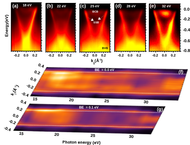
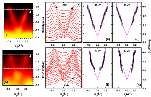
Fig.2(a) and (b) show ARPES images of the -M oriented sample of BiSe and Bi0.92Sb0.08Se, respectively, measured at an excitation energy of 30eV. In case of BiSe, the SSBs can be distinguished clearly, and in the higher BE region overlap strongly with the BVB states positioned at BE 0.7eV. Instead, in Bi0.92Sb0.08Se (Fig.2(b)) BCB states are absent at Ef and a measurable shift towards Ef is observed in the deeper lying BVB states in comparison to those of BiSe. This shifted BVB covers a large portion of the SSBs and they are resolved only in the vicinity of Ef. This is also clear from the MDC profiles stacked in Fig.2(c) and (d) extracted from Fig.2(a) and (b) for energy ranging from -0.47eV to -0.08eV and -0.39eV to 0.0eV, respectively. In BiSe the MDC profile at BE close to Ef (Fig.2(c)) shows two well resolved peaks corresponding to the SSBs. As the BE increases the two peaks start coming closer to each other and it becomes too difficult to resolve them beyond BE 0.53eV. On the other hand, in the case of Bi0.92Sb0.08Se (Fig.2(d)), the MDC peaks representing the SSBs are less pronounced. Here also, the two SSB peaks become a single peak at higher BE similarly as for BiSe. However, a clear hump structure can be noticed at k|| 0.25Å-1 in the MDC profile at higher BE which indicates the BVB. In Bi0.92Sb0.08Se the BVB feature overlaps with the SSBs dispersion, as inferred from the ARPES images and the MDC plots.
Furthermore, we extracted the SSBs dispersion from these ARPES images of BiSe and Bi0.92Sb0.08Se by tracking the peak position of the SSB feature in the MDC spectra at different BE and results are shown in Fig.2(e) and (f) respectively. These experimental data are also fitted to the following calculated band dispersion (magenta line)fu ; lu
| (1) | ||||
where E± corresponds to the energy of upper and lower bands, Ed is Dirac energy, m∗ denotes the effective mass, and indicates the azimuthal angle of momentum with respect to the x-axis (-K direction). is a parameter for the hexagonal warping. is the Dirac velocity which is modified to after including a second order correction parameter () to the Dirac velocity in the k p Hamiltonian. BiSe data show a reasonably good fit to the calculated bands whereas in the case of the Sb doped compound the fitted band slightly deviates from the experimental SSBs especially in the higher BE region. In order to confirm this difference, the SSB dispersions of BiSe (Fig.2(g)) and Bi0.92Sb0.08Se (Fig.2(h)) are compared also at a different photon energy. For BiSe the calculated SSBs fit well with the experimental data at 25eV photon energy, like the previous case of 30eV photon energy (Fig.2(e)). However, in Bi0.92Sb0.08Se at excitation energy 24eV some discrepancy could be seen again at the higher BE region where the contribution from the BVB starts to be also significant (see also Fig.S2 of supp. info.).
Fitting parameters are listed in Table.1. We found that the value of is 2.2eV.Å for BiSe which is smaller compared to the value found in other compounds of the Bi chalcogenide family such as Bi2Se3 ( 3.2eV.Å)dirac or BiSbTe1.25Se1.75bsts ( 3.0eV.Å). The table also shows that with Sb doping the m∗ of the SSBs reduce by 40% while increases by 19% . This result is different from the case of Bi2Se3 thin films where it has been found that Sb acts as an electron acceptor for the electronic charge segregated at the surface and consequently just pulls the whole electronic structure towards the Ef without affecting the appreciablythinfilm . This difference could be due to the different interlayer coupling in BiSe; between the Bi bilayer and its adjacent Bi2Se3 QLs. The role of Bi bilayer has been thoroughly investigated in previous DFT studies and were pointed out the possibility of various SSBs in (Bi2)n(Bi2Se3)mgov ; bise . In a slab structure (Bi2Se3)5(Bi2)2, where a Bi bilayer is situated on the top of 5 Bi2Se3 QLs, two Dirac like SSBs originating from the top and bottom QLs are present at higher BE compared to original slab of 5 Bi2Se3 QLs. It occurs due to two reasons. One is the Bi bilayer structural relaxation to the Bi2Se3 slab and second is a charge transfer from the Bi bilayer to the adjacent Bi2Se3 QL. This charge transfer also creates an internal electric field and that produces a Rashba splitting in the Bi bilayer SSBs which is found at Ef. In the other case, where the Bi bilayer resides between the Bi2Se3 QLs ( (Bi2Se3)3(Bi2)2(Bi2Se3)2 ) Dirac like SSBs also exist and they are localized at the topmost and bottommost QL. They also resides at higher BE compared to the bare slab of 5 Bi2Se3 QLs. Thus, in both the situations the SSBs of Bi2Se3 QLs are affected in the presence of Bi bilayer. This prediction is consistent to current experimental results on BiSe where we found that the DP at BE 0.66eV resides at higher BE in comparison to Bi2Se3 ( 0.3eV)dirac . Similarly, the SSBs cut the Ef at larger k|| ( kf 0.23Å-1 ) than in the case of Bi2Se3 ( 0.08Å-1 ).
Apart from the different DP and kf value of the SSBs in BiSe compared to Bi2Se3, the emergence of the BVB states adjacent to the SSBs is also quite peculiar as it influences the evolution of SSBs in doped TIs. For example, in case of TlBi(S1-xSex)2 it has been reported that while the BVB remains almost intact only the massless Dirac SSBs become gradually massive as a function of sulphur dopingnewref . Therefore, increment in the overlap region between the BVB and SSBs due to a large movement in the BVB towards Ef shows that the bulk electronic structure of BiSe is highly sensitive to the Sb doping. This could again be the result of a change in the coupling strength between the Bi bilayer and the Bi2Se3 QL due to the dopant. Nevertheless, the existence of SSBs in Bi0.92Sb0.08Se shows that the SSBs are topologically protected against this doping. Of course, there are some deviations from the linearity in the SSBs dispersion in specific regions where the SSB overlaps with the BVB. This reshaping of the SSBs has recently also been found in Bi2Se3, where a non-magnetic impurity produces a kink-like feature in the upper part of the SSBsreson .
| BiSe | ||||
| h(eV) | m⋆/m | (eV.Å) | (eV.Å3) | Ed(eV) |
| 30 | 2.1 | 2.2 | 2.0 | 0.66 |
| 25 | 1.9 | 2.0 | 2.0 | 0.64 |
| Bi0.92Sb0.08Se | ||||
| 30 | 1.2 | 2.5 | 2.0 | 0.61 |
| 24 | 1.2 | 2.6 | 2.0 | 0.62 |
Fig.3(a) shows the MDC at Ef of the BiSe sample taken at the azimuthal angles 0∘ (black, -M direction), 5∘ (red) and 10∘ (blue) at photon energy 18eV. These spectra depict the presence of four peaks in which the outer two (green dotted line) belong to the SSBs and the inner two peaks (magenta dotted line) correspond to the BCB. It can be noted from this plot that the intensity of the SSB peak at positive k|| (P2) is larger compared to the peak at negative k|| (P1). However, in the azimuthal data collected at 30eV (Fig.3(b)) we found that the intensity of the SSB peak P1 increases and becomes comparable to that of the SSB peak P2. For further investigation, the intensity ratio Idiff = (I(P1) - I(P2)) / (I(P1) + I(P2)) from the MDC peaks P1 and P2 is calculated at various photon energies. Results are presented in Fig.3(c) where red, blue, green and black data correspond to the intensity ratio obtained from the MDC profiles at BE = 0.0, 0.10, 0.20 and 0.50eV, respectively. The intensity ratio at BE = 0.0eV is negative at lower photon energies (16eV) and it gradually increases with the excitation energy, and at higher energies (32eV) this ratio becomes positive. The intensity ratio at BE = 0.10 and 0.20eV remains almost same at the lower photon energy region (16 to 20eV) whereas it decreases at the higher photon energy side (30 to 34eV). To illustrate this point, MDC profiles (at BE = 0.0, 0.10 and 0.20eV) extracted from the ARPES images at lower and higher photon energies of 18eV (black) and 33eV (red) are shown in the Fig.3(d), (e) and (f). It is evident in these plots that the SSB peak at negative k|| direction (P1) has less intensity compared to its counterpart at the positive k|| direction (P2) at low photon energy and vice versa. On the other side, at higher BE position BE = 0.50eV the intensity ratio does not show any noticeable change as the photon energy varies from 14eV to 34eV. The intensity imbalance remains sensitive to the photon energy variation in Sb doped case as well (see Fig.S3 of supp. info.)
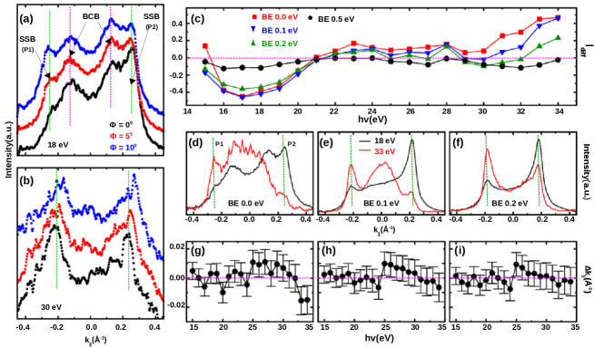
It may appear that this photon energy dependence of the intensity imbalance in the kx - ky plane could probably be explained in terms of transition matrix elements involved in the photoemission process. In this process generally, final states are approximated to plane waves and thereby matrix elements mainly depends on the initial stateshuf ; luca1 . In that case, we can expect the intensity ratio to remain the same in Fig.3(c) for all the different BEs because these BEs correspond to various parts of the same SSBs. Since this is not the case, the intensity imbalance must be linked to some other factors. The ARPES spectral weight along different k directions can reveal the nature of the spin texture of the SSBs in TIs. Previously, it has been reported by Jozwiak et al. that in case of Bi2Se3 the electrons in the SSBs at positive and negative k|| have the character of up and down spin, respectively and this spin helicity interchanges gradually with change in the incident light polarization from s to psoc . This change is reflected in the spin-resolved photoemission intensity of the SSBs which varies with the polarization. Furthermore, it has been found that spin polarization of the SSBs in Bi2Se3 not only coupled to crystal momentum but also to the orbital component due to strong spin-orbit interactionsoc3 . From DFT calculations Zhu et al. have revealed the wave function of topological surface states () is composed of out-of-plane pz orbital as well as in-plane px,y orbitals. And the contribution of different orbitals in the varies at different layers within the topmost 2 QLs in which the is confined. Spin polarization of the mainly entangles with the in-plane orbital components and thereby a layer dependent spin-orbital texture is formed. Due to this layer dependent , photoemission matrix element results asymmetric intensity distribution of SSBs in CEC contour (kx,ky) at BE 0.1 eV above the DP. This intensity pattern changes to a different pattern as BE varies 0.2 eV above the DPsoc1 . Therefore, the asymmetric intensity pattern I(k||) I(-k||) we observed in the SSBs of BiSe could be related to layer dependent spin-orbital texture. With this understanding it is difficult to reconcile the photon energy dependency of the Idiff (Fig.3(c)) because the orbital character of SSBs is independent to kz value associated to different photon energies. However, we can understand this Idiff variation in terms of matrix element effects if the final states are not simple plane waves but have a complex structure, like p or d type states as already pointed out by Vidal et al. in circular dichroism ARPES study of Bi2Se3soc2 . In this scenario, matrix element which connects the layer dependent to different possible final states can lead to photon energy dependent change in the Idiff.
Furthermore, in a recent study on pristine and magnetically doped TI Bi2Te2Se, Shikin et al.luca1 also found an asymmetric intensity distribution on the left and right branch of the SSBs and its dependency on the photon energy. They proposed that this intensity imbalance could develop some surface magnetism under the influence of synchrotron radiation due to hole-generated uncompensated spin accumulation. Consequences of the in-plane and out-of-plane magnetic moments are a shifted position of the DP from k|| = 0.0Å-1 and a gap opening at the DP position. Both of these signatures are observed prominently in the vanadium doped TI Bi1.37V0.03Sb0.6Te2Se.
In our case, we also observed a very slight asymmetry in the position of the SSBs at positive and negative k|| direction. To study this point, mid point k|| value (k0) between the SSB peaks P1 and P2 of MDC profile at BE = 0.50eV is chosen as reference with the k|| = 0.0Å-1 because intensity imbalance is almost absent in this MDC spectra (Fig.3(c)). We estimated the shift (k||) in the k0 value from the k|| = 0.0Å-1 for the MDC profile at BE = 0.0, 0.10 and 0.20eV for various excitation energies and results are depicted in Fig.3(g), (h) and (i), respectively. Unlike the intensity ratio, the k|| does not exhibit any significant variation (within the error bar limit) with respect to the photon energy. In this analysis, the peak positions of P1 and P2 are obtained directly from the MDC spectra to determine the k0 because asymmetry associated to the MDC spectra hinders a reasonable fitting to estimate the peak positions. To calculate the error in the k|| measurements we used the formulahuf k|| = 0.512cos() [Å-1], where represents the photoelectron acceptance angle with respect to the sample normal along the analyser slit. Moreover, the change in the k0 (Fig.3(g)) is not large enough to quantify the radiation induced magnetization. Reason for this could be the absence of magnetic doping and large thermal fluctuations at room temperature. On the other hand, the shift in k0 is further reduced at higher BE (Fig.3(h) and (i)) despite the significant intensity imbalance at these BE (Fig.3(c)). Therefore, it can also be possible that the presence of the Bi bilayer between the adjacent Bi2Se3 QLs provides a faster relaxation route to the holes generated at the SSBs and thereby the accumulation of uncompensated spin on the SSBs is suppressed.
IV Conclusion
Our ARPES results on BiSe show the presence of Dirac like linearly dispersive SSBs around the point at its top surface (001). The SSBs are located deep in the BVB and with a small (8%) Sb doping their overlap with the BVB increases significantly. The SSBs deviate from the Dirac like linear dispersion in this overlap region. This evolution of the SSBs with doping is quite different from those shown by other known TIs of the Bi chalcogenide family, like for instance Bi2Se3, Bi2Te3 and BiSbTe1.25Se1.75. The reason for this difference could be linked to the interlayer coupling between the Bi bilayer and Bi2Se3 QL. Another observation of this study is the asymmetry in the spectral weight of the SSBs between the positive and negative k|| directions. This asymmetry gradually switches to the opposite direction as the photon energy varies. This photon energy dependent intensity variation could be a signature of the mixing between the spin and the orbit texture of the SSBs. We also observed that the intensity imbalance in the SSBs leads an almost zero shift in the DP position in BiSe due to an accumulation of uncompensated spin. While the effect is clearly reported for Bi2Te2Seluca1 , in BiSe we find a reduced magnitude of it that can be explained with the presence of Bi bilayer between the adjacent Bi2Se3 QLs of this material. These results have significance in understanding the spin-orbital texture of the SSBs in BiSe. These are also helpful for further investigations on weak TIs. Because theory predicts weak TI can form by joining strong TIs via week coupling, like situation in BiSe where a Bi bilayer couples two QLs of strong TI Bi2Se3.
Acknowledgements: H.L. is supported in part at Israel Institute of Technology, Technion by a PBC fellowship of the Israel Council for Higher Education. K.M., P.S.A.K. and B.R.S. acknowledge the support by Department of Science and Tech- nology, Government of India for accessing the Elettra Syn- chrotron.
References
- (1) M. Z. Hasan and C. L. Kane Rev. Mod. Phys. 82 (2010) 3045.
- (2) X. L. Qi and S. C. Zhang Rev. Mod. Phys. 83 (2011) 1057.
- (3) A. Banerjee, A. Sundaresh, R. Ganesan and P.S.A. Kumar ACS Nano 12, (2018), 12665.
- (4) P. Zhang, Z. Wang, X. Wu, K. Yaji, Y. Ishida, Y. Kohama, G. Dai, Y. Sun, C. Bareille, K. Kuroda, T. Kondo, K. Okazaki, K. Kindo, X. Wang, C. Jin, J. Hu, R. Thomale, K. Sumida, S. Wu, K. Miyamoto, T. Okuda, H. Ding, G. D. Gu, T. Tamegai, T. Kawakami, M. Sato and S. Shin Nat. Phy. 15 (2019) 41.
- (5) A. Banerjee, A. Sundaresh, K. Majhi, R. Ganesan, and P.S.A. Kumar App. Phy. Lett. 109 (2016) 232408.
- (6) L. Fu and C.L. Kane Phy. Rev. Lett. 100 (2008) 096407.
- (7) D. Hsieh, Y. Xia, L. Wray, D. Qian, A. Pal, J.H. Dil, J. Osterwalder, F. Meier, G. Bihlmayer, C.L. Kane, Y.S. Hor, R.J. Cava and M.Z. Hasan Science 323 (2009) 919.
- (8) C.L. Kane and E.J. Mele Phys Rev Lett., 95, (2005), 146802.
- (9) L. Fu and C.L. Kane Phys. Rev. B, 76, (2007), 045302.
- (10) Z. Ringel, Y.E. Kraus, and A. Stern Phys. Rev. B, 86, (2012), 045102.
- (11) H. Zhang, C.X. Liu, X.L. Qi, X. Dai, Z. Fang, and S.C. Zhang Nature, 5, (2009), 438.
- (12) Y. Xia, D. Qian, D. Hsieh, L. Wray, A. Pal, H. Lin, A. Bansil, D. Grauer, Y.S. Hor, R.J. Cava and M.Z. Hasan Nat. Phys. 5 (2009) 398.
- (13) M. Nomura, S. Souma, A. Takayama, T. Sato, T. Takahashi, K. Eto, K. Segawa, and Y. Ando Phy. Rev. B. 89 (2014) 045134.
- (14) H. Lohani, P. Mishra, A. Banerjee, K. Majhi, R. Ganesan, U. Manju, D. Topwal, P.S.A. Kumar and B.R. Sekhar Sci. Rep. 7 (2017) 4567.
- (15) H. Lohani, P. Mishra, K. Majhi, A. Banerjee, A.K. Yadav, R. Ganesan, P.S.A. Kumar and B.R. Sekhar AIP Conf. Proceed., 1832, (2017), 090019.
- (16) T. Arakane, T. Sato, S. Souma, K. Kosaka, K. Nakayama, M. Komatsu, T. Takahashi, Z. Ren, K. Segawa and Y. Ando Nat. Comm. 3 (2011) 636.
- (17) M. Neupane, S.Y. Xu, L.A. Wray, A. Petersen, R. Shankar, N. Alidoust, C. Liu, A. Fedorov, H. Ji, J.M. Allred, Y.S. Hor, T.R. Chang, H.T. Jeng, H. Lin, A. Bansil, R.J. Cava, and M.Z. Hasan Phy. Rev. B. 85 (2012) 235406.
- (18) K. Majhi, K. Pal, H. Lohani, A. Banerjee, P. Mishra, A.K. Yadav, R. Ganesan, B.R. Sekhar, U.V. Waghmare, and P.S.A. Kumar App. Phy. Lett. 110 (2017) 162102.
- (19) M. Samanta, K. Pal, P. Pal, U.V. Waghmare, and K. Biswas J. Am. Chem. Soc. 140 (2018) 5866.
- (20) H.-Z. Lu, J. Shi, and S.-Q. Shen Phys. Rev. Lett. 107 (2011) 076801.
- (21) L. Petaccia, P. Vilmercati, S. Gorovikov, M. Barnaba, A. Bianco, D. Cocco, C. Masciovecchio and A. Goldoni Nucl. Instr. and Meth. A 606 (2009) 780.
- (22) F. Liang Phy. Rev. Lett. 103 (2009) 266801.
- (23) M. Nomura, S. Souma, A. Takayama, T. Sato, T. Takahashi, K. Eto, K. Segawa, and Y. Ando Phy. Rev. B 89 (2014) 045134.
- (24) Y. Zhang, C.Z. Chang, K. He, L.L. Wang, X. Chen, J.F. Jia, X.C. Ma and Q.K. Xue App. Phy. Lett. 97 (2010) 194102.
- (25) K. Govaerts, K. Park, C. D. Beule, B. Partoens and D. Lamoen Phy. Rev. B. 90 (2014) 155124.
- (26) T. Sato, K. Segawa, K. Kosaka, S. Souma, K. Nakayama, K. Eto, T. Minami, Y. Ando and T. Takahashi Nat. Phys. 7 (2011) 840.
- (27) L. Miao, Y. Xu, W. Zhang, D. Older, S. A. Breitweiser, E. Kotta, H. He, T. Suzuki, J.D. Denlinger, R.R. Biswas, J.G. Checkelsky, W. Wu and L.A. Wray Quantum Materials 3 (2018) 29.
- (28) S. Hfner, Photoelectron Spectroscopy: Principles and Applications, Springer, (1996).
- (29) A.M. Shikin, A.A. Rybkina, D.A. Estyunin, D.M. Sostina, V.Yu. Voroshnin, I.I. Klimovskikh, A.G. Rybkin, Y.A. Surnin, K.A. Kokh, O.E. Tereshchenko, L. Petaccia, G.D. Santo, P.N. Skirdkov, K.A. Zvezdin, A.K. Zvezdin, A. Kimura, E.V. Chulkov, and E.E. Krasovskii Phy. Rev. B. 97 (2018) 245407.
- (30) C. Jozwiak, C.H. Park, K. Gotlieb, C. Hwang, D.H. Lee, S.G. Louie, J.D. Denlinger, C.R. Rotundu, R.J. Birgeneau, Z. Hussain and A. Lanzara Nat. Phys. 9 (2013) 293.
- (31) Z. Xie, S. He, C. Chen, Y. Feng, H. Yi, A. Liang, L. Zhao, D. Mou, J. He, Y. Peng, X. Liu, Y. Liu, G. Liu, X. Dong, L. Yu, J. Zhang, S. Zhang, Z. Wang, F. Zhang, F. Yang, Q. Peng, X. Wang, C. Chen, Z. Xu and X.J. Zhou Nat. Comm. 5 (2014) 3382.
- (32) Z.H. Zhu, C.N. Veenstra, G. Levy, A. Ubaldini, P. Syers, N. P. Butch, J. Paglione, M.W. Haverkort, I.S. Elfimov, and A. Damascelli Phy. Rev. Lett. 110 (2013) 216401.
- (33) F. Vidal, M. Eddrief, B.R. Salles, I. Vobornik, E.V.Fort, G. Panaccione, and M. Marangolo Phy. Rev. B 88 (2013) 241410(R).