Searching for the signature of a pair density wave in YBa2Cu3O6.67 using high energy X-ray diffraction
Abstract
We have carried out a search for a pair density wave signature using high-energy X-ray diffraction in fields up to 16 T. We do not see evidence for a signal at the predicted wavevector. This is a report on the details of our experiment, with information on where in reciprocal space we looked.
I Introduction
In a scanning tunnelling microscopy experiment, Edkins et al. Edkins et al. (2019) reported the observation of two periodic electron-density waves in the haloes around the vortex cores in the cuprate superconductor Bi2Sr2CaCu2O8. This is observed in differential tunnelling conductance maps of the sample for energies between 25 and 45 meV. One of these electron-density waves corresponds to the charge density wave (CDW) previously reported in this material and many other cuprates Based on the relationship between the two electron-density waves, the second signal is inferred to be a secondary signature from an underlying Cooper-pair density wave (PDW) state that induces the previously observed charge density wave state.
The Cooper-pair density wave state has been a subject of increasing interest over the years. The most well-known example of such a state is the Fulde-Ferrell-Larkin-Ovchinnikov (FFLO) stateLarkin and Ovchinnikov (1965); Fulde and Ferrell (1964) predicted to occur in a magnetic field, and inferred to exist in certain organic superconductors In this state, the degeneracy of the spin-up and spin-down Fermi surfaces is broken, giving rise to Cooper pairs with a finite momentum. The PDW state is much more general than this, and does not require breaking of time reversal symmetry, instead merely requiring that the superconducting order parameter (the gap) varies periodically in space, with a spatial average of zero.Agterberg et al. (2020) If a given PDW state, with a given set of symmetries, may exist, it will exist, although the question of the energy scales remains unknown. The specific symmetries of the state will generate different types of induced order.
The phase diagrams of the cuprate superconductors are rich in density wave states of many different types. The CuO2 planes that are the seat of superconductivity in these materials are very sensitive to their local environment, manifesting many different types of instability. A number of these instabilities may be described using a ‘density wave’ description, where a given parameter/degree of freedom (e.g. charge, spin) varies periodically over a given lengthscale. The most well-known of these instabilities are perhaps the charge and spin stripes seen in (La,Ba)2CuO4.Tranquada (2013)
The Cooper-pair density wave state constitutes one proposal to unify this picture. The PDW state is posited as the ‘parent’ phase, which breaks multiple symmetries. The various experimental observations of other density-wave states are then ‘daughter’ phases, corresponding to the partial melting of the parent phase, such that the observed phenomena correspond to a subset of the symmetries of the parent phase.Fradkin et al. (2015); Agterberg et al. (2020)
This proposal is, however, hard to verify, as it is experimentally challenging to identify the direct fingerprint of the pair density wave state. Several potential tests have been identified Berg et al. (2009); Fradkin et al. (2015); the approach taken by Edkins et al. was to look for a charge density modulation that is generated by the underlying pair density wave. Scanning Josephson tunnelling microscopy has now been used successfully in, for example, NbSe2, where the CDW and PDW are observed at the same wavevector.Liu et al. (2018)
II The relationship between the CDW and the PDW
The pair density wave state is defined as a spatial modulation in the superconducting gap function. This will naturally give rise to a variation in the spatial electron density, , with a wavevector twice that of the underlying PDW wavevector, . Such an induced charge density wave is detectable by multiple methods, including scanning tunnelling microscopy (STM), and X-ray diffraction. However, from the observation alone, it is impossible to determine whether a given CDW signal comes from an independent CDW order parameter, or is induced by an underlying PDW state.
Accordingly, in the cuprate superconductors there must also be a uniform superconducting order parameter, , which by observation, is primarily of -symmetry. This introduces a cross-term into the spatial electron density, giving rise to an induced charge density wave with the same wavevector as the underlying pair density wave state, , as can be seen by considering the effect of a model superconducting gap function on the electron density:
| (1) | |||||
This is obviously an oversimplified model; for a more detailed treatment, there is an excellent review by Agterberg et al.Agterberg et al. (2020) The key aspect to take from this is the relationship between the observed wavevectors: . This is the primary observation in the work by Edkins et al.Edkins et al. (2019)
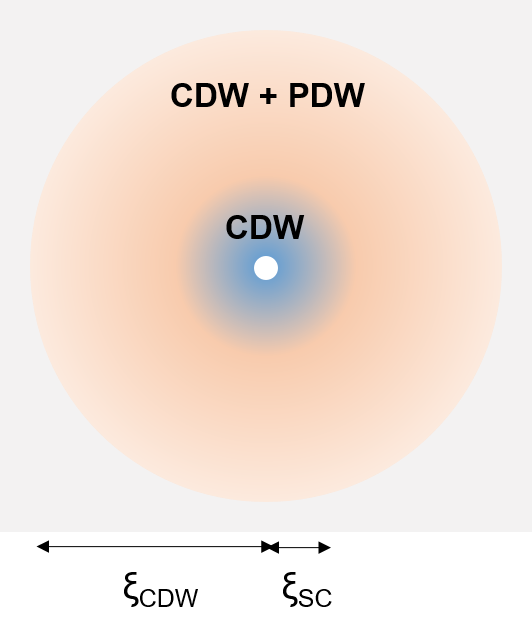
Edkins et al. report that the PDW signature is confined to areas around the vortex cores. To understand why, we must consider the relative strength of the various order parameters. The ordinary superconducting order parameter, , will be completely suppressed at the vortex core, developing its usual value on a lengthscale determined by the penetration depth. Various authors suggest that will appear where is suppressed, although this is not necessary.Wang et al. (2018); Edkins et al. (2019); Agterberg et al. (2020) In Figure 1 we illustrate the consequences of these variations on the observed CDW and PDW signals. A secondary consequence of these effects is that the temperature dependence of the two signals should be different, with the signal at disappearing above , whereas the signal at may persist to a higher temperature.
Here we present details of our investigation of a sample of YBa2Cu3O6.67 (YBCO) using X-ray diffraction to look for the induced pair density wave signal at . This is a different experimental technique to scanning tunnelling microscopy, and so we will discuss briefly what is actually probed in the X-ray diffraction experiment. We will then describe the experimental results.
III What do X-rays actually see?
In our experiment, we use high energy (98.2 keV) X-rays. The X-rays scatter off the overall charge distribution of the electrons in the sample, with contributions from each atom. The contributions from each element have a particular form factor, , determined by the electronic orbital shape and size distribution. For a classical charge density wave, we may consider that there is a spatial variation of charges, independent of the lattice. To describe this from an atomistic starting point, we can consider that the charge associated with a given atom (this can also be thought of as the valence of that atom) may vary in space. In addition to this charge distribution, there will also be a corresponding shift in atomic positions, through electron-phonon coupling. Of course, in a given material, the atomic displacements may occur first, and be followed by a charge distribution.
High energy X-ray diffraction is most sensitive to atomic displacements, as the X-rays will scatter primarily off the large numbers of core electrons associated with the individual atoms, swamping any signature from small charge variations.Chang et al. (2012)
In the picture described in Figure 1, any signal to be observed at will be confined to regions with a correlation length determined by the size of the vortex halo, following the observations of Edkins et al..Edkins et al. (2019) We will therefore only be able to see this signal at high fields (as is also the case for the STM measurements). If we take this correlation length as being Å, we will be able to see the effects of this on the width of the resulting Bragg peak, as it will result in a finite width determined by this correlation length. Edkins et al. have argued that this width should be half that of the signal at (see Figure 1).Edkins et al. (2019) We should expect to see Bragg peaks due to for a large range of momentum transfer values, as this is determined by the underlying atomic form factors.
IV Experimental Methods
We have carried out a high energy X-ray diffraction experiment to look for signs of the CDWs induced by a potential PDW in YBCO. These hard X-ray (98.2 keV) diffraction experiments were carried out at the P07 triple-axis diffractometer at the PETRA-III synchrotron at DESY (Hamburg, Germany). The sample of YBa2Cu3O6.67, with an ortho-VIII structure, has previously been characterized and used in Refs. Chang et al., 2012, 2016). The sample was mounted in a horizontal 17 T cryomagnet.Holmes et al. (2012) The setup was identical to that used in Ref. Chang et al., 2016. The sample was mounted to access either the or scattering planes. A second sample with an ortho-II structure was briefly studied, but not in as much depth, and so we do not present any results here.
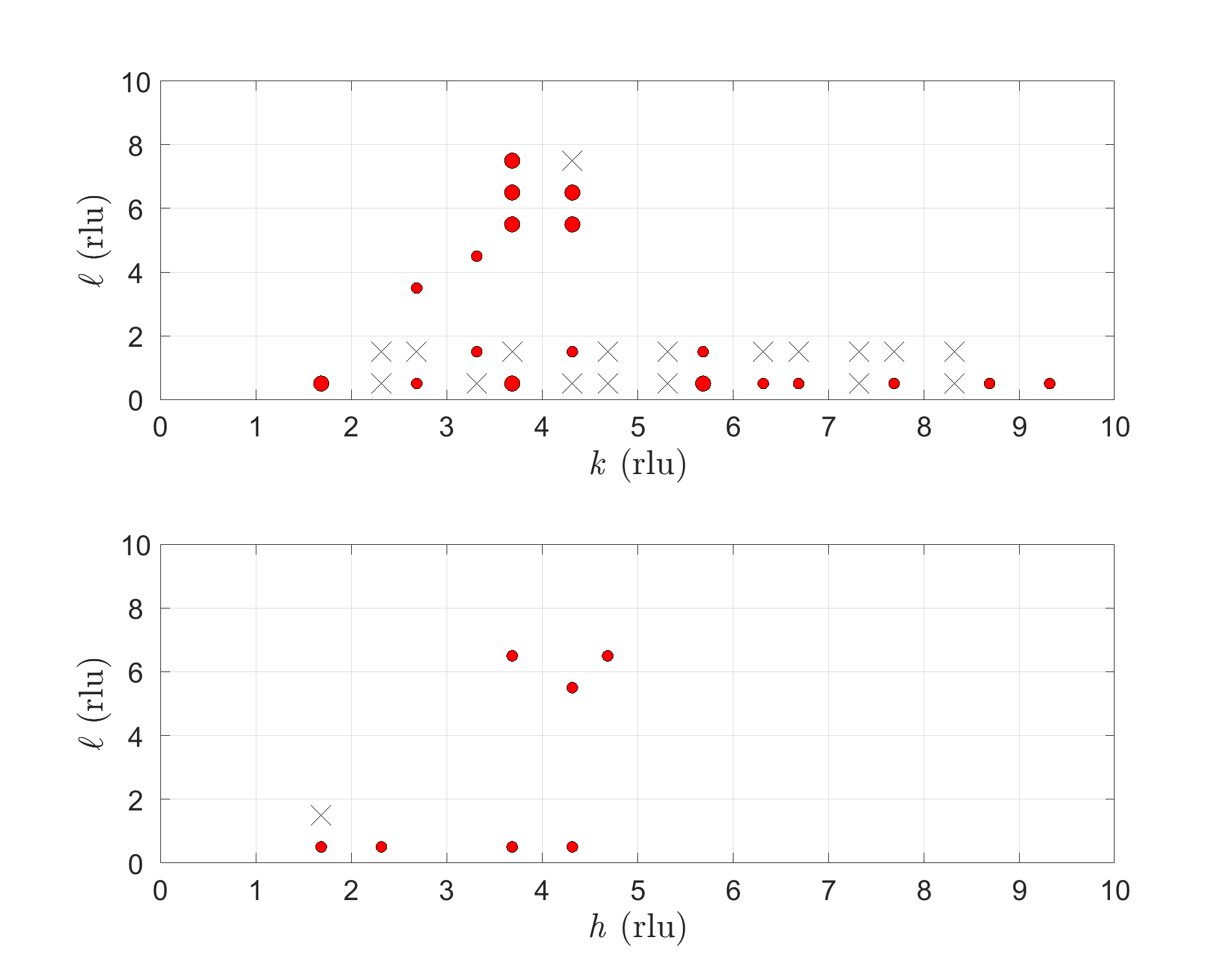
Figure 2 indicates the regions of reciprocal space studied during the experiments, in the (0 K L) and (H 0 L) planes. Although the figure only denotes points at half-integral positions, corresponding to the previously observed CDW wavevectors, measurements were also made at associated integral positions, as well as at a selection of other values. Access to reciprocal space is limited by two conditions. Firstly, if the sample is aligned such that field is parallel to the axis, the opening angles of the cryomagnet restrict the maximum to 20∘. This condition applies to the points measured for . Secondly, the sample may be rotated inside the cryomagnet, such that the field is no longer parallel to the axis. This was done to access the points at higher values. This has the disadvantage of limiting the field along the axis. We measured all of the points accessible with the field along the axis in the (0 K L) plane, and with the sample rotated with respect to the field, we selected points in a region where our previous experimentsForgan et al. (2015) had indicated that the CDW signal was strong.
At certain positions in reciprocal space, our measurements show peaks that come from structured diffuse scattering, as reported by Le Tacon et al.;Le Tacon et al. (2013) a trace of this can be seen in the upper panel of Figure 3. This scattering is identified as such by scanning towards the parent Bragg peak and observing a continual increase.

V Results
We show here data from a subset of the regions studied in Fig. 2, choosing to focus on the data collected close to either or = 2 and . These positions give us the lowest overall magnitude of momentum transfer , and correspond to a strong CDW peak. The results presented here are characteristic of the results obtained at the other positions studied.
Figure 3 gives a broad overview of the data obtained in the plane around the (0 2 0.5) and (0 2 1) positions, in fields from 0 T to 16 T. The charge density wave is observed in its usual position ( = 0.315 Å-1). The charge density wave reflection is visible at 0 T only at (0 2- 0.5), but application of field makes it visible at (0 2+ 0.5), and we can also see the field-induced reflections at = 1 as well. We do not see any sign of increased scattering at the position . The peak seen at (0 2.05 0.5) comes from the structured diffuse scattering noted above. The overall shape of the background scattering is similar to that observed in our previous experiments on multiple samples, see e.g. Forgan et al., 2015.
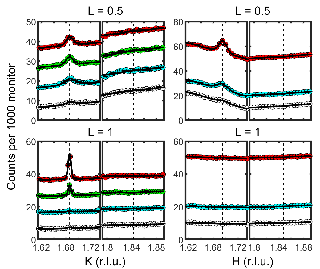
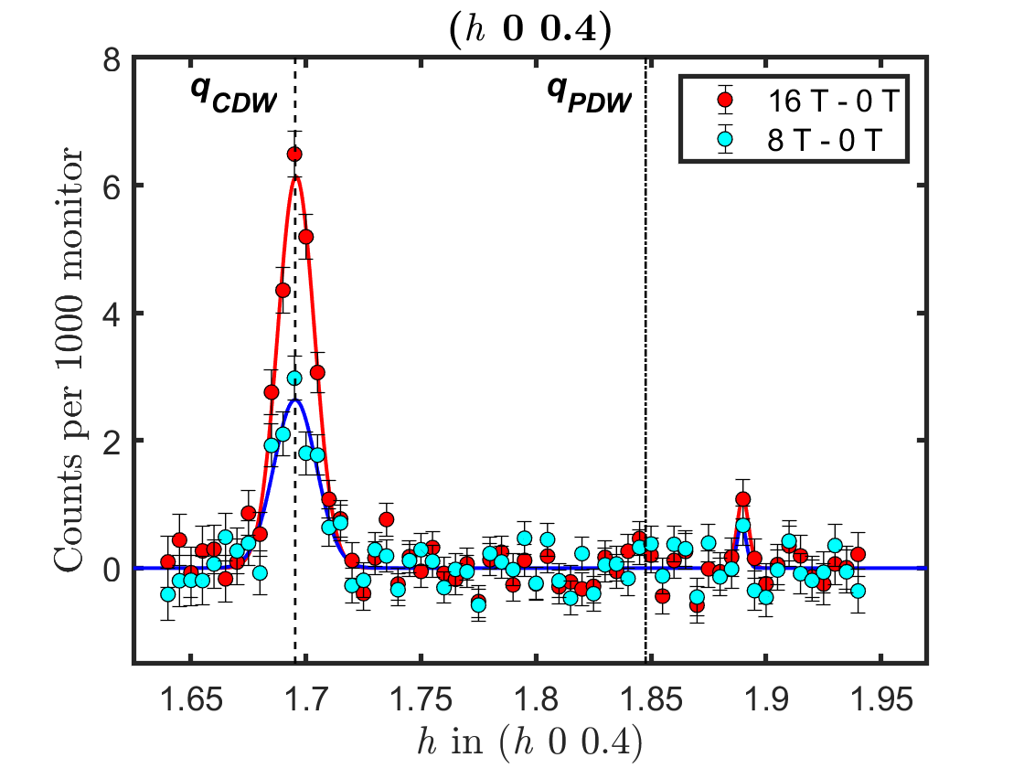
We focus on the data in ranges close to the and positions in Figure 4. This shows linecuts through the CDW and PDW positions in the and directions at = 0.5 and = 1 at fields from 0 T to 16 T, focussing on the (2-) positions. The data have been fitted using a Gaussian function on a sloping background. Where there is no obvious peak, the centre has been set to the expected CDW or PDW value, and the width has been fitted with an upper limit about 20% larger than that observed in the cases where the peaks could be fitted. As expected, for the ( 0 1) case, no high field peak is seen.
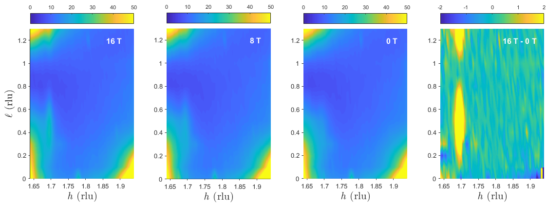
To illustrate that a signal is not appearing at a non-rational value, Figure 5 presents maps in () space, measured at 0 T, 8 T and 16 T, along with the difference between 16 T and 0 T. Here, we see the CDW signal clearly, especially after subtraction, and the background from the primary structural Bragg peaks and the scattering from the Cu-O chains cancels out nicely. Close inspection of the data highlight a couple of additional high points in the subtraction. These are all revealed to be single points high, as illustrated in Figure 6 for the spot appearing at (1.89 0 0.4). We speculate that this is scattering from a micro-crystallite in the sample. Although our sample is detwinned, the detwinning is not perfect (99% detwinned).Chang et al. (2012) The scattering here may be from a small misaligned twin.
VI Discussion
Our experiment shows no evidence for a pair density wave associated with the charge density wave seen in YBCO. This is consistent with observations by Vinograd et al. on YBCO under uniaxial pressure. Vinograd et al. (2023) This could be because there is no pair density wave in this material, but could also arise for several other reasons. As discussed above, the X-rays are looking at atomic positions induced by charge density distributions. This coupling may be too weak in YBCO. The form factor effect may mean that we are too far away in momentum space to see the effect.
The level of coupling between the -wave ”standard” superconducting order parameter and the pair density wave order parameter may be too weak in YBCO. Our results impose limits on the that are quite tight.
In addition, the CDW observed could be an independent order parameter and any PDW/PDW-induced CDW is elsewhere in reciprocal space.
References
- Edkins et al. (2019) S. D. Edkins, A. Kostin, K. Fujita, A. P. Mackenzie, H. Eisaki, S. Uchida, S. Sachdev, M. J. Lawler, E.-A. Kim, J. C. Séamus Davis, and M. H. Hamidian, Science 364, 976 (2019).
- Larkin and Ovchinnikov (1965) A. I. Larkin and Y. N. Ovchinnikov, Sov. Phys. JETP 20, 762 (1965).
- Fulde and Ferrell (1964) P. Fulde and R. A. Ferrell, Physical Review 135, A550 (1964).
- Agterberg et al. (2020) D. F. Agterberg, J. C. Séamus Davis, S. D. Edkins, E. Fradkin, D. J. Van Harlingen, S. A. Kivelson, P. A. Lee, L. Radzihovsky, J. M. Tranquada, and Y. Wang, Annu. Rev. Cond. Matter Physics 11, 231 (2020).
- Tranquada (2013) J. M. Tranquada, in American Institute of Physics Conference Series, American Institute of Physics Conference Series, Vol. 1550, edited by A. Avella and F. Mancini (2013) pp. 114–187, arXiv:1305.4118 [cond-mat.supr-con] .
- Fradkin et al. (2015) E. Fradkin, S. A. Kivelson, and J. M. Tranquada, Reviews of Modern Physics 87, 457 (2015).
- Berg et al. (2009) E. Berg, E. Fradkin, and S. A. Kivelson, Nature Physics 5, 830 (2009).
- Liu et al. (2018) X. Liu, Y. X. Chong, R. Sharma, and J. C. S. Davis, Science 372, 1447 (2021).
- Wang et al. (2018) Y. Wang, S. D. Edkins, M. H. Hamidian, J. C. S. Davis, E. Fradkin, and S. A. Kivelson, Physical Review B 97, 174510 (2018).
- Agterberg and Garaud (2015) D. F. Agterberg and J. Garaud, Phys. Rev. B 91, 104512 (2015).
- Chang et al. (2012) J. Chang, E. Blackburn, A. T. Holmes, N. B. Christensen, J. Larsen, J. Mesot, R. Liang, D. Bonn, W. N. Hardy, A. Watenphul, M. v. Zimmermann, E. M. Forgan, and S. M. Hayden, Nature Physics 8, 871 (2012).
- Chang et al. (2016) J. Chang, E. Blackburn, O. Ivashko, A. T. Holmes, N. B. Christensen, M. Hücker, R. Liang, D. Bonn, W. N. Hardy, U. Rütt, M. v. Zimmermann, E. M. Forgan, and S. M. Hayden, Nature Communications 7, 11494 (2016).
- Holmes et al. (2012) A. T. Holmes, G. R. Walsh, E. Blackburn, E. M. Forgan, and M. Savey-Bennett, Review of Scientific Instruments 83, 023904 (2012).
- Forgan et al. (2015) E. M. Forgan, E. Blackburn, A. T. Holmes, A. K. R. Briffa, J. Chang, L. Bouchenoire, S. D. Brown, R. Liang, D. Bonn, W. N. Hardy, N. B. Christensen, M. v. Zimmermann, M. Hücker, and S. M. Hayden, Nature Communications 6, 10064 (2015).
- Le Tacon et al. (2013) M. Le Tacon, A. Bosak, S. M. Souliou, G. Dellea, T. Loew, R. Heid, K.-P. Bohnen, G. Ghiringhelli, M. Krisch, and B. Keimer, Nature Physics 10, 52 (2013).
- Vinograd et al. (2023) I. Vinograd, S. M. Souliou, A.-A. Haghighirad, T. Lacmann, M. Frachet, M. Merz, N. Maraytta, G. Garbarino, Y. Liu, S. Nakata, K. Ishida, H. M. L. Noad, M. Minola, B. Keimer, C. W. Hicks, and M. L. Tacon, (2023), arXiv:2308.08395 [cond-mat.supr-con] .