Field-Effect Transistors based on 2-D Materials: a Modeling Perspective
1 Introduction
1.1 Future of Moore’s Law
In 1965, Gordon Moore, one of Intel’s co-founders, formulated in 1 his now famous law that states that the number of transistors per integrated circuit (IC) doubles every 18 to 24 months. This miracle has been made possible over the last 50+ years thanks to an aggressive scaling of the dimensions of silicon-based metal-oxide-semiconductor field-effect transistors (MOSFETs), as reviewed in 2. Till 2003, this miniaturization followed Dennar’s scaling law (3), which consisted in reducing the spatial dimensions (width, gate length, oxide thickness) and power supply of every new MOSFET generation by 30%. In other words, these quantities were multiplied by a factor of 0.7 from one generation to the other. As a consequence, the power density of ICs stayed constant over the years, while their performance kept increasing, driven by the shortening of the transistor gate length. Dennard’s scaling stopped however in 2003 at the so-called 130 nm technology node (TN) because the supply voltage of transistors could no more be reduced at the same pace as their dimensions. The sub-threshold slope (), which indicates how rapidly the electrical current of logic switches can be increased between their OFF and ON states explains this phenomenon. In conventional MOSFETs, it is limited to 60 mV/dec at room temperature: the gate voltage must be swept by at least 60 mV to vary the current by one order of magnitude.
The impossibility to push below this limit in MOSFETs forced the semiconductor industry to maintain relatively large supply voltages (above 1 V), thus leading to significant increases of the power and heat dissipation of electronic devices, see 4. At the circuit level, the end of Dennard’s law could be partly compensated by decreasing the clock frequency of ICs to reduce the power dissipation and by combining multiple cores together with shared memory to augment the computational capabilities. This was the beginning of the “multicore crisis”, an on-going era with energy-efficient, parallel, but sequentially slower multicore computers than at the beginning of the 2000’s. At the device level, from 2003 onwards, it was observed that “simply” scaling the size of transistors was no more sufficient to enhance their operation, in particular their switching speed. Since then, different technology boosters have therefore been introduced to ensure that the performance improvements historically brought by Moore’s scaling law could continue, as summarized in 5
-
•
Strain engineering as in 6: from the 90 nm TN, strain has been used in Si MOSFETs to alter the bandstructure of electrons and holes, with an increase of their channel mobility as a result;
-
•
High- oxide layers as in 7: at the 45 nm TN, SiO2, the native oxide of Si, was replaced by high- dielectric layers such as HfO2 that can provide larger gate capacitances together with lower leakage currents;
-
•
3-D FinFETs as in 8: till the 32 nm TN, transistors were 2-D planar structures with a single-gate contact. In 2011, they became 3-D FinFETs with a triple-gate configuration, offering a higher immunity against short-channel effects, in particular source-to-drain tunneling.
The benefits of multicore architectures, strain, high- dielectrics, and FinFETs are best visible in the electronic products that we use on a daily basis, be they cell phones, tablets, or laptops. Quantitatively, these benefits can be assessed by considering the Top500 list of supercomputers available in 9. This list ranks all participating machines based on their performance when running the LINPACK benchmark, see 10. What is measured is the number of floating point operations (Flop) that are processed per second (Flop/s) to solve a linear system of equations on the hardware of interest. Back in 1993 (first Top 500 list), the largest supercomputer in the world achieved 60109 Flop/s, i.e. 60 GFlop/s. Today’s cell phones, with a peak performance larger than 1012 Flop/s (1 TFlop/s), are about 15 to 20 times more powerful than this machine. For its part, the current largest supercomputer in the world, as of November 2020, reaches 4401015 Flop/s (440 PFlop/s), according to 9.
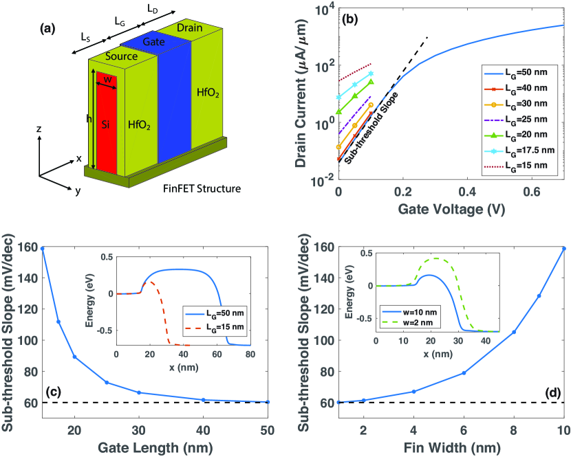
While Si FinFETs have established themselves as the transistors of reference since 2011, they might lose this position in the future, when their gate length will shrink below 15 nm. One of the main challenges associated with the scaling of such devices is illustrated in Fig. 1 using a simplified device structure with realistic dimensions, as schematized in sub-plot (a). At a gate length =50 nm, a fin width of 10 nm together with a fin height of 40 nm yield a subthreshold slope =60.8 mV/dec at room temperature, close to the theoretical limit (sub-plot (b)). If the cross section dimensions are kept the same, but the gate length reduced from 50 to 15 nm, rapidly explodes, reaching 160 mv/dec for the shortest considered , as can be seen in sub-plot (c). The observed deterioration is caused by a loss of electrostatic control, which can be related to a parameter called “natural channel length” and defined in 11 as
| (1) |
where , , , , and are the relative permittivity of Si, that of the oxide layer, the number of gate contacts, the thickness of the Si channel, and that of the oxide surrounding it, respectively. Short-channel effects can be prevented if the gate length is at least 6 larger than . Hence, should be made as small as possible to conveniently scale transistors.
In FinFETs, the number of gate contacts, , is equal to 3. If Si remains the channel material and HfO2 the dielectric of choice, only and can be made thinner. Because decreasing would ultimately lead to high OFF-state gate leakage currents, the only viable solution to scale the of FinFETs appears to be a reduction of , which corresponds to the fin width . This is what has been done in Fig. 1(d). When pushing down to 1 nm, a value of 60 mV/dec can be achieved, which would readily allow to push the gate length of FinFETs (well) below 15 nm, while maintaining a good electrostatics integrity. However, reliably fabricating fin structures with a width of 1 nm only is extremely demanding. Surface roughness, single impurities, or interface traps are all expected to play a non-negligible role at this scale and to negatively impact the Si channel mobility, see 12. Besides these effects, device-to-device variability might become a real issue for ultra-scaled FinFET sizes.
1.2 The Potential of 2-D Materials
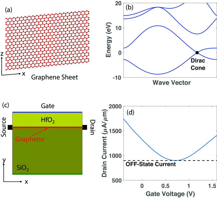
Instead of thinning the width of semiconductors that normally have a 3-D unit cell, 2-D materials with a naturally flat atomic structure might be more promising to create tomorrow’s transistors with a gate length of 15 nm and below (13). Such compounds are characterized by an almost perfect electrostatic control, no surface roughness, and no dangling bonds. Graphene, a carbon monolayer with a honeycomb lattice, is an excellent example of a 2-D material. Its existence was confirmed experimentally in 2004 through mechanical exfoliation, as the dependence of its conductance on an external electric field, see 14. This finding motivated the fabrication of graphene field-effect transistors (GFETs), as in 15, but the absence of a band gap in graphene does not enable to fully switch these devices off, as indicated in Fig. 2. A dispersionless Dirac cone where the conduction and valence bands of touch each other can be noticed in the bandstructure plot, at the -point of the Brillouin Zone. Because of it, the current flow from source to drain can never be completely blocked by the gate-modulated potential barrier, as in Si or III-V MOSFETs.
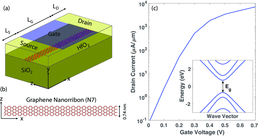
A band gap can be opened up in graphene if it is patterned into a quasi 1-D nanoribbon, either lithographically as in 16 or chemically as in 17. While the former approach is more straightforward to realize, it tends to produce graphene nanoribbons (GNRs) wider than 20 nm whose transport properties suffer from detrimental line edge roughness. The width of chemically-derived GNRs can be reduced below 1 nm with an excellent control of their edges and reproducible electrical characteristics. Transistors made of such 1-D nanostructures can exhibit ON/OFF current ratios greater than 106 as well as ON-state currents in the order of 2000 A/m (18). The simulation of a N7 GNR field-effect transistor (GNRFET) with a width =0.74 nm is shown in Fig. 3 as an example. The investigated logic switch has a gate length =15 nm. It provides a steep sub-threshold slope =67.5 mV/dec, a high ON-current =6.87 mA/m at an OFF-current =74 nA/m and supply voltage =0.7 V. To deliver such a performance, the source and drain extensions of the GNRFET were doped with a donor concentration of 1013 cm-2, which might not be attainable experimentally. Furthermore, it is rather difficult to obtain low contact resistances in GNRFETs and the mass production of ultra-narrow structures is very tedious. Needed are materials that present themselves in the form of relatively easily manufacturable large-scale flakes, as graphene, but that display a band gap compatible with logic applications.
Monolayers of transition metal dichalcogenides (TMD) of composition, where is a transition metal and a chalcogene, fulfill these conditions with their thickness below 1 nm, band gap between 1 and 2 eV, high carrier mobility, and availability as large flakes (19). They are therefore often seen as serious contenders to continue Moore’s scaling law in the “more-than-Moore” category (20). In TMDs, each layer is composed of atoms surrounded by two atoms. The inter-atomic bonds within each layer are covalent, whereas van der Waals forces maintain adjacent layers together in few-layer structures. TMDs can adopt different crystal lattices (and symmetry groups), from the usually semiconducting 2H (hexagonal) phase to the typically metallic 1T (trigonal) or 1T’ (modified trigonal) phase, going through other phases such as 3R (rhombohedral) or 2M (monoclinic). One lattice is generally more stable than the others, but phase transition can be triggered by external fields, strain, or doping, see 21.
Among all existing TMD materials and configurations, single-layer MoS2 was exfoliated for the first time in 1986 with a scotch tape (22), but it was only after the first experimental demonstration in 2011 of a properly working 2H single-gate monolayer MoS2 transistor with =74 mV/dec and an ON/OFF current ratio larger than 108 in 23 that TMD started to receive a wide attention from the scientific community. Since then, transistors with a WSe2 (24), WS2 (25), MoTe2 (26), MoSe2 (27), ReS2 (28), HfSe2, or ZrSe2 (29) channel have been reported as well, to cite few examples. TMD monolayers were used in most cases, except for the MoTe2 (down to 6L), HfSe2, and ZrSe2 (down to 3L) ones, which relied on few-layer structures. Among these 2-D semiconductors, some are better suited to obtain -type transistors, e.g. MoS2, ReS2, HfSe2, or ZrSe2, others lend themselves more naturally to -type devices (WSe2 and MoTe2), whereas MoSe2 is rather ambipolar once crystal defects have been repaired. The type of each TMD is primarily determined by two effects: the metallic contacts attached to it, which affect the Schottky barrier height at the metal-semiconductor interfaces, and the dielectric environment around it, which can transfer electrons or holes to the channel.
The complementary logic at the core of electronic circuits requires both - and -type transistors. Hence, the polarity of 2-D TMDs should be modifiable, which can be done through doping. For instance, a potassium-doped WSe2 channel becomes -type. It can then be combined with a -type WSe2 transistor to give rise to a fully 2-D inverter as in 30. Doping TMDs and more generally 2-D materials remains however a difficult task. Several options exist for that. A back-gate can be inserted to modulate the band edges of the source and drain extensions with respect to the contact Fermi levels (electrostatically-induced doping). Alternatively, ion implantation (31), ion intercalation (32), or charge transfer from, e.g. ionic liquid (33) can be utilized. Nevertheless, none of this approach currently allows to reach doping concentrations as high as in Si.
Apart from doping, TMDs face several other challenges that prevent device engineers from accessing their intrinsic performance and compare it to that of Si FinFETs. One of them is the obtention of high quality, large-scale monolayers. Already in the 1960’s, mechanical exfoliation via scotch tape was applied to isolate layered materials (34). Only small flakes can be gained with this rather straightforward technique, thus hindering mass production of TMD transistors. Lately, impressive progresses have been made with the help of the chemical vapor deposition (CVD) (35) and metal-organic CVD (36), which has been shown to produce large monolayer areas with high carrier mobilities. High-quality TMD flakes in the m2 range can also be generated with atomic layer deposition (ALD) (37).
Other challenges related to the fabrication of high-performance, TMD-based transistors will be discussed in Section 4. As addressing most of them will necessitate significant technology improvements, device simulation can be used in the meantime to provide invaluable insights into the physics of these logic switches, predict their performance limit under ideal conditions, and support the on-going experimental activity. This Chapter will first introduce a suitable modeling approach for that in Section 2 before presenting results of recently undertaken theoretical investigations in Section 3. The latter are not restricted to TMDs, but will also explore novel 2-D semiconductors that could become the channel material of future, ultra-scaled - and -type transistors.
2 Modeling Approach
2.1 Requirements and State-of-the-Art
A critical ingredient of device simulation, regardless of the chosen approach, is the bandstructure of the different materials that constitute the domain of interest. The bandstructure enters either directly or indirectly into the physical model, via the Hamiltonian matrix or the effective mass of the different components, respectively. These quantities are connected through Schrödinger’s equation:
| (2) |
| (3) |
where refers to the electron wave vector, to the wave function of the system at position and wave vector , to the corresponding -dependent band dispersion, and to Planck’s reduced constant. The effective masses are extracted at band extrema that are characterized by the condition . In Figs. 1, 2, and 3, the Hamiltonian matrices of the investigated FinFET, GFET, and GNRFET were constructed in the effective mass approximation (EMA) for Si and in the single- orbital scheme of 38 for graphene. Both models are computationally very attractive, pretty accurate for the systems mentioned above, but unfortunately not ideal for most 2-D materials, as will be explained in the following paragraphs.
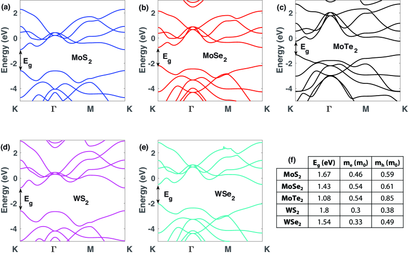
The bandstructure of selected TMDs is shown in Fig. 4, together with their band gap and effective masses. All these quantities were calculated with density-functional theory (DFT), as proposed by 39, an ab initio (from first-principles) method that does not require any input parameters, except for the initial atomic unit cell (AUC) of the material under consideration. This provided AUC is first relaxed so that all atoms occupy stable positions. The corresponding electron density is then self-consistently computed with Poisson’s equation. Finally, all electronic bands are extracted from the obtained DFT Hamiltonian . Although very accurate, DFT still relies on several approximations, among them the exchange-correlation functional, here the PBE one of 40.
What can be clearly seen in Fig. 4 is that the bandstructures of TMDs exhibit complex features such as multiple valleys separated by a small energy interval, strongly non-parabolic bands, and in some cases band anisotropy (the effective masses depend on the crystal orientation). To capture all these effects, a quantum mechanical simulation approach is absolutely necessary. In other words, a Hamiltonian matrix as in Eq. (2) must be assembled to describe the electronic properties of the desired device. On their side, neither classical nor semi-classical methods can shed light on the physics of ultra-thin 2-D materials where electrons and holes are confined over narrow dimensions with dimensions below 0.5 nm. Despite these shortcomings, drift-diffusion calculations can fairly well reproduce experimental data for large-scale TMD flakes, if the available material parameters are properly calibrated (41).
The first quantum mechanical study of a monolayer MoS2 transistor was reported in 42: it was shown that this material could outperform Si as logic switch with a sub-15 nm gate length. To come to this conclusion a quantum transport simulator based on the EMA and the Non-equilibrium Green’s Function (NEGF) formalism proposed by 43 was employed. The functionality of this simulator is similar to the one that produced the data in Fig. 1. We would like to emphasize that NEGF is one of the most popular and powerful techniques to examine charge transport in nanoscale devices. The basic NEGF equations will be reviewed in Section 2.3. At about the same time, a simplified solver based on the straightforward top-of-the-barrier model confirmed these results and revealed that other TMDs might be competitive as well (44). However, because EMA assumes parabolic bands, the satellite conduction band valleys of TMDs could not be properly accounted for in these works. Furthermore, the atomic granularity of single-layer crystals was totally ignored, EMA being continuous.
Device simulators implementing a semi-empirical full-band model represents the next level of accuracy and a significant improvement over the EMA as they include more than a single parabolic band. Hence, the kp as in 45 or tight-binding (TB) method as in 46 or 47 can be used to construct the Hamiltonian matrix of TMDs. As each atom or discretization point is described by a set of orbitals, the simulation time is in the order of times longer than with EMA. Such an increase is still acceptable from a computational point of view because the number of neighbors per point, which determines the band width of the Hamiltonian matrix and the size of the numerical blocks to manipulate, usually remains small. On the negative side, both kp and tight-binding models must be first parameterized, a sometimes tedious operation that is not always successful. Moreover, getting physically meaningful parameters to connect two different materials, e.g. a TMD and the metallic contact attached to it, can be rather complicated. Finally, kp in its usual forms (44 to 88) tends to be restricted to one symmetry point in the Brillouin Zone and does not capture the atomic nature of TMDs.
Going up the ladder, a DFT solver relying on a localized basis set can be coupled to a quantum transport simulator based on the NEGF formalism (48). DFT+NEGF ticks all accuracy boxes (atomistic, full-band, ab initio, capable of treating interfaces and defects, ), but the computational burden of such an approach explodes for large structures composed of several hundreds of atoms. On the one hand, more orbitals per atom are needed. On the other hand, the inter-atomic interactions extends over much longer distances than in tight-binding or kp. In summary, neither , , , nor Hamiltonian matrices are optimal to simulate the electrical behavior of transistors with a 2-D channel material.
2.2 Maximally Localized Wannier Functions (MLWFs)
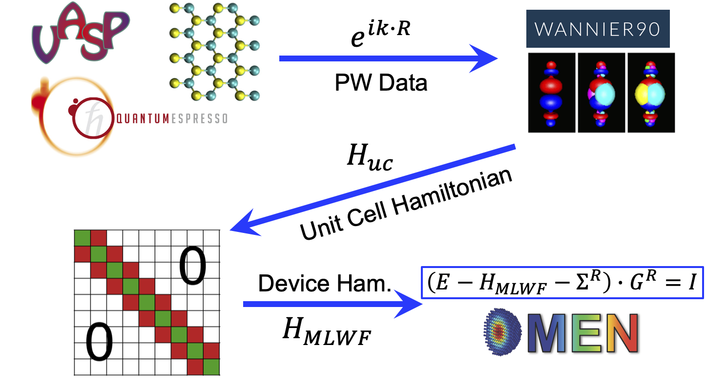
A model that has the same accuracy as DFT and a computational complexity comparable to tight-binding or kp would be ideal to probe 2-D materials as next-generation logic switches. Maximally localized Wannier functions (MLWFs), as introduced by 54, satisfy both conditions, as was first demonstrated in 55 for various TMDs. Since this early work, MLWFs have become very popular among the 2-D research community, as in 56, 57, 58, 59, 60, 61, 62, 63, to mention a few relevant examples. The MLWF method is as accurate as DFT plane-wave (PW) calculations from which they are derived, they require a small number of basis elements per atom, and the distance over which they decay is very short. The numerical treatment of the resulting Hamiltonian matrices, , is therefore facilitated. Thanks to these unique features, MLWFs allow to simulate large transistor structures made of thousands of atoms within reasonable computational times. They can be seen as a first step towards fully ab initio device investigations.
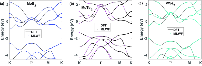
The principle of MLWF-based quantum transport simulations is summarized in Fig. 5. The whole process starts with a plane-wave DFT calculation of a primitive unit cell that best represents the geometry of the targeted atomic system. Different tools such as VASP (49) or Quantum ESPRESSO (50) can be used for that purpose. The produced eigenenergies and eigenvectors are then transformed into a set of MLWFs with the wannier90 package (51). The required unitary transformation is exact so that the bandstructure obtained in the PW and MLWF basis sets are theoretically identical, the only difference being that MLWFs only return a sub-set of all PW bands, in the present case those required to evaluate transport properties. Practically, small discrepancies might emerge due to the truncation of long-ranging interactions. They have a limited impact on the results. As illustrations, the bandstructures of MoS2, MoTe2, and WSe2 are plotted in Fig. 6, as computed with DFT and after a transformation into MLWFs. Excellent agreement between both data sets can be observed.
This PW-to-MLWF conversion gives rise to small Hamiltonian blocks that describe the coupling of the chosen unit cell with itself and with its neighboring cells. Those blocks must be upscaled to form a block tri-diagonal Hamiltonian matrix corresponding to the device to be simulated. Such an upscaling scheme is described in 52. The obtained is perfectly suitable for quantum transport simulations, its increased band width being partly compensated by the fact that less orbitals per atom are required. As a consequence, the same numerical algorithms as with tight-binding can still be employed to solve the NEGF equations. A quantum transport solver such as OMEN (see 53) can do that as it has been specifically designed to handle large-scale nanostructures from first-principles (64). Note that the procedure outlined in Fig. 5 works for any exchange-correlation functional, e.g. the generalized gradient approximation with PBE parameterization (GGA-PBE) of 40, hybrid functionals (HSE06) of 65, or the GW plus Bethe-Salpeter equation (GW-BSE) of 66. The initial DFT run will be longer with HSE06 or GW, but the time for the transport calculation is not affected by this choice.
2.3 Towards Ab Initio Quantum Transport Simulations
In the previous Section, the construction of a MLWF-based Hamiltonian matrix was presented. As last step, should be passed to a quantum transport (QT) solver to perform ab initio device simulations. Various QT methods have been proved effective, among them the solution of the Wigner Transport Equation (67), Pauli’s Master Equation (68), the Quantum Transmitting Boundary Method (QTBM) (69), and, of course, the Non-equilibrium Green’s Function (NEGF) formalism (43) that was already mentioned above. As all results in Section 3 have been obtained with NEGF, the equations governing this transport approach will now be briefly introduced, with emphasis on 2-D material applications.
To describe electron transport within the NEGF framework, the following non-linear system of equations must be solved
| (6) |
In Eq. (6), the ’s represent the electron Green’s Functions. They depend on the electron energy and momentum as well as on the MLWF Hamiltonian matrix . The momentum models the flake direction that is orthogonal to the transport axis and that is assumed periodic. The ’s can be of four different types, retarded (), advanced (), lesser (), or greater (). The ’s refer to the corresponding self-energies where the superscript stands for boundary and for scattering. With , the coupling of the simulation domain with contact electrodes is captured. This self-energy can be computed with so-called decimation techniques (70) or more advanced schemes, for example through eigenvalue problems (71) or contour integrals, as in 72. Its scattering counterpart can include different interaction mechanisms such as electron-phonon, impurity, or interface roughness scattering, see 73.
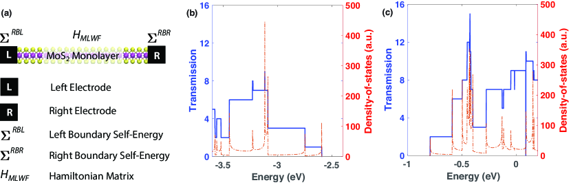
Equation (6) can be efficiently solved with a recursive algorithm that constructs the Green’s Functions from one side of the device to the other in two steps, see 74. In case of ballistic transport, i.e. in the absence of interactions with other carriers, impurities, rough surfaces or crystal vibrations, only the retarded Green’s function needs to be calculated. With its knowledge, both the density-of-states (DOS) and transmission function () of the considered system can be evaluated, from which the carrier density and the electronic current can be derived as in 43. The DOS and of a MoS2 monolayer are provided in Fig. 7 under flat band conditions, evaluated at a single momentum point, =0, for both the conduction and valence bands. The role of and /, the boundary self-energies, is highlighted as well. As expected under such circumstances, the transmission function displays a step-like behavior and effectively counts the number of bands available in the left and right contacts. Each time a transmission channel turns on, the DOS peaks, followed by an exponential decay that is only interrupted by the next peak.
If scattering should be accounted for, the lesser and greater Green’s Functions in Eq. (6) must also be computed. These quantities must be solved self-consistently with the scattering self-energies as they depend on each other. This has been done for example in 75 for single-, double-, and triple-layer MoS2 where electron-phonon scattering was treated at the ab initio level. The same approach was extended in 76 to model self-heating effects and the formation of local hot spots in various field-effect transistors with a TMD monolayer as channel material.
All results presented this Chapter have been obtained in the presence of electron-phonon scattering, but the chosen model relies on a simplified and phenomenological approach with one single phonon energy =40 meV and a scattering strength comprised between 25 and 125 meV (77):
| (7) |
In Eq. (7) is the phonon’s Bose-Einstein distribution function. A dissipative scattering mechanism is needed to avoid a negative differential resistance (NDR) behavior in the - output characteristics of the 2-D FETs, which has never been experimentally observed at room temperature. NDR originates from the bandstructure of 2-D materials, which often exhibits several narrow bands that cannot propagate if the electrostatic potential undergoes large variations from source to drain (78). It is an artifact of the ballistic approximation. The inclusion of electron-phonon scattering helps get rid of this non-physical effect by connecting bands that would otherwise be independent from each other (75). Accounting for the “real” electron-phonon interactions would be more accurate, but gathering the required phonon bandstructures and coupling elements is computationally very demanding, as the self-consistent calculation of the scattering self-energies. For all these reasons, the model of Eq. (7) was adopted.
Finally, it should be noted that all simulations were performed at room temperature with the metal gate work function adjusted so that the OFF-state current is fixed to 0.1 A/m. Perfectly ohmic contacts are assumed (no resistance), except if mentioned otherwise.
3 2-D Device Performance Analysis
3.1 MoS2 and other TMDs
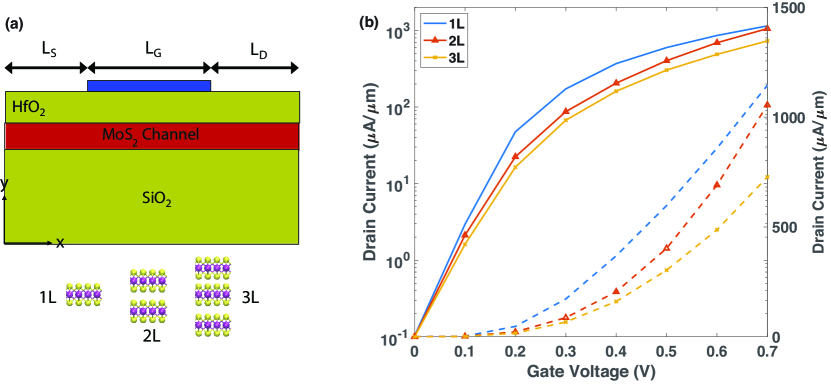
The first 2-D material under the ab initio microscope is MoS2, the TMD whose monolayer form was initially shown to provide excellent transistor characteristics in 23. Before assessing the performance of MoS2 transistors with respect to other 2-D materials, we would like to underline the importance of the channel thickness. In Fig. 8, a simplified device structure is schematized. Its channel is either made of a MoS2 monolayer, bilayer, or trilayer, whose thickness is approximately 0.6, 1.2, and 1.8 nm, respectively. The corresponding transfer characteristics are shown on the right side of the plot. A MLWF Hamiltonian matrix was constructed for each channel configuration. The ab initio simulations reveal that the monolayer structure has the highest ON-state current (1.15 mA/m), followed by the bilayer (1.06 mA/m), and finally the trilayer one (0.73 mA/m). Normally, the opposite order would be expected as the transport effective mass decreases as the number of stacked layers increases. However, the gate contact loses part of its control efficiency at larger channel thicknesses, as already demonstrated in Fig. 1.
This deterioration is best reflected in the value of each transistor, which goes from 68.6 mV/dec in the monolayer case to 75.6 mV/dec in the bilayer and 82.8 mV/dec in the trilayer. The gate contact can very well modulate the height of the potential barrier in the layer that is the closest to it, but its influence decreases as carriers are situated away from it. Hence, the benefit of smaller effective masses in few-layer structures is washed out by the poorer electrostatics of thicker channels. If we compare these results to those of Fig. 1(d), we notice a substantially larger than in the FinFET with a 1-nm wide fin, even for the monolayer FET. The presence of a triple-gate in the FinFET case explains the better scalability of this device. Adding a second gate to the 2-D MoS2 FETs produces the same effect and leads to an almost perfect electrostatic control in mono-, bi- and tri-layer structures down to a gate length =10 nm (75). Note that in this publication, different DFT models were used than here.
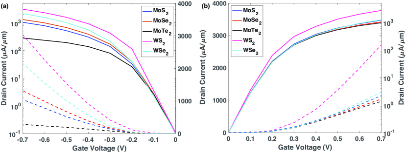
MoS2 has become the most popular TMD, as confirmed by the number of publications dedicated to it, but it is not necessarily the most promising one. Experimentally, no ON-state current larger than 700 A/m has ever been reported for monolayer MoS2 79. This value was obtained at = 5 V, =30 V, and in a device with a gate length =380 nm and an ON/OFF current ratio larger than 106. Other TMDs have therefore also been investigated. The proposed ab initio simulation approach can also be applied to them, as shown in Fig. 6. The MLWF results perfectly reproduces the plane-wave DFT calculations for all TMDs. Taking advantage of that, the transfer characteristics - at =0.7 V of - and -type MoSe2, MoTe2, WS2, and WSe2 field-effect transistors were computed as well. They are displayed in Fig. 9 and compared to those of MoS2. All devices have a structure similar to the one in Fig. 8(a) with a gate length =15 nm and a TMD monolayer as channel material.
First, it can be seen that almost all 2-D FETs have a sub-threshold slope in the order of 70 mV/dec, despite the relatively short and the presence of a single gate contact. There is one exception, WS2, whose is smaller (65 mV/dec). This is not a consequence of a better electrostatic control, but of the influence of narrow energy bands. As explained above, they can lead to the presence of NDR as well as to too low values, even below 60 mV/dec. A physical parameter called “pass factor” allows to quantify the importance of these bands, as explained in 77. The electron-phonon scattering model of Eq. (7) is expected to eliminate these artefacts, but for some 2-D materials, e.g. WS2, it does not fully succeed. Increasing the electron-phonon coupling can improve the situation. However, at the same time, this affects the ON-state current, preventing a fair comparison with other 2-D materials.
The ON-state current values are more broadly distributed than the sub-threshold slopes. Generally, it can be observed that the W-based TMDs perform better than the Mo-based ones, due to lower effective masses and therefore faster carriers, as illustrated in Fig. 4. This trend is not altered if electron-phonon scattering is included because W atoms have a larger mass than Mo’s so that their oscillation amplitude is smaller, as their probability to interact with free carriers (80). Another ab initio theoretical study came to a different conclusion, predicting that the mobility of WS2 would be significantly impacted by electron-phonon scattering (81). The small energy difference between the conduction band minimum of this material and its satellite valleys is the reason behind this discrepancy. As this energy separation strongly depends on the choice of the DFT functional, different calculations might have different outcomes.
| MoS2 | MoSe2 | MoTe2 | WS2 | WSe2 | |
| - (mA/A) | 1.15 | 1.04 | 1.11 | 2.71 | 1.25 |
| - (mV/dec) | 68.6 | 70.1 | 71 | 65.3 | 69.9 |
| - (mA/A) | 1.04 | 1.31 | 0.28 | 3.03 | 2.15 |
| - (mV/dec) | 70.6 | 70 | 70.4 | 66 | 75.2 |
The and of all simulated 2-D TMD FETs are summarized in Table 1. Overall, under ideal conditions, only one 2-D TMD offers an ON-state current significantly larger than 1 mA/m, both in its - and -type configuration, WS2: the -type is 2.71 mA/m, the -type one 3.03 mA/m. Due to the aforementioned issues with the sub-threshold region of these FETs and the possibility that the WS2 mobility might be lower than expected, it must be concluded that 2-D TMDs are probably not the best candidates to replace Si as future, more-than-Moore transistors. Further challenges, but also opportunities to improve their properties will be discussed in Section 4.
3.2 Novel 2-D Materials
Besides TMDs, other 2-D materials suitable for logic applications have emerged over the years, starting with black phosphorus, a monolayer of phosphorus (BP) atoms with a buckled honeycomb lattice (83). Its high hole mobility makes it particularly attractive as -type field-effect transistor, as demonstrated experimentally in 84. While BP has established itself as the most prominent alternative to TMDs, other novel 2-D materials have earned themselves a place under the spotlight, for example silicene in 85, germanene in 86, antimonene in 87, InSe in 88, or Bi2O2Se in 89. Many others are also in the pipeline, see 90, 91.
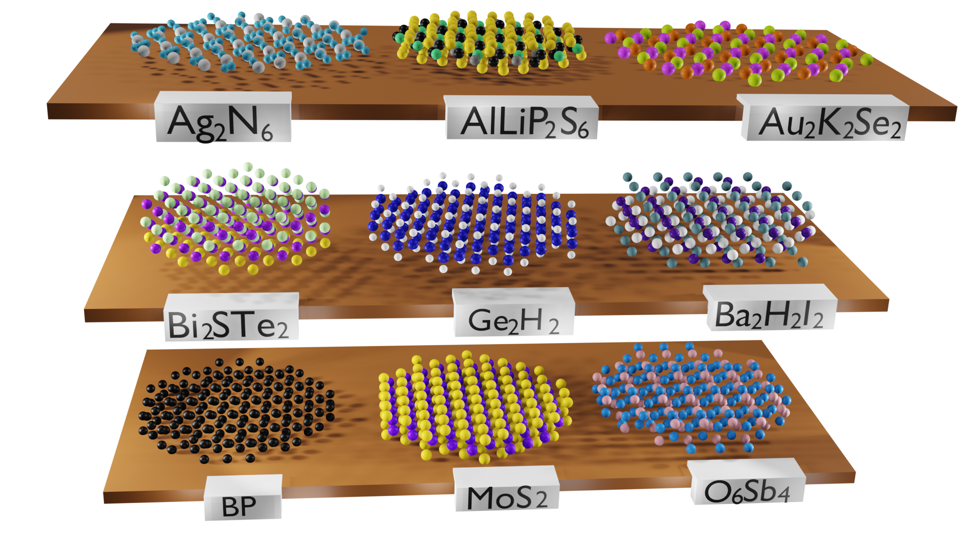
On the theoretical side, a high throughput (HT) investigation by 82 revealed that more than 1,800 2-D materials might exist, among them about 1,000 easily exfoliable monolayers. To come up with these numbers the authors considered a large set of 3-D parent crystals from the Inorganic Crystal Structure Database (ICSD, 92) and the Crystallographic Open Database (COD, 93). They then applied geometrical criteria to identify layered compounds and extract 2-D children from them, tested the stability of the latter in vacuum by computing their phonon bandstructure, and finally classified them according to their inter-layer binding energy and the influence of van der Waals forces. Those of interest have a low and their layers are kept together by non-covalent, van der Waals bonds. All notable 2-D materials (graphene, TMDs, BP, ) were recovered by the HT study of 82. They are accompanied by components with a huge variety of band gaps (from metals to oxides), effective masses (from isotropic to strongly anisotropic bandstructures), and monolayer thicknesses (from one to several repeatable atomic layers). Few examples are proposed in Fig. 10.
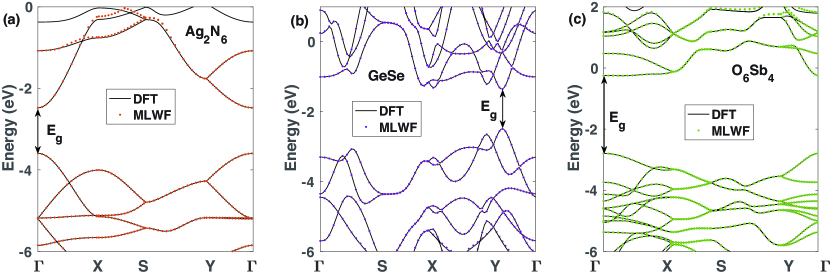
Independently from this study, the potential of 2-D materials beyond TMDs and BP as field-effect transistors has been evaluated through device simulations, with empirical and ab initio models. The related literature is abundant and not all important contributions can be listed here. Nevertheless, the following examples are deemed representative: Bi2O2Se in 94, monochalcogenides in 95, group IV in 96, group V in 58, as well as on more exotic 2-D materials such as Tl2O in 97. To be able to compare the performance of transistors made of these very different 2-D components, a uniform modeling approach would be preferable, for instance the one described in Section 2. It is validated in Fig. 11 for non-conventional 2-D monolayers, Ag2N6, GeSe, and O6Sb4. As for TMDs, the DFT and MLWF bandstructure results agree very well so that everything is in place to conduct a large-scale and systematic performance comparison of 2-D FETs. These results were originally published in 77. All approximations, simulation results, and extracted material parameters are presented in its Supplementary Information.
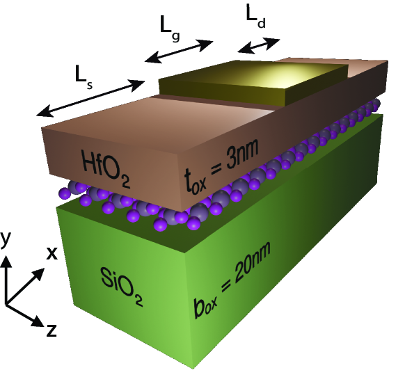
In this context, we designed a realistic 2-D transistor structure, as in Fig. 12, and defined a set of targeted figures of merits (FOM). The dimensions and specifications of this single-gate FET derive inspiration from the International Roadmap for Devices and Systems (IRDS) in 98 for the year 2025, i.e. a gate length =15 nm, a supply voltage =0.7 V, and an equivalent oxide thickness (EOT) of 0.6 nm. This EOT is achieved through a 3 nm HfO2 dielectric layer with a relative permittivity =20. The 2-D materials are deposited onto a SiO2 substrate with a thickness =20 nm and =3.9. To ensure a satisfactory electrostatic control, the source and drain extensions of the FETs are doped with a donor/acceptor concentration =51013 cm-2. Such high values cannot be achieved experimentally for the moment, see 79 or 99, but could be in the future, for example by combining different doping techniques. The SiO2 and HfO2 domains do not enter the NEGF equations, they are treated as perfectly insulating layers that only impact the electric field profile.
In terms of FOM, we are looking for 2-D materials offering an ON-state current larger than 3 mA/m, both in their - and -type configurations, at an OFF-state current =0.1 A/m. At the same time, the sub-threshold slope should not exceed 80 mV/dec at a gate length =15 nm. We selected 100 different 2-D materials from the database of 82 that could potentially reach these objectives. As first criterion, we singled out thin semiconductor monolayers with a small number of atoms in their primitive unit cell (PUC). No compounds thicker that 1.5 nm and with more than 30 atoms in their PUC were considered. Secondly, using the bandstructure calculation results of 82, we further restricted ourselves to 2-D materials with a band gap larger than 1 eV and, if possible, anisotropic conduction band minima and/or valence band maxima so that a low transport and high density-of-states effective mass are simultaneously obtained. Finally, only monolayers that are stable in vacuum were retained, i.e. those whose phonon bandstructure does not have negative branches around the -point.
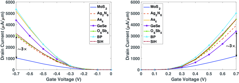
Fig. 13 reports the - and -type transfer characteristics (-) of 6 promising 2-D materials that satisfy the conditions listed above: Ag2N6, As2, GeSe, O6Sb4, black phosphorus (BP), and SiH (silicane). Under ideal conditions, they all deliver 3 mA/m, which is about 3 larger than MoS2, BP even reaching ON-state currents in the order of 5 mA/m. The of all transistors is around 70 mV/dec at =15 nm, which is 10 mV/dec lower than the target that was set. In total, out of the 100 examined 2-D materials, 13 arrive at the desired level of performance. Their FOM and effective masses are summarized in Table 2. None of the conventional TMDs from Fig. 4 (MoS2, MoSe2, MoTe2, WS2, and WSe2) belongs to that group, although WS2 gets very close to it (-type =2.71 mA/m and -type =3.03 mA/m), as can be seen in Table 1. Two less common TMDs, HfS2 and ZrS2, seem to have a higher potential, their - and -type ON-state currents being above 3 mA/m in the ballistic limit of transport.
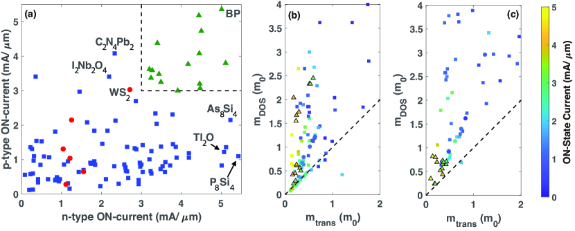
To give an overview of all 2-D materials that have been simulated, we put together their “-type vs. -type ” characteristics in Fig. 14(a). This plot allows to rapidly identify the 13 best-performing candidates as they are situated in the upper right corner delimited by black dashed lines. Overall, several 2-D materials (39) exhibit an ON-state current larger than 3 mA/m in their -type form, e.g. P8Si4 (5.43 mA/m), As8Si4 (5.23 mA/m), or Tl2O (5.09 mA/m), much less (17) as -FET, e.g. C2N4Pb2 (4.08 mA/m) or I2Nb2O4 (3.41 mA/m). As for the Si-based CMOS technology, the fact that more 2-D compounds have a high -type rather than -type ON-state current indicates that fabricating high-performance pFETs might be a challenging task in the flat land as well.

Among all 2-D materials that were simulated, black phosphorus stands out as it displays the largest “-type vs. -type ” combination, when the transport direction of the FET is aligned with the - crystal axis of BP. The conduction and valence band anisotropy of this monolayer (see Fig. 15) is at the origin of the high current densities. Its transport effective mass, , is equal to 0.16 for electrons (0.14 for holes), whereas its density-of-states counterpart, , amounts to 0.42 (0.82 for holes). Other 2-D materials benefit from anisotropic bandstructures, which is the reason why they deliver ’s larger than 3 mA/m, as can be generally seen in Fig. 14(b-c). This is the case of the electrons and holes in Ag2N6, As8Ge4, or As8Si4, and of the holes in I4O4Sc4, for example. Their band extrema have an ellipsoid shape. In fact, almost all 13 best components are characterized by a lower than their , i.e. they are situated above the dashed black lines that correspond to materials with an isotropic bandstructure in Fig. 14(b-c). It should be noted that and were not directly extracted from the bandstructure of the 2-D materials, but by calculating their charge and current densities with analytical equations, as in 77.
The question that arises with materials having an anisotropic conduction band minimum and/or valence maximum is “what happens if the direction along which the electrical current flows is not perfectly aligned with the most suitable crystal axis?”. For example, it is well-known in BP that transport along the - axis is (much) less efficient than along - (100). Using the proposed MLWF+NEGF approach, we found in 101 that orientation misalignments up to from the ideal case do not significantly alter the ON-state current of BP transistors, with almost negligible performance loss up to a misalignment angle of . This means that does not linearly decrease as a function of the misalignment angle, but rather first stays constant up to , slightly decreases up to , and finally rapidly drops. This behavior, which occurs both in the ballistic limit of transport and in the presence of electron/hole-phonon and charged impurity scattering, can be explained by considering the angle-dependent value of the and effective masses.
It is important to realize that the impact of misalignment angles that was discussed above for black phosphorus transistors can be generalized to any 2-D materials with an anisotropic bandstructure. If the ratio of the effective masses extracted from the bandstructure along the two main axes of the Brillouin Zone is smaller than 0.1, i.e. if 10 in Fig. 15, the ON-state current only marginally decreases up to , by if the misalignment is pushed to . It is clear that the magnitude of the ON-state current still depends on the DOS of each 2D material. Nevertheless, a region where the current is almost insensitive to the misalignment angle can be expected in all cases, as suggested 101.
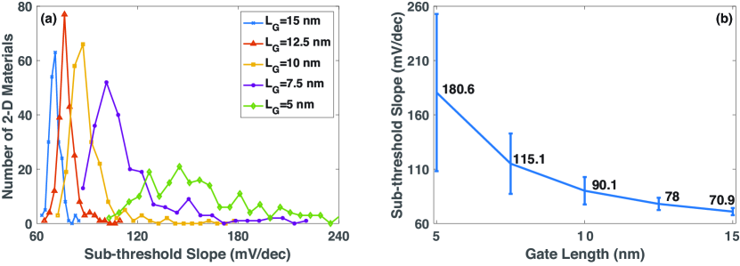
If 2-D materials should replace Si as the channel of future field-effect transistors, they should be used during several consecutive technology nodes. Consequently, it should be possible to scale their gate length and still get a performance superior to that of Si FinFETs or their potential successors, gate-all-around nano-sheets, see 102. Thus, in Fig. 16, we show the sub-threshold slope of all simulated 2-D FETs as histograms for the gate lengths =15, 12.5, 10, 7.5, and 5 nm. The corresponding average values and standard deviations are provided in the right-hand-side of the plot. While slowly increases when shrinks from 15 down to 10 nm, it explodes below 10 nm, as does the variations among the different 2-D materials. From these results, it does not seem feasible to scale single-gate 2-D FETs below 10 nm. By adding a second, symmetric gate at the bottom of the structure in Fig. 12 an improvement of the transistor scalability can be expected. The double-gate architecture is probably the only viable path for 2-D materials to compete with Si FETs. Still, other technology issues remain to be solved, as detailed in the next section. At the same time, new logic switch opportunities could emerge for 2-D materials.
| -FET | -FET | |||||||
| (mA/m) | () | () | (mV/dec) | (mA/m) | () | () | (mV/dec) | |
| Ag2N6 | 3.91 | 0.31 | 0.56 | 67 | 3 | 0.42 | 0.65 | 66.6 |
| As2 | 4.17 | 0.24 | 1.67 | 67.4 | 3.77 | 0.34 | 0.56 | 69.7 |
| As4 | 4.44 | 0.25 | 0.61 | 68.4 | 5.18 | 0.1 | 0.35 | 73.8 |
| Ge2S2 | 4.45 | 0.24 | 0.63 | 67.8 | 4.08 | 0.23 | 0.7 | 65.8 |
| Ge2Se2 | 3.4 | 0.33 | 0.5 | 69.1 | 4.38 | 0.35 | 0.44 | 68 |
| HfS2 | 3.27 | 0.51 | 2.33 | 69.1 | 3.59 | 0.35 | 0.66 | 68.8 |
| O6Sb4 | 4.47 | 0.18 | 2.04 | 67.6 | 3.07 | 0.35 | 0.73 | 62.6 |
| BP | 5.01 | 0.16 | 0.42 | 69.5 | 5.36 | 0.14 | 0.82 | 70.4 |
| Sb2 | 5.11 | 0.23 | 0.55 | 67.5 | 3.8 | 0.3 | 0.52 | 70.1 |
| Si2H2 | 4.46 | 0.29 | 1.74 | 69.5 | 3.2 | 0.43 | 0.71 | 69.5 |
| Ti2Br2N2 | 3.49 | 0.18 | 0.23 | 71.6 | 3.25 | 0.18 | 0.24 | 75.8 |
| Ti2N2Cl2 | 3.44 | 0.22 | 0.29 | 69.9 | 3.48 | 0.19 | 0.24 | 70.4 |
| ZrS2 | 3.24 | 0.59 | 2.45 | 66.4 | 3.37 | 0.37 | 0.7 | 68.5 |
4 Challenges and Opportunities
4.1 Electrical Contacts between Metals and 2-D Monolayers
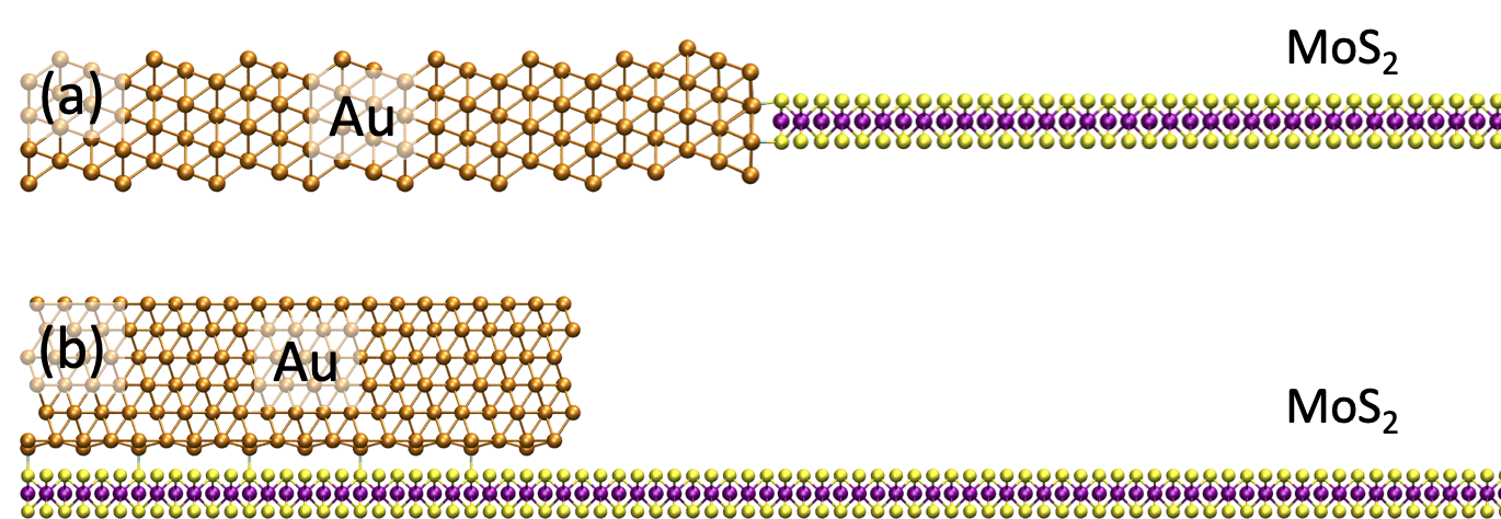
One of the key challenges 2-D materials are facing is their contacting with metallic electrodes. Different approaches can be used to inject electrons into monolayers, the most common ones being top (23), side (103), and phase-engineered contacts (32). The former two are plotted in Fig. 17. Besides these geometries, the choice of the metal (104), the introduction of an interfacial layer between the metal and semiconductor (105), or the doping of the channel (106) represent additional design options. Typically, all these contact configurations are characterized by resistances in the km range (107) instead of 150 to 200 m as in Si FinFETs, see 98. It should nevertheless be mentioned that phase-engineered or nickel-etched graphene electrodes, as in 48, can give lower resistance values, in the order of 200 m, but for multilayer, not monolayer MoS2.
A question that remains open concerns the transfer of electrons from the metallic contact to the semiconductor channel, especially in the case of top-contact architectures. The transfer length measures the average distance that an electron needs to completely leave the metal electrode and enter the semiconducting channel. Two different scenarios are possible, one labeled “edge process” (electrons flow through the metal up to the edge of the metal-semiconductor interface, is close to 0), the other one “area-dependent process” (electrons are gradually transferred from the metal to the semiconductor, 0). For example, in 108, a transfer length nm was found for a monolayer MoS2 with titanium contacts, while in 109 Au electrodes on top of bilayer MoS2 led to low contact resistances =740 m and a short of roughly 30 nm, i.e. a nearly edge process.
On the theoretical side, different explanations for such a behavior have been proposed. Relying on DFT, 110 came to the conclusion that the MoS2 layer below the metallic contact metallizes, which creates an area-dependent injection of electrons. Through device simulations performed in the effective mass approximation, 111 determined that the transfer length depends on the number of layers composing the 2-D material, going from an edge process in monolayers to an area-dependent one in multi-layer compounds. Using our ab initio quantum transport approach, we managed to reconcile these theories. If the metal-semiconductor interface is perfectly clean, the transmission of electrons from the electrode to the channel tends to be edge-dependent in monolayers, while the transfer length increases if an interfacial layer is present between both materials (112). While the exact nature of the transfer process is not yet fully understood, it is clear that should be as small as possible to make the 2-D technology fully scalable. Recently, 113 demonstrated few-layer MoS2 FETs with 13-nm-long top contacts and still very good performance in terms of ON-state current, sub-threshold slope, and contact resistance. These devices have therefore an ultra-short , which goes exactly in the right direction. Note that side contacts are intrinsically more scalable, but they do not currently offer the same performance as top ones, as illustrated in 114.
4.2 2-D Mobility Limiting Factors
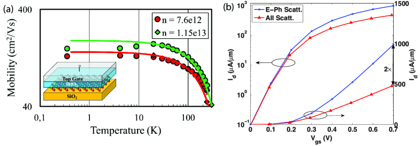
Ab initio calculations have been widely used to predict the phonon-limited mobility of 2-D materials, with a strong focus on TMDs. One of the first such calculations was done in 2012 by 117 for monolayer MoS2. The electron-phonon scattering rates obtained from DFT served as inputs to fit deformation potentials that were then used in a standard linearized Boltzmann Transport Equation (LBTE) solver. A mobility of 410 cm2/Vs at room temperature was returned by this approach. It is much larger than what has been so far measured experimentally, e.g. 63 cm2/Vs at 240 K in 115 or 35.72.6 cm2/Vs at 300 K in 118, depending on the dielectric environment. More recent MoS2 mobility calculations based on fully ab initio electron-phonon scattering rates revealed values much closer to experiments, 150 cm2/Vs in 119 or 144 cm2/Vs in 81. However, other effects such as charged impurity scattering (CIS) (120) or surface optical phonons (SOP) (121) could also play a critical role and bring the mobility closer to measurements.
In Fig. 18(a), we show mobility results for single-layer MoS2 that were computed with our in-house LBTE solver described in 122, including ab initio electron-phonon interactions as well as CIS and SOP. The only parameter that was neither calculated nor taken from the literature is the concentration of charged impurities, . This quantity was used as fitting parameter to best reproduce the experimental data of 115, which was achieved with =2.51012 cm-2. An excellent agreement between simulations and experiments is obtained for two different electron concentrations, 7.61012 and 1.151013 cm-2.
Getting the mobility gives a lot of information about the transport properties of a material, but being able to determine the influence of this figure of merit on the “current vs. voltage” characteristics of a device is equally important. To do that, we used our LBTE solver to calibrate the magnitude of the scattering mechanisms in our MLWF+NEGF QT simulator, OMEN (116). This step is necessary as several approximations to the scattering self-energies must be applied in the NEGF formalism. To compensate for them, each scattering rate (electron-phonon, CIS, and SOP) can be scaled by a different factor so that both LBTE and QT produce the same mobility. This is what we did for a MoS2 monolayer before simulating the transfer characteristics of a device similar to the one in Fig. 8(a). Results are presented in Fig. 18(b), where the currents with electron-phonon scattering only and with additionally CIS and SOP are compared to each other. It can be seen that CIS and SOP, together, are responsible for a reduction of the ON-state current by a factor 2, as compared to the case without them so that does not exceed 500 A/m at a gate length =15 nm. This finding indicates that there is room for improvement. The impurity concentration might indeed be decreased by improving the 2-D crystal quality and its interface with the dielectric environment, while SOP might be minimized through substrate engineering. Furthermore, strain might have a beneficial impact on the electronic properties of MoS2, as theoretically demonstrated in 123 for other 2-D materials. Overall, there are certainly multiple paths to push the ON-state current of MoS2 above 1 mA/m.
4.3 2-D Oxides
What has made silicon such an attractive channel material for transistors is the existence of a native oxide, SiO2, that can be used to separate it from gate contacts or from another dielectric layer. Although not perfect, the Si-SiO2 interface contains a low defect density, contrary to what is found if SiO2, Al2O3, or HfO2 is deposited on a TMD monolayer, see 124. There are few exceptions such as ZrO2 on ZrSe2 or HfO2 on HfSe2: although large ON/OFF current ratios were demonstrated, the extracted carrier mobilities remained small and the I-V characteristics still exhibited an hysteresis (29) when sweeping the gate voltage back and forth. Such a behavior is usually induced by the presence of interface traps that are charged and discharged as the gate potential varies.
Another approach consists of placing a 2-D oxide on a 2-D channel material. The most common 2-D insulator is hexagonal boron nitride (hBN). For example, encapsulating MoS2 between hBN layers has been shown to produce higher mobility values, both in mono- and few-layer configurations (125). Using hBN in transistor applications might however not be optimal as the relative dielectric permittivity, , of this materials is in the order of 5. To reach an EOT of 1 nm or less, a hBN thickness of 1.3 nm is needed, which corresponds to 3 to 4 layers. We used our ab initio QT simulator to determine what the implications of such thin oxides might be for gate leakage currents (126). As testbed, a Au-hBN-Si metal-oxide-semiconductor (MOS) capacitor was constructed at the atomic level and the current that flows through it computed as a function of the applied voltage. It was found that 3 and 4 layers of hBN are not sufficient to satisfy the IRDS requirements. The situation dramatically worsens if a defect is present in the hBN dielectric. Bridges can form between adjacent hBN layers, which locally increases the leakage current, as can be seen in Fig. 19. All current trajectories converge towards the defect location.
Other 2-D oxides have been deposited on TMD channels, e.g. CaF2 in 127. The advantages of such crystals are that they have a perfectly ordered structure, contrary to SiO2 or HfO2, which are amorphous, and that they form a quasi van der Waals interface with 2-D channels. Furthermore, the dielectric constant of CaF2 is higher than that of hBN such that 2 nm of this oxide yields an EOT of roughly 1 nm. Given the fact that the 2-D material space includes more than 1,800 compounds (82), it can be expected that several other 2-D oxides might be exfoliated in the future and that some of them are competitive with HfO2 in terms of and band offsets, while preserving clean oxide-semiconductor interface.
4.4 Advanced Logic Concepts
2-D materials do not only face challenges, they also offer opportunities in advanced logic applications. Their excellent electrostatic control properties are particularly appealing for the realization of band-to-band tunneling field-effect transistors (TFETs). An entire chapter of this book is dedicated to these logic concepts that could theoretically exhibit a sub-threshold slope below 60 mV/dec at room temperature (129). Such a feature enables for a drastic reduction of the supply voltage and therefore of the power consumption of integrated circuits. However, due to the tunneling nature of the injection mechanism, TFETs tend to suffer from very low ON-state currents. Typically, a large band gap is needed to ensure a steep and a low , while a small band gap is necessary to boost . This dichotomy can be partly addressed through the usage of heterojunctions, as demonstrated in 130.
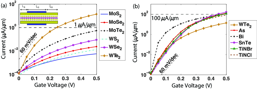
Through device simulation, it has been shown in 131 and 132 that conventional TMD monolayers are probably not the best TFET candidates as their large band gaps do not allow the ON-state current to reach large values. This behavior is confirmed in Fig. 20(a): if the OFF-state current is fixed to 0.1 nA/m and the supply voltage to 0.5 V, does not exceed 1 A/m, except for WTe2, a TMD that is rather difficult to stabilize in the 2H phase. Even worse, the is superior to 60 mV/dec for several of the considered TMDs. This can be explained by the fact that even in the OFF-state, the tunneling channel is already open, i.e. the conduction band below the gate contact has already been pushed below the valence band of the source, see 128. Once this condition is satisfied, the increase with respect slows down and becomes almost linear instead of exponential.
There are different solutions to obtain a better TFET performance, for example by combining different TMDs and forming van der Waals heterostructures. The benefit of such approaches has been highlighted both theoretically in 133, 57, or 134 and experimentally in 135, 136, or 137 combining different TMDs together or one TMD with another material, e.g. germanium. Alternatively, the huge variety of properties encountered in 2-D materials (see 82) can be taken advantage of to identify compounds with low band gaps, compatible with a high ON-state current. With the help of our MLWF+NEGF solver, we have simulated the electrical behavior of relevant examples. Their transfer characteristics are displayed in Fig. 20(b). All have ’s in the order of 100 A/m at =0.5 V and =0.1 nA/m, which is 100 larger than most TMDs. At the same time, a steep is obtained. Further investigations would be needed to screen the available design space, which may contain many more 2-D materials with band gaps comprised between 0.5 and 1 eV.
5 Conclusion and Outlook
In this Chapter, the potential of 2-D materials as field-effect transistors has been discussed from a modeling perspective, starting from the key features of monolayers. The importance of being able to simulate their electrical characteristics has been introduced. Among all possible approaches, the combination of plane-wave density functional theory, maximally localized Wannier functions, and quantum transport has been selected for its versatility and accuracy. By applying it, it has been revealed that transition metal dichalcogenides cannot currently provide a switching performance that is comparable to that of Si FinFETs. They suffer from technical difficulties that will probably disappear with time, such as their electrical contacting, as well as from inherent deficiencies, e.g. relative large effective masses that negatively impact their carrier mobilities. We have shown theoretically that novel 2-D materials represent an attractive alternative to TMDs with excellent figures of merits as logic switches. It remains to confirm experimentally the predicted performance, which requires first to isolate the desired mono- or few-layer components.
6 Acknowledgment
The work presented in this Chapter was supported by ETH Zurich (grant ETH-32 15-1) and by the Swiss National Science Foundation (SNSF) under grant no. 200021_175479 (ABIME) and under the NCCR MARVEL. We acknowledge PRACE for awarding us access to Piz Daint at CSCS under Project pr28, PRACE for the allocated computational resources on Marconi at CINECA under Project 2016163963, and CSCS for Project s876.
References
- Moore 2006 Moore, G. E. Cramming more components onto integrated circuits, Reprinted from Electronics, volume 38, number 8, April 19, 1965, pp.114 ff. IEEE Solid-State Circuits Society Newsletter 2006, 11, 33–35
- Khan et al. 2018 Khan, H. N.; Hounshell, D. A.; Fuchs, E. R. H. Science and research policy at the end of Moore’s law. Nature Electronics 2018, 1, 14–21
- Dennard et al. 1974 Dennard, R. H.; Gaensslen, F. H.; Yu, H.; Rideout, V. L.; Bassous, E.; LeBlanc, A. R. Design of ion-implanted MOSFET’s with very small physical dimensions. IEEE Journal of Solid-State Circuits 1974, 9, 256–268
- Pop et al. 2006 Pop, E.; Sinha, S.; Goodson, K. E. Heat Generation and Transport in Nanometer-Scale Transistors. Proceedings of the IEEE 2006, 94, 1587–1601
- Kuhn 2012 Kuhn, K. J. Considerations for Ultimate CMOS Scaling. IEEE Transactions on Electron Devices 2012, 59, 1813–1828
- Thompson et al. 2002 Thompson, S. et al. A 90 nm logic technology featuring 50 nm strained silicon channel transistors, 7 layers of Cu interconnects, low k ILD, and 1 /spl mu/m/sup 2/ SRAM cell. Digest. International Electron Devices Meeting,. 2002; pp 61–64
- Mistry et al. 2007 Mistry, K. et al. A 45nm Logic Technology with High-k+Metal Gate Transistors, Strained Silicon, 9 Cu Interconnect Layers, 193nm Dry Patterning, and 100% Pb-free Packaging. 2007 IEEE International Electron Devices Meeting. 2007; pp 247–250
- Hisamoto et al. 1998 Hisamoto, D.; Wen-Chin Lee; Kedzierski, J.; Anderson, E.; Takeuchi, H.; Asano, K.; Tsu-Jae King; Bokor, J.; Chenming Hu A folded-channel MOSFET for deep-sub-tenth micron era. International Electron Devices Meeting 1998. Technical Digest. 1998; pp 1032–1034
- top 2020 Top500: TOP 500 Supercomputer Sites. 2020; \urlhttp://www.top500.org
- Dongarra et al. 2003 Dongarra, J. J.; Luszczek, P.; Petitet, A. The LINPACK Benchmark: past, present and future. Concurrency and Computation: Practice and Experience 2003, 15, 803–820
- Appenzeller et al. 2008 Appenzeller, J.; Knoch, J.; Bjork, M. T.; Riel, H.; Schmid, H.; Riess, W. Toward Nanowire Electronics. IEEE Transactions on Electron Devices 2008, 55, 2827–2845
- Uchida et al. 2007 Uchida, K.; Koga, J.; Takagi, S.-i. Experimental study on electron mobility in ultrathin-body silicon-on-insulator metal-oxide-semiconductor field-effect transistors. Journal of Applied Physics 2007, 102, 074510
- Fiori et al. 2014 Fiori, G.; Bonaccorso, F.; Iannaccone, G.; Palacios, T.; Neumaier, D.; Seabaugh, A.; Banerjee, S. K.; Colombo, L. Electronics based on two-dimensional materials. Nature Nanotechnology 2014, 9, 768–779
- Novoselov et al. 2004 Novoselov, K. S.; Geim, A. K.; Morozov, S. V.; Jiang, D.; Zhang, Y.; Dubonos, S. V.; Grigorieva, I. V.; Firsov, A. A. Electric Field Effect in Atomically Thin Carbon Films. Science 2004, 306, 666–669
- Lemme et al. 2007 Lemme, M. C.; Echtermeyer, T. J.; Baus, M.; Kurz, H. A Graphene Field-Effect Device. IEEE Electron Device Letters 2007, 28, 282–284
- Han et al. 2007 Han, M. Y.; Özyilmaz, B.; Zhang, Y.; Kim, P. Energy Band-Gap Engineering of Graphene Nanoribbons. Phys. Rev. Lett. 2007, 98, 206805
- Cai et al. 2010 Cai, J.; Ruffieux, P.; Jaafar, R.; Bieri, M.; Braun, T.; Blankenburg, S.; Muoth, M.; Seitsonen, A. P.; Saleh, M.; Feng, X.; Müllen, K.; Fasel, R. Atomically precise bottom-up fabrication of graphene nanoribbons. Nature 2010, 466, 470–473
- Wang et al. 2008 Wang, X.; Ouyang, Y.; Li, X.; Wang, H.; Guo, J.; Dai, H. Room-Temperature All-Semiconducting Sub-10-nm Graphene Nanoribbon Field-Effect Transistors. Phys. Rev. Lett. 2008, 100, 206803
- Akinwande et al. 2019 Akinwande, D.; Huyghebaert, C.; Wang, C.-H.; Serna, M. I.; Goossens, S.; Li, L.-J.; Wong, H.-S. P.; Koppens, F. H. L. Graphene and two-dimensional materials for silicon technology. Nature 2019, 573, 507–518
- Schwierz et al. 2015 Schwierz, F.; Pezoldt, J.; Granzner, R. Two-dimensional materials and their prospects in transistor electronics. Nanoscale 2015, 7, 8261–8283
- Duerloo et al. 2014 Duerloo, K.-A. N.; Li, Y.; Reed, E. J. Structural phase transitions in two-dimensional Mo- and W-dichalcogenide monolayers. Nature Communications 2014, 5, 4214
- Joensen et al. 1986 Joensen, P.; Frindt, R.; Morrison, S. Single-layer MoS2. Materials Research Bulletin 1986, 21, 457–461
- Radisavljevic et al. 2011 Radisavljevic, B.; Radenovic, A.; Brivio, J.; Giacometti, V.; Kis, A. Single-layer MoS2 transistors. Nature Nanotechnology 2011, 6, 147–150
- Fang et al. 2012 Fang, H.; Chuang, S.; Chang, T. C.; Takei, K.; Takahashi, T.; Javey, A. High-Performance Single Layered WSe2 p-FETs with Chemically Doped Contacts. Nano Letters 2012, 12, 3788–3792
- Ovchinnikov et al. 2014 Ovchinnikov, D.; Allain, A.; Huang, Y.-S.; Dumcenco, D.; Kis, A. Electrical Transport Properties of Single-Layer WS2. ACS Nano 2014, 8, 8174–8181
- Fathipour et al. 2014 Fathipour, S.; Ma, N.; Hwang, W. S.; Protasenko, V.; Vishwanath, S.; Xing, H. G.; Xu, H.; Jena, D.; Appenzeller, J.; Seabaugh, A. Exfoliated multilayer MoTe2 field-effect transistors. Applied Physics Letters 2014, 105, 192101
- Meng et al. 2017 Meng, Y.; Ling, C.; Xin, R.; Wang, P.; Song, Y.; Bu, H.; Gao, S.; Wang, X.; Song, F.; Wang, J.; Wang, X.; Wang, B.; Wang, G. Repairing atomic vacancies in single-layer MoSe2 field-effect transistor and its defect dynamics. npj Quantum Materials 2017, 2, 16
- Liu et al. 2015 Liu, E. et al. Integrated digital inverters based on two-dimensional anisotropic ReS2 field-effect transistors. Nature Communications 2015, 6, 6991
- Mleczko et al. 2017 Mleczko, M. J.; Zhang, C.; Lee, H. R.; Kuo, H.-H.; Magyari-Köpe, B.; Moore, R. G.; Shen, Z.-X.; Fisher, I. R.; Nishi, Y.; Pop, E. HfSe2 and ZrSe2: Two-dimensional semiconductors with native high- oxides. Science Advances 2017, 3
- Tosun et al. 2014 Tosun, M.; Chuang, S.; Fang, H.; Sachid, A. B.; Hettick, M.; Lin, Y.; Zeng, Y.; Javey, A. High-Gain Inverters Based on WSe2 Complementary Field-Effect Transistors. ACS Nano 2014, 8, 4948–4953
- Suh et al. 2018 Suh, J. et al. Reconfiguring crystal and electronic structures of MoS2 by substitutional doping. Nature Communications 2018, 9, 199
- Kappera et al. 2014 Kappera, R.; Voiry, D.; Yalcin, S. E.; Branch, B.; Gupta, G.; Mohite, A. D.; Chhowalla, M. Phase-engineered low-resistance contacts for ultrathin MoS2 transistors. Nature Materials 2014, 13, 1128–1134
- Allain and Kis 2014 Allain, A.; Kis, A. Electron and Hole Mobilities in Single-Layer WSe2. ACS Nano 2014, 8, 7180–7185
- F. and D. 1963 F., F. R.; D., Y. A. Physical properties of layer structures : optical properties and photoconductivity of thin crystals of molybdenum disulphide. Proc. R. Soc. Lond. 1963, 273, A27369–83
- Najmaei et al. 2013 Najmaei, S.; Liu, Z.; Zhou, W.; Zou, X.; Shi, G.; Lei, S.; Yakobson, B. I.; Idrobo, J.-C.; Ajayan, P. M.; Lou, J. Vapour phase growth and grain boundary structure of molybdenum disulphide atomic layers. Nature Materials 2013, 12, 754–759
- Kang et al. 2015 Kang, K.; Xie, S.; Huang, L.; Han, Y.; Huang, P. Y.; Mak, K. F.; Kim, C.-J.; Muller, D.; Park, J. High-mobility three-atom-thick semiconducting films with wafer-scale homogeneity. Nature 2015, 520, 656–660
- Balasubramanyam et al. 2020 Balasubramanyam, S.; Merkx, M. J. M.; Verheijen, M. A.; Kessels, W. M. M.; Mackus, A. J. M.; Bol, A. A. Area-Selective Atomic Layer Deposition of Two-Dimensional WS2 Nanolayers. ACS Materials Letters 2020, 2, 511–518
- Wallace 1947 Wallace, P. R. The Band Theory of Graphite. Phys. Rev. 1947, 71, 622–634
- Kohn and Sham 1965 Kohn, W.; Sham, L. J. Self-Consistent Equations Including Exchange and Correlation Effects. Phys. Rev. 1965, 140, A1133–A1138
- Perdew et al. 1996 Perdew, J. P.; Burke, K.; Ernzerhof, M. Generalized Gradient Approximation Made Simple. Phys. Rev. Lett. 1996, 77, 3865–3868
- Knobloch et al. 2017 Knobloch, T.; Rzepa, G.; Illarionov, Y. Y.; Waltl, M.; Schanovsky, F.; Jech, M.; Stampfer, B.; Furchi, M. M.; Müller, T.; Grasser, T. Physical modeling of the hysteresis in M0S2 transistors. 2017 47th European Solid-State Device Research Conference (ESSDERC). 2017; pp 284–287
- Yoon et al. 2011 Yoon, Y.; Ganapathi, K.; Salahuddin, S. How Good Can Monolayer MoS2 Transistors Be? Nano Letters 2011, 11, 3768–3773
- Datta 1995 Datta, S. Electronic Transport in Mesoscopic Systems; Cambridge Studies in Semiconductor Physics and Microelectronic Engineering; Cambridge University Press, 1995
- Liu et al. 2011 Liu, L.; Kumar, S. B.; Ouyang, Y.; Guo, J. Performance Limits of Monolayer Transition Metal Dichalcogenide Transistors. IEEE Transactions on Electron Devices 2011, 58, 3042–3047
- Kormányos et al. 2015 Kormányos, A.; Burkard, G.; Gmitra, M.; Fabian, J.; Zólyomi, V.; Drummond, N. D.; Fal’ko, V. k p theory for two-dimensional transition metal dichalcogenide semiconductors. 2D Materials 2015, 2, 022001
- Zahid et al. 2013 Zahid, F.; Liu, L.; Zhu, Y.; Wang, J.; Guo, H. A generic tight-binding model for monolayer, bilayer and bulk MoS2. AIP Advances 2013, 3, 052111
- Ilatikhameneh et al. 2015 Ilatikhameneh, H.; Tan, Y.; Novakovic, B.; Klimeck, G.; Rahman, R.; Appenzeller, J. Tunnel Field-Effect Transistors in 2-D Transition Metal Dichalcogenide Materials. IEEE Journal on Exploratory Solid-State Computational Devices and Circuits 2015, 1, 12–18
- Leong et al. 2015 Leong, W. S.; Luo, X.; Li, Y.; Khoo, K. H.; Quek, S. Y.; Thong, J. T. L. Low Resistance Metal Contacts to MoS2 Devices with Nickel-Etched-Graphene Electrodes. ACS Nano 2015, 9, 869–877
- Kresse and Furthmüller 1996 Kresse, G.; Furthmüller, J. Efficiency of ab-initio total energy calculations for metals and semiconductors using a plane-wave basis set. Computational Materials Science 1996, 6, 15–50
- Giannozzi et al. 2009 Giannozzi, P. et al. QUANTUM ESPRESSO: a modular and open-source software project for quantum simulations of materials. Journal of Physics: Condensed Matter 2009, 21, 395502
- Mostofi et al. 2008 Mostofi, A. A.; Yates, J. R.; Lee, Y.-S.; Souza, I.; Vanderbilt, D.; Marzari, N. wannier90: A tool for obtaining maximally-localised Wannier functions. Computer Physics Communications 2008, 178, 685–699
- Stieger and Luisier 2020 Stieger, C.; Luisier, M. Winterface: An Interface from Wannier90 to Quantum Transport. 2020
- Brück et al. 2017 Brück, S.; Calderara, M.; Bani-Hashemian, M. H.; VandeVondele, J.; Luisier, M. Efficient algorithms for large-scale quantum transport calculations. The Journal of Chemical Physics 2017, 147, 074116
- Marzari and Vanderbilt 1997 Marzari, N.; Vanderbilt, D. Maximally localized generalized Wannier functions for composite energy bands. Phys. Rev. B 1997, 56, 12847–12865
- Chang et al. 2014 Chang, J.; Register, L. F.; Banerjee, S. K. Ballistic performance comparison of monolayer transition metal dichalcogenide MX2 (M = Mo, W; X = S, Se, Te) metal-oxide-semiconductor field effect transistors. Journal of Applied Physics 2014, 115, 084506
- Bruzzone et al. 2014 Bruzzone, S.; Iannaccone, G.; Marzari, N.; Fiori, G. An Open-Source Multiscale Framework for the Simulation of Nanoscale Devices. IEEE Transactions on Electron Devices 2014, 61, 48–53
- Szabó et al. 2015 Szabó, A.; Koester, S. J.; Luisier, M. Ab-Initio Simulation of van der Waals MoTe2-SnS2 Heterotunneling FETs for Low-Power Electronics. IEEE Electron Device Letters 2015, 36, 514–516
- Pizzi et al. 2016 Pizzi, G.; Gibertini, M.; Dib, E.; Marzari, N.; Iannaccone, G.; Fiori, G. Performance of arsenene and antimonene double-gate MOSFETs from first principles. Nature Communications 2016, 7, 12585
- Lu et al. 2017 Lu, A. K. A.; Pourtois, G.; Luisier, M.; Radu, I. P.; Houssa, M. On the electrostatic control achieved in transistors based on multilayered MoS2: A first-principles study. Journal of Applied Physics 2017, 121, 044505
- Wang et al. 2016 Wang, K.; Valencia, D.; Charles, J.; He, Y.; Povolotskyi, M.; Klimeck, G.; Maassen, J.; Lundstrom, M.; Kubis, T. NEMO5: Predicting MoS2 heterojunctions. 2016 International Conference on Simulation of Semiconductor Processes and Devices (SISPAD). 2016; pp 221–224
- AlMutairi et al. 2018 AlMutairi, A.; Yin, D.; Yoon, Y. PtSe2 Field-Effect Transistors: New Opportunities for Electronic Devices. IEEE Electron Device Letters 2018, 39, 151–154
- Dong and Littlewood 2019 Dong, W.; Littlewood, P. B. Quantum Electron Transport in Ohmic Edge Contacts between Two-Dimensional Materials. ACS Applied Electronic Materials 2019, 1, 799–803
- Afzalian 2021 Afzalian, A. Ab initio perspective of ultra-scaled CMOS from 2D-material fundamentals to dynamically doped transistors. npj 2D Materials and Applications 2021, 5, 5
- Calderara et al. 2015 Calderara, M.; Brück, S.; Pedersen, A.; Bani-Hashemian, M. H.; VandeVondele, J.; Luisier, M. Pushing Back the Limit of Ab-Initio Quantum Transport Simulations on Hybrid Supercomputers. Proceedings of the International Conference for High Performance Computing, Networking, Storage and Analysis. New York, NY, USA, 2015
- Heyd et al. 2003 Heyd, J.; Scuseria, G. E.; Ernzerhof, M. Hybrid functionals based on a screened Coulomb potential. The Journal of Chemical Physics 2003, 118, 8207–8215
- Hybertsen and Louie 1986 Hybertsen, M. S.; Louie, S. G. Electron correlation in semiconductors and insulators: Band gaps and quasiparticle energies. Phys. Rev. B 1986, 34, 5390–5413
- Nedjalkov et al. 1996 Nedjalkov, M.; Dimov, I.; Rossi, F.; Jacoboni, C. Convergency of the Monte Carlo algorithm for the solution of the Wigner quantum-transport equation. Mathematical and Computer Modelling 1996, 23, 159–166
- Fischetti 1998 Fischetti, M. V. Theory of electron transport in small semiconductor devices using the Pauli master equation. Journal of Applied Physics 1998, 83, 270–291
- Lent and Kirkner 1990 Lent, C. S.; Kirkner, D. J. The quantum transmitting boundary method. Journal of Applied Physics 1990, 67, 6353–6359
- Sancho et al. 1984 Sancho, M. P. L.; Sancho, J. M. L.; Rubio, J. Quick iterative scheme for the calculation of transfer matrices: application to Mo (100). Journal of Physics F: Metal Physics 1984, 14, 1205–1215
- Luisier et al. 2006 Luisier, M.; Schenk, A.; Fichtner, W.; Klimeck, G. Atomistic simulation of nanowires in the tight-binding formalism: From boundary conditions to strain calculations. Phys. Rev. B 2006, 74, 205323
- Beyn 2012 Beyn, W.-J. An integral method for solving nonlinear eigenvalue problems. Linear Algebra and its Applications 2012, 436, 3839–3863, Special Issue dedicated to Heinrich Voss’s 65th birthday
- Lake et al. 1997 Lake, R.; Klimeck, G.; Bowen, R. C.; Jovanovic, D. Single and multiband modeling of quantum electron transport through layered semiconductor devices. Journal of Applied Physics 1997, 81, 7845–7869
- Svizhenko et al. 2002 Svizhenko, A.; Anantram, M. P.; Govindan, T. R.; Biegel, B.; Venugopal, R. Two-dimensional quantum mechanical modeling of nanotransistors. Journal of Applied Physics 2002, 91, 2343–2354
- Szabó et al. 2015 Szabó, A.; Rhyner, R.; Luisier, M. Ab initio simulation of single- and few-layer transistors: Effect of electron-phonon scattering. Phys. Rev. B 2015, 92, 035435
- Stieger et al. 2017 Stieger, C.; Szabo, A.; Bunjaku, T.; Luisier, M. Ab-initio quantum transport simulation of self-heating in single-layer 2-D materials. Journal of Applied Physics 2017, 122, 045708
- Klinkert et al. 2020 Klinkert, C.; Szabó, Á.; Stieger, C.; Campi, D.; Marzari, N.; Luisier, M. 2-D Materials for Ultrascaled Field-Effect Transistors: One Hundred Candidates under the Ab Initio Microscope. ACS Nano 2020, 14, 8605–8615
- Gnani et al. 2008 Gnani, E.; Gnudi, A.; Reggiani, S.; Luisier, M.; Baccarani, G. Band Effects on the Transport Characteristics of Ultrascaled SNW-FETs. IEEE Transactions on Nanotechnology 2008, 7, 700–709
- McClellan et al. 2021 McClellan, C. J.; Yalon, E.; Smithe, K. K. H.; Suryavanshi, S. V.; Pop, E. High Current Density in Monolayer MoS2 Doped by AlOx. ACS Nano 2021, 15, 1587–1596, PMID: 33405894
- Luisier et al. 2016 Luisier, M.; Szabo, A.; Stieger, C.; Klinkert, C.; Brück, S.; Jain, A.; Novotny, L. First-principles simulations of 2-D semiconductor devices: Mobility, I-V characteristics, and contact resistance. 2016 IEEE International Electron Devices Meeting (IEDM). 2016; pp 5.4.1–5.4.4
- Sohier et al. 2018 Sohier, T.; Campi, D.; Marzari, N.; Gibertini, M. Mobility of two-dimensional materials from first principles in an accurate and automated framework. Phys. Rev. Materials 2018, 2, 114010
- Mounet et al. 2018 Mounet, N.; Gibertini, M.; Schwaller, P.; Campi, D.; Merkys, A.; Marrazzo, A.; Sohier, T.; Castelli, I. E.; Cepellotti, A.; Pizzi, G.; Marzari, N. Two-dimensional materials from high-throughput computational exfoliation of experimentally known compounds. Nature Nanotechnology 2018, 13, 246–252
- Liu et al. 2014 Liu, H.; Neal, A. T.; Zhu, Z.; Luo, Z.; Xu, X.; Tománek, D.; Ye, P. D. Phosphorene: An Unexplored 2D Semiconductor with a High Hole Mobility. ACS Nano 2014, 8, 4033–4041
- Li et al. 2014 Li, L.; Yu, Y.; Ye, G. J.; Ge, Q.; Ou, X.; Wu, H.; Feng, D.; Chen, X. H.; Zhang, Y. Black phosphorus field-effect transistors. Nature Nanotechnology 2014, 9, 372–377
- Tao et al. 2015 Tao, L.; Cinquanta, E.; Chiappe, D.; Grazianetti, C.; Fanciulli, M.; Dubey, M.; Molle, A.; Akinwande, D. Silicene field-effect transistors operating at room temperature. Nature Nanotechnology 2015, 10, 227–231
- Derivaz et al. 2015 Derivaz, M.; Dentel, D.; Stephan, R.; Hanf, M.-C.; Mehdaoui, A.; Sonnet, P.; Pirri, C. Continuous Germanene Layer on Al(111). Nano Letters 2015, 15, 2510–2516
- Ji et al. 2016 Ji, J.; Song, X.; Liu, J.; Yan, Z.; Huo, C.; Zhang, S.; Su, M.; Liao, L.; Wang, W.; Ni, Z.; Hao, Y.; Zeng, H. Two-dimensional antimonene single crystals grown by van der Waals epitaxy. Nature Communications 2016, 7, 13352
- Bandurin et al. 2017 Bandurin, D. A. et al. High electron mobility, quantum Hall effect and anomalous optical response in atomically thin InSe. Nature Nanotechnology 2017, 12, 223–227
- Wu et al. 2017 Wu, J. et al. High electron mobility and quantum oscillations in non-encapsulated ultrathin semiconducting Bi2O2Se. Nature Nanotechnology 2017, 12, 530–534
- Franklin 2015 Franklin, A. D. Nanomaterials in transistors: From high-performance to thin-film applications. Science 2015, 349
- Liu et al. 2018 Liu, Y.; Duan, X.; Huang, Y.; Duan, X. Two-dimensional transistors beyond graphene and TMDCs. Chem. Soc. Rev. 2018, 47, 6388–6409
- 92 Inorganic Crystal Structure Database - ICSD. \urlhttps://www.fiz-karlsruhe.de/de/produkte-und-dienstleistungen/inorganic-crystal-structure-database-icsd
- Grazulis et al. 2011 Grazulis, S.; Daskevic, A.; Merkys, A.; Chateigner, D.; Lutterotti, L.; Quiros, M.; Serebryanaya, N. R.; Moeck, P.; Downs, R. T.; Le Bail, A. Crystallography Open Database (COD): an open-access collection of crystal structures and platform for world-wide collaboration. Nucleic Acids Research 2011, 40, D420–D427
- Quhe et al. 2019 Quhe, R.; Liu, J.; Wu, J.; Yang, J.; Wang, Y.; Li, Q.; Li, T.; Guo, Y.; Yang, J.; Peng, H.; Lei, M.; Lu, J. High-performance sub-10 nm monolayer Bi2O2Se transistors. Nanoscale 2019, 11, 532–540
- Das et al. 2019 Das, P.; Wickramaratne, D.; Debnath, B.; Yin, G.; Lake, R. K. Charged impurity scattering in two-dimensional materials with ring-shaped valence bands: GaS, GaSe, InS, and InSe. Phys. Rev. B 2019, 99, 085409
- Gaddemane et al. 2018 Gaddemane, G.; Vandenberghe, W. G.; Van de Put, M. L.; Chen, E.; Fischetti, M. V. Monte-Carlo study of electronic transport in non--symmetric two-dimensional materials: Silicene and germanene. Journal of Applied Physics 2018, 124, 044306
- Ma et al. 2017 Ma, Y.; Kuc, A.; Heine, T. Single-Layer Tl2O: A Metal-Shrouded 2D Semiconductor with High Electronic Mobility. Journal of the American Chemical Society 2017, 139, 11694–11697
- ird 2018 International Roadmap for Devices and Systems (IRDS). 2018; \urlhttps://irds.ieee.org/editions/2018
- Suh et al. 2014 Suh, J.; Park, T.-E.; Lin, D.-Y.; Fu, D.; Park, J.; Jung, H. J.; Chen, Y.; Ko, C.; Jang, C.; Sun, Y.; Sinclair, R.; Chang, J.; Tongay, S.; Wu, J. Doping against the Native Propensity of MoS2: Degenerate Hole Doping by Cation Substitution. Nano Letters 2014, 14, 6976–6982, PMID: 25420217
- Xia et al. 2014 Xia, F.; Wang, H.; Jia, Y. Rediscovering black phosphorus as an anisotropic layered material for optoelectronics and electronics. Nature Communications 2014, 5, 4458
- Klinkert et al. 2021 Klinkert, C.; Fiore, S.; Backman, J.; Lee, Y.; Luisier, M. Impact of Orientation Misalignments on Black Phosphorus Ultrascaled Field-effect Transistors. IEEE Electron Device Letters 2021, 1–1
- Loubet et al. 2017 Loubet, N. et al. Stacked nanosheet gate-all-around transistor to enable scaling beyond FinFET. 2017 Symposium on VLSI Technology. 2017; pp T230–T231
- Guimarães et al. 2016 Guimarães, M. H. D.; Gao, H.; Han, Y.; Kang, K.; Xie, S.; Kim, C.-J.; Muller, D. A.; Ralph, D. C.; Par k, J. Atomically Thin Ohmic Edge Contacts Between Two-Dimensional Materials. ACS Nano 2016, 10, 6392–6399, PMID: 27299957
- Das et al. 2013 Das, S.; Chen, H.-Y.; Penumatcha, A. V.; App enzeller, J. High Performance Multilayer MoS2 Transistors with Scandium Contacts. Nano Letters 2013, 13, 100–105, PMID: 23240655
- Cui et al. 2017 Cui, X. et al. Low-Temperature Ohmic Contact to Monolayer MoS2 by van der Waals Bonded Co/h-BN Electrodes. Nano Letters 2017, 17, 4781–4786, PMID: 28691487
- McDonnell et al. 2014 McDonnell, S.; Addou, R.; Buie, C.; Wallace, R. M.; Hinkle, C. L. Defect-Dominated Doping and Contact Resistance in MoS2. ACS Nano 2014, 8, 2880–2888, PMID: 24484444
- Cheng et al. 2018 Cheng, Z.; Price, K.; Franklin, A. D. Contacting and Gating 2-D Nanomaterials. IEEE Transactions on Electron Devices 2018, 65, 4073–4083
- Liu et al. 2014 Liu, H.; Si, M.; Deng, Y.; Neal, A. T.; Du, Y.; Najmaei, S.; Ajayan, P. M.; Lou, J.; Ye, P. D. Switching Mechanism in Single-Layer Molybdenum Disulfide Transistors: An Insight into Current Flow across Schottky Barriers. ACS Nano 2014, 8, 1031–1038, PMID: 24351134
- English et al. 2016 English, C. D.; Shine, G.; Dorgan, V. E.; Saraswat, K. C.; Pop, E. Improved Contacts to MoS2 Transistors by Ultra-High Vacuum Metal Deposition. Nano Letters 2016, 16, 3824–3830, PMID: 27232636
- Kang et al. 2014 Kang, J.; Liu, W.; Sarkar, D.; Jena, D.; Banerjee, K. Computational Study of Metal Contacts to Monolayer Transition-Metal Dichalcogenide Semiconductors. Phys. Rev. X 2014, 4, 031005
- Arutchelvan et al. 2017 Arutchelvan, G.; Lockhart de la Rosa, C. J.; Matagne, P.; Sutar, S.; Radu, I.; Huyghebaert, C.; De Gendt, S.; Heyns, M. From the metal to the channel: a study of carrier injection through the metal/2D MoS2 interface. Nanoscale 2017, 9, 10869–10879
- Szabó et al. 2019 Szabó, A.; Jain, A.; Parzefall, M.; Novotny, L.; Luisier, M. Electron Transport through Metal/MoS2 Interfaces: Edge- or Area-Dependent Process? Nano Letters 2019, 19, 3641–3647, PMID: 31079463
- Smets et al. 2019 Smets, Q.; Arutchelvan, G.; Jussot, J.; Verreck, D.; Asselberghs, I.; Mehta, A. N.; Gaur, A.; Lin, D.; Kazzi, S. E.; Groven, B.; Caymax, M.; Radu, I. Ultra-scaled MOCVD MoS2 MOSFETs with 42nm contact pitch and 250A/m drain current. 2019 IEEE International Electron Devices Meeting (IEDM). 2019; pp 23.2.1–23.2.4
- Jain et al. 2019 Jain, A.; Szabó, A.; Parzefall, M.; Bonvin, E.; Taniguchi, T.; Watanabe, K.; Bharadwaj, P.; Luisier, M.; Novotny, L. One-Dimensional Edge Contacts to a Monolayer Semiconductor. Nano Letters 2019, 19, 6914–6923, PMID: 31513426
- Radisavljevic and Kis 2013 Radisavljevic, B.; Kis, A. Mobility engineering and a metal–insulator transition in monolayer MoS2. Nature Materials 2013, 12, 815–820
- Lee et al. 2019 Lee, Y.; Fiore, S.; Luisier, M. Ab initio mobility of single-layer MoS2 and WS2: comparison to experiments and impact on the device characteristics. 2019 IEEE International Electron Devices Meeting (IEDM). 2019; pp 24.4.1–24.4.4
- Kaasbjerg et al. 2012 Kaasbjerg, K.; Thygesen, K. S.; Jacobsen, K. W. Phonon-limited mobility in -type single-layer MoS2 from first principles. Phys. Rev. B 2012, 85, 115317
- Smithe et al. 2018 Smithe, K. K. H.; English, C. D.; Suryavanshi, S. V.; Pop, E. High-Field Transport and Velocity Saturation in Synthetic Monolayer MoS2. Nano Letters 2018, 18, 4516–4522, PMID: 29927605
- Li 2015 Li, W. Electrical transport limited by electron-phonon coupling from Boltzmann transport equation: An ab initio study of Si, Al, and . Phys. Rev. B 2015, 92, 075405
- Ong and Fischetti 2013 Ong, Z.-Y.; Fischetti, M. V. Mobility enhancement and temperature dependence in top-gated single-layer MoS2. Phys. Rev. B 2013, 88, 165316
- Ma and Jena 2014 Ma, N.; Jena, D. Charge Scattering and Mobility in Atomically Thin Semiconductors. Phys. Rev. X 2014, 4, 011043
- Rhyner and Luisier 2013 Rhyner, R.; Luisier, M. Phonon-limited low-field mobility in silicon: Quantum transport vs. linearized Boltzmann Transport Equation. Journal of Applied Physics 2013, 114, 223708
- Sohier et al. 2019 Sohier, T.; Gibertini, M.; Campi, D.; Pizzi, G.; Marzari, N. Valley-Engineering Mobilities in Two-Dimensional Materials. Nano Letters 2019, 19, 3723–3729, PMID: 31083949
- Illarionov et al. 2020 Illarionov, Y. Y.; Knobloch, T.; Jech, M.; Lanza, M.; Akinwande, D.; Vexler, M. I.; Mueller, T.; Lemme, M. C.; Fiori, G.; Schwierz, F.; Grasser, T. Insulators for 2D nanoelectronics: the gap to bridge. Nature Communications 2020, 11, 3385
- Cui et al. 2015 Cui, X. et al. Multi-terminal transport measurements of MoS2 using a van der Waals heterostructure device platform. Nature Nanotechnology 2015, 10, 534–540
- Knobloch et al. 2021 Knobloch, T.; Illarionov, Y. Y.; Ducry, F.; Schleich, C.; Wachter, S.; Watanabe, K.; Taniguchi, T.; Mueller, T.; Waltl, M.; Lanza, M.; Vexler, M. I.; Luisier, M.; Grasser, T. The performance limits of hexagonal boron nitride as an insulator for scaled CMOS devices based on two-dimensional materials. Nature Electronics 2021, 4, 98–108
- Illarionov et al. 2019 Illarionov, Y. Y.; Banshchikov, A. G.; Polyushkin, D. K.; Wachter, S.; Knobloch, T.; Thesberg, M.; Mennel, L.; Paur, M.; Stöger-Pollach, M.; Steiger-Thirsfeld, A.; Vexler, M. I.; Waltl, M.; Sokolov, N. S.; Mueller, T.; Grasser, T. Ultrathin calcium fluoride insulators for two-dimensional field-effect transistors. Nature Electronics 2019, 2, 230–235
- Szabó et al. 2018 Szabó, A.; Klinkert, C.; Campi, D.; Stieger, C.; Marzari, N.; Luisier, M. Ab Initio Simulation of Band-to-Band Tunneling FETs With Single- and Few-Layer 2-D Materials as Channels. IEEE Transactions on Electron Devices 2018, 65, 4180–4187
- Ionescu and Riel 2011 Ionescu, A. M.; Riel, H. Tunnel field-effect transistors as energy-efficient electronic switches. Nature 2011, 479, 329
- Memisevic et al. 2017 Memisevic, E.; Hellenbrand, M.; Lind, E.; Persson, A. R.; Sant, S.; Schenk, A.; Svensson, J.; Wallenberg, R.; Wernersson, L.-E. Individual Defects in InAs/InGaAsSb/GaSb Nanowire Tunnel Field-Effect Transistors Operating below 60 mV/decade. Nano Letters 2017, 17, 4373–4380
- Ilatikhameneh et al. 2015 Ilatikhameneh, H.; Tan, Y.; Novakovic, B.; Klimeck, G.; Rahman, R.; Appenzeller, J. Tunnel Field-Effect Transistors in 2-D Transition Metal Dichalcogenide Materials. IEEE Journal on Exploratory Solid-State Computational Devices and Circuits 2015, 1, 12–18
- Ghosh and Mahapatra 2013 Ghosh, R.; Mahapatra, S. Monolayer Transition Metal Dichalcogenide Channel-Based Tunnel Transistor. Electron Devices Society, IEEE Journal of the 2013, 1, 175
- Lam et al. 2013 Lam, K.-T.; Cao, X.; Guo, J. Device Performance of Heterojunction Tunneling Field-Effect Transistors Based on Transition Metal Dichalcogenide Monolayer. Electron Device Letters, IEEE 2013, 34, 1331
- Cao et al. 2016 Cao, J.; Cresti, A.; Esseni, D.; Pala, M. Quantum simulation of a heterojunction vertical tunnel FET based on 2D transition metal dichalcogenides. Solid-State Electronics 2016, 116, 1–7
- Sarkar et al. 2015 Sarkar, D.; Xie, X.; Liu, W.; Cao, W.; Kang, J.; Gong, Y.; Kraemer, S.; Ajayan, P. M.; Banerjee, K. A subthermionic tunnel field-effect transistor with an atomically thin channel. Nature 2015, 526, 91
- Balaji et al. 2020 Balaji, Y.; Smets, Q.; Szabó, A.; Mascaro, M.; Lin, D.; Asselberghs, I.; Radu, I.; Luisier, M.; Groeseneken, G. MoS2/MoTe2 Heterostructure Tunnel FETs Using Gated Schottky Contacts. Advanced Functional Materials 2020, 30, 1905970
- Oliva et al. 2020 Oliva, N.; Backman, J.; Capua, L.; Cavalieri, M.; Luisier, M.; Ionescu, A. M. WSe2/SnSe2 vdW heterojunction Tunnel FET with subthermionic characteristic and MOSFET co-integrated on same WSe2 flake. npj 2D Materials and Applications 2020, 4, 5