Current address: ]Department of Condensed Matter Physics, Weizmann Institute of Science, Rehovot, Israel
Tuning the topological character of half-Heusler systems: A comparative study on YBi ( = Pd, Pt)
Abstract
Half-Heusler systems host a plethora of different ground states, especially with non-trivial topology. However, there is still a lack of spectroscopic insight into the corresponding band inversion in this family. In this work, we locally explore the half-Heuslers YBi ( Pt and Pd) by means of scanning tunneling microscopy/spectroscopy. From our analysis of the (120) surface plane, we infer that the increase of the spin–orbit coupling upon going from Pd to Pt is the main player in tuning the surface states from trivial to topologically non-trivial. Our measurements unveil a () reconstruction of the (120) surface of both systems. Using density functional theory calculations, we show that the observed different behavior of the local density of states near the Fermi level in these two materials is directly related to the presence of metallic surface states. Our work sheds new light on a well known tunable family of materials and opens new routes to explore the presence of topological states of matter in half-Heusler systems and its microscopic observation.
I Introduction
The seminal works on the quantum (spin) Hall effect [1, 2, 3] were crucial to definitely incorporate topology into the analysis of electronic band structure of solids [4, 5, 6]. The net result was the prediction and observation of a plethora of quantum topological states of matter, such as topological insulators (TIs) [6], Dirac and Weyl semimetals [5, 7] and even more exotic excitations [8, 9]. Due to its unique physical properties, in which surface states often play a decisive role [6, 5], the application of such systems can reach from spintronics to quantum computing [10].
Despite such potential applications, two key ingredients have been limiting factors for a broader use of TIs [10, 11]. The first one is that many materials have their Fermi energy located in one of the bands derived from the bulk. In other words, experimentally the bulk is not fully insulating, as, e.g. typically observed in layered chalcogenides [12, 13, 14, 11]. Secondly, the Dirac point is often located sizeably away from , preventing these materials from potential usage in, e.g., transport applications. A solution for both problems may reside in correlated systems, where the many body interactions pin the Dirac point close to , within the bulk gap [15, 16]. However, their correlated phases normally appear only at low temperatures, which implies that those topological phases may not be suitable for applications [17, 18, 19, 20, 21]. As such, it is imperative to find appropriate materials with an insulating-like bulk and Dirac points near , whose properties can also be tuned to specific requirements and even show a good match to important semiconducting substrates [22].
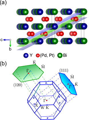
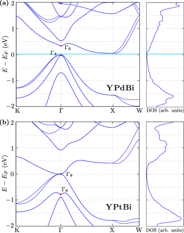
One of the most versatile systems that host numerous topological states of matter is the half-Heusler compounds [4, 23]. This family, with a simple MgAgAs-type cubic structure (space group ), that can be seen as a ZnS-type structure with filled octahedral lattice sites [Fig. 1 (a)] [23], has been extensively explored due to the fact that its semiconducting, magnetic, thermoelectric and strongly correlated properties can often be tailored [24, 25, 4, 26, 27, 28]. Earlier theoretical calculations have suggested that the mechanism behind the appearance of topological features in this family depends on the band inversion, which is very similar to the one observed in the prototypical CdTe and HgTe systems [29]. In both compounds, at the point near , the energy bands are split into , (both twofold degenerate) and (fourfold degenerate) states. This splitting originates from the zinc blende crystal symmetry and strong spin-orbit coupling [29, 30, 31, 32]. In the context of band topology, CdTe possesses a normal band order (the -like state sits above the -like state) while in HgTe band inversion occurs such that resides below [33]. Both situations are reproduced in YBi, where for = Pd the normal (trivial) state is realized, while for = Pt a band inversion occurs and non-trivial states emerge (see Fig. 9 in the Appendix) [29, 30, 31, 32].
In fact, previous angle resolved photoemission spectroscopy (ARPES) measurements on YPtBi have shown the presence of unusual topological surface states [34, 35]. Here, the topological surface states are observed throughout the Brillouin zone. This situation is different from the one typically observed, e.g., in the chalcogenides TIs, where the topological surface states emerge as a Dirac cone [36, 34, 33, 37]. Moreover, topological features were also observed in form of Weyl fermions in related half-Heusler semimetals PtBi ( = Nd, Gd, Yb) [38, 17, 39]. In particular, topological features can affect a possible superconducting state, even resulting in triplet superconductivity for some members of the Bi family ( = rare earth, = Pd or Pt) [40, 41, 42, 43, 44, 45, 46].
In an even more fundamental aspect, comparing YPtBi and YPdBi can be an excellent platform to experimentally tune the topological properties through the spin–orbit coupling. Both systems possess very similar lattice parameters [6.652(1) Å and 6.639(1) Å for YPtBi [41] and YPdBi [42], respectively], which makes the spin–orbit coupling the key parameter to distinguish between trivial (YPdBi) and non-trivial (YPtBi) topological states [30, 31, 32, 34, 35]. These compounds are particularly attractive due to the possibility of obtaining high quality thin films, increasing their potential applicability [47]. Previous nuclear magnetic resonance (NMR) [48, 49] and electron spin resonance (ESR) experiments [50] pointed toward a strong impact of spin–orbit coupling on the detailed band structure of YBi. A direct experimental visualization of the surface states resulting from band inversion in half-Heuslers has not been demonstrated, yet.
Additionally, although this family of materials supports so many different physical properties, which are often related to surface states, little is known about the surface properties of half-Heuslers. This is, at least in part, certainly related to the fact that half-Heusler compounds with cubic structure are notoriously difficult to cleave, rendering an in situ preparation of atomically flat surfaces from bulk samples a challenge. In consequence, reports employing scanning tunneling microscopy/spectroscopy (STM/STS) are scarce and focused on disordered surfaces in single crystals [51] or on the study of surface reconstructions in thin films [52]. In this work, we report on atomically flat surfaces investigated by STM/STS, combined with first-principles density functional theory (DFT) slab calculations, to explore the local properties of the half-Heuslers YPdBi and YPtBi. We cleaved our samples in situ, most likely along the (120) planes exposing a () reconstructed YBi-terminated surface. From our STS data we infer a finite local density of states (local DOS or LDOS) () at for YPtBi, while the trivial YPdBi compound exhibits a well defined gap around . We argue that the difference in the LDOS is likely due to the formation of metallic surface states in YPtBi, a finding corroborated by our slab calculations. Our work establishes the possibility of using STM as a local probe to investigate half-Heusler systems and suggests that a tuning of the LDOS can be achieved through the increase of the spin–orbit coupling upon going from Pd to Pt.
II Methods
Single crystalline samples of Y(Pd,Pt)Bi were synthesized by the Bi self flux growth technique with starting elements Y (99.99%):(Pd,Pt) (99.99%):Bi (99.999+%) in the proportion of 1:1:10 [53]. While YPtBi samples naturally expose (001), (110) and (111) planes in a pyramid-like shape, YPdBi samples only expose (001) planes (all samples had a cube-like shape). The investigated samples had an approximate size of 1 mm3.
STM/STS measurements were performed in a ultrahigh vacuum system at pressures Pa and at temperatures K. A total of seven (four YPdBi and three YPtBi) samples were cleaved in situ at temperatures K. The tunneling current was measured using electrochemical prepared tungsten tips and a bias voltage was applied to the samples. The topographies were obtained in a constant current mode with a predefined current set point . Most topographies were obtained in a dual-bias mode, i.e., forward and backward scans along the fast scan direction were obtained with a of the same magnitude, but with opposite signs. We did not see any differences in dual-bias mode (i.e. for the different values of ) when scanning the samples along the (120) planes. The d/d-spectra were acquired by a lock-in technique applying a modulation voltage of typically mV at Hz.
The first-principles density functional theory (DFT) calculations were performed using the projector augmented-wave (PAW) potentials [54] implemented in the Vienna Ab initio Simulation Package (vasp) code [55, 56, 57]. The calculations containing the spin–orbit coupling (SOC) were performed with the generalized gradient approximation (GGA) under the modified Becke-Johnson (mBJ) exchange potential [58, 59, 60]. The energy cutoff for the plane-wave expansion is set to eV. The density of states was calculated using k–point –centered grids in the Monkhorst–Pack scheme [61]. The lattice constants were assumed to be equal to the experimental values, i.e. Å for both compounds [62]. The band structures from the DFT calculations were used to find tight binding models by Wannier90 [63, 64], which allowed us to calculate surface state spectra by WannierTools [65]. The theoretical simulation of STM topographies for (120) YBi-terminated surfaces (without and with reconstruction) were computed using the Tersoff–Hamann approach [66]. Due to technical limitations of the mBJ potential for slab-type calculations, these specific DFT calculations were performed using a GGA with Perdew–Burke–Ernzerhof (PBE) parametrization [67]. More details on the calculations are provided in the Appendix D, Details of Bulk and surface band structure calculations.
III Results and Discussion
III.1 Topography of YPtBi single crystals
In situ preparation of clean surfaces (in case of bulk single crystals typically by cleaving) is of utmost importance for STM/STS studies but often exceedingly difficult for materials of cubic crystal structure [20]. Our single crystals of half-Heusler compounds YPdBi and YPtBi naturally expose (001) crystallographic planes, while the (111) plane was only found for YPtBi. Figure 1(b) shows the surface projection of the Brillouin zone along the latter direction. In principle, the pyramid-like shape of our YPtBi samples may open the possibility of exploring surfaces along the (001) and (111) planes. However, the YPdBi crystals had a more cube-like shape, suggesting a preferred cleave along the (001) plane. We emphasize that for a reasonable comparison between results obtained on both compounds it is vital to investigate identical crystallographic planes. Therefore, we focus on samples mounted along the (001) direction in the following (further details of measurements for cleaving YPtBi along the (111) plane are provided in Appendix A, see Figs. 4, 5 and 6).
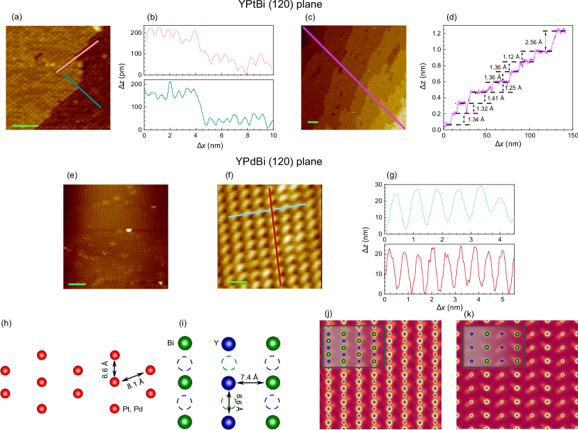
Atomically flat surfaces on cleaved half-Heuslers are extremely scarce and required extensive search. One example is shown in Fig. 2(a) for YPtBi where, in principle, the cleaving was expected to occur along the (001) plane. Before comparing the results from two different compounds, it is crucial to identify which planes and terminations are obtained since surface states depend decisively on those two parameters [34, 35]. Notably, all the obtained flat surfaces show a tilt angle with respect to the sample mounting plane (001) in this cleaving configuration. This is a hint that the obtained surfaces are not (001) planes. As will be argued below, the exposed planes are likely YBi-terminated (120) planes instead, which are highlighted in blue in Fig. 1(a).
Three crucial pieces of information are helpful to identify the cleaving plane: (i) As mentioned, the surfaces are tilted by with respect to the sample mounting plane. This renders the (120) plane a likely surface as it is expected 26.6∘ away from the (001) plane. (ii) The distance between corrugations and the (iii) the height of the step edges can be analyzed. Fig. 2(a) exemplifies the latter two in the same field of view. The apparent height profile as a function of the lateral distance (height scans) shown in Fig. 2(b) reveals a step edge height of pm and a distance between corrugations and nm for the pink and turquoise directions, respectively. Those distances are in agreement with the ones extracted from the Fourier transform of larger areas, from which we obtain and nm (see Fig. 7 in the Appendix).
In order to gain better statistics on the average step edge height a nm2 area obtained on YPtBi is investigated, Fig. 2(c). We can clearly see the occurrence of several step edges and a lack of adatoms. We note that the latter observation distinguishes the here observed surfaces over measurements on the (111) plane (compare Fig. 4 in the Appendix). The average step edge height between different exposed surfaces is pm [Fig. 2(d)] indicating that either exclusively YBi-terminated or Pt-terminated are observed. Note that the theoretically expected distance between these planes is 148 pm, see Fig. 1(a). A Pt-terminated surface can be ruled out since a distorted hexagonal lattice with distances between Pt atoms of 0.66 and 0.81 nm would be expected, Fig. 2(h), which is in clear contrast to the observation of Fig. 2(a). On the other hand, for a YBi-terminated surface a rectangular lattice with distances of 0.33 and 0.74 nm between atoms is expected. Therefore, we propose a () reconstructed YBi surface where half of the atoms are missing, see Fig. 2(i). This scenario is consistent with the observed distances between corrugations and STM simulations obtained through slab DFT calculations.
Reconstructed surfaces, including the type, are commonly observed on both, bulk samples [52] and thin films [68, 69, 70, 71] of half-Heusler compounds. The driving forces behind these reconstructions were argued to be charge neutrality and a minimization of the number of dangling bonds [52, 34, 35]. However, the (120) surface plane has not been investigated so far. In order to get further insight, we conducted first-principles slab calculations for this particular surface termination. Specifically, the total energies for slabs without and with reconstruction were calculated. The reconstructed slabs contained 84 sites, i.e. 28 atoms of each species (for further details see Appendix D). To allow comparison to the non-reconstructed surface, two Pd/Pt atoms were removed from one surface, but added as free atoms to the total energies. The calculations clearly favor a reconstructed surface by about 4.1 eV in case of YPdBi, and about 8.3 eV for YPtBi.
From the valence situation in the half-Heusler compounds, one may expect an YBi-terminated surface to be charge-neutral. In line with the statement above [52] one may then speculate about a minimum number of dangling bonds for the reconstructed surface and hence, a limited impact of dangling bonds on the surface properties.
III.2 Topography of YPdBi
Naturally, also on YPdBi atomically flat surfaces needed to be extensively searched for. Areas of nm2 could be identified, as exhibited in Fig. 2(e). However, we were not able to find any step edges in all of our investigated YPdBi cleaves. Importantly, within these areas we observed the same rectangular pattern as for YPtBi. This pattern is confirmed by high resolution topographies, as presented in Fig. 2(f), where the obtained distances between corrugations are and nm [Fig. 2(g)]. These values are consistent with results from Fourier analyses obtained on bigger areas (see Fig. 7 in the Appendix) as well as with the YPtBi results.
Apart from the missing step edges, all of the investigated, atomically flat areas on YPdBi appeared to be consistent with the plane orientation and termination as observed for YPtBi cleaves. In particular, the experimentally obtained surfaces are again tilted by with respect to the sample mounting plane (001). Hence, our observation point again toward reconstructed surfaces along the (120) plane.
Figures 2(j) and (k) represent STM simulations obtained through slab DFT calculations for YBi-terminated surfaces without and with reconstruction, respectively (for details, see Appendix D.3). These results indicate that without a surface reconstruction we would likely observe stripes along the (100) crystallographic direction [Fig. 2(j)]. Such stripes are absent on () reconstructed surfaces [Fig. 2(k)], in line with our observations.
The simulations also help explaining the subtle differences in the topographies upon going from Pd to Pt samples. For a (120) termination, the Pd/Pt atoms reside only 74 pm below the topmost YBi layer and hence, the Pd/Pt atoms may also contribute to the topography, as suggested by the yellow contributions in Figs. 2(j) and 2(k). The radial extent of the 4 orbitals is smaller than the 5 ones [72, 73]. Therefore, the second-to-topmost layer may have slightly different contributions to the topography depending on whether it is Pd or Pt.
III.3 Bulk properties of YBi ( Pd, Pt)
Before discussing our spectroscopic results of the surface properties of YPdBi and YPtBi, we address possible differences in the bulk DOS near for these two materials as this may easily influence the spectral weight measured at the surface.
As already mentioned, half-Heusler systems have a three dimensional character and, as such, bulk states might be relevant [74, 75]. In fact, previous specific heat studies have obtained very similar Sommerfeld coefficients for both systems. While for YPdBi mJ mol-1K-2 was reported [53], results for YPtBi ranged from 0.1 to mJ mol-1K-2 [76, 43]. Assuming a free conduction electron gas model with , where is the Bohr magneton and denotes the spin-resolved DOS at , one obtains eV-1 mol-1 spin-1 for YPdBi, and eV-1 mol-1 spin-1 for YPtBi. Such a negligible electronic contribution to the specific heat is consistent with previous transport measurements for both systems, which reported a semiconductor/semimetal-like behavior [41, 76, 53, 77, 43, 42, 44, 78].
It is worth noting that Pd/Pt and Bi-based compounds are known for hosting impurity phases, such as Bi and/or Pd/Pt-Bi binary phases [73]. Such impurity phases may affect the macroscopic properties, especially transport measurements. Consequently, it is highly desirable to have an experimental confirmation of the insulating bulk nature from a microscopic technique. Indeed, previous electron spin resonance measurements for rare-earth substituted YPdBi and YPtBi clearly indicate an insulating bulk behavior. This establishes the presence of a small gap in the bulk DOS at of both systems [76, 53], in agreement with our DFT results discussed below.
III.4 Spectroscopic results on YBi ( Pd, Pt)
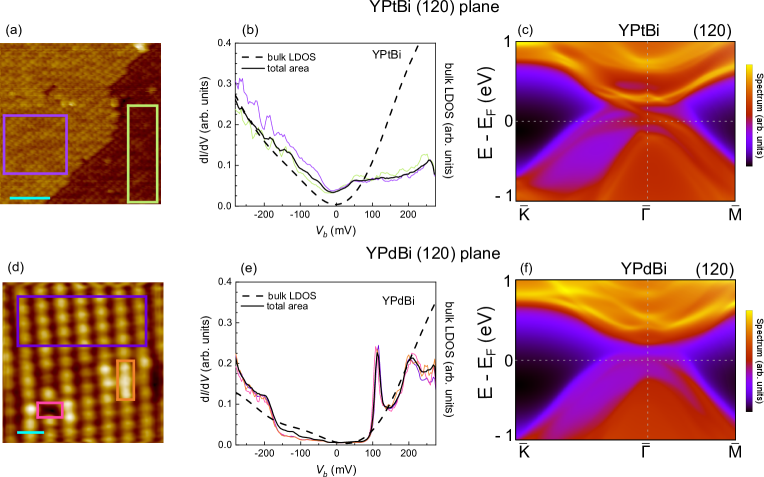
Having identified identical surface terminations and established negligible bulk contributions to the DOS near for both materials YPdBi and YPtBi, we can now compare their surface electronic properties. In Fig. 3(b) and (e) the STS results, i.e. d/d-spectra, are presented. We note that, within simplifying assumptions, d/d(). The topographic areas over which the spectroscopy curves were averaged are shown in Figs. 3(a) and (d), respectively, with the black curves in (b) and (e) obtained within the total areas of (a) and (d). Clearly, there are only minor differences between spectra obtained in different areas of a given compound. In particular, for YPdBi also spectra obtained at different defects are included, see orange and pink rectangles/curves in Fig. 3(d) and (e), which do not significantly deviate from the spectra in a clean (violet) or the total area. Consequently, the spectra are not significantly influenced by these defects.
The d/d-spectra of YPtBi are mostly featureless, with a -like shape near and a minimum at around meV. Most importantly, we obtain a finite LDOS around , which is a clear indication for a considerable amount of surface states closing the bulk gap.
This experimental result is to be contrasted with the bulk DOS as calculated by DFT [black dashed line in Fig. 3(b) and Appendix Fig. 9(b)], which predicts a gap-like behavior near . The calculations also find a mostly featureless spectrum and, for negative bias away from , qualitatively agree with our d/d-data. However, a proper analysis, and specifically insight into the details near , requires a slab calculation, the result of which is put forward in Fig. 3(c). The calculations were conducted with the Green function technique for semi-infinite systems assuming a (120) surface representing our experiments in a more realistic way. As discussed in the Appendix D.3, with the modified Becke-Johnson (mBJ) pseudopotential [58, 59, 60], it is neither possible to perform slab calculations using reconstructed surfaces nor to obtain the LDOS properly. Nonetheless, we are able to obtain important pieces of information to understand our STS results. As shown in Fig. 3(c), a mixture of surface states (non-trivial and trivial ones) contribute significantly to the spectral weight within the bulk gap, which is consistent with previous angle-resolved photoemission spectroscopy results [34, 35]. In other words, surface states dominate the LDOS near , which clearly indicates that the increase of the LDOS in YPtBi, compared to the bulk DOS, stems directly from those surface states. As shown in Fig. 3(c), near the point at 300 meV we obtain a high surface spectral weight of dangling bonds. Those trivial surface states are very similar to the van Hove singularity at approximately meV that is found for LuPtBi [31, 79, 80].
The results of our d/d-measurements for YPtBi become even more intriguing when compared to those of YPdBi, Fig. 3(e). There are two striking distinctions in the d/d-data of YPdBi: (i) Qualitatively, the LDOS exhibits more features, with a prominent peak at approximately 115 meV. (ii) Importantly, there is a clearly observable gap of width meV around . We should note, however, that the d/d-data for YPdBi do not strictly go all the way to zero, but remain finite at a very small value, possibly caused by thermal effects.
A comparison of the experimental data with the calculated bulk DOS is only partially possible, Fig. 3(e). On the one hand, the band gap eV [see Fig. 9(a) in the Appendix] in the projection to the (120) plane is comparable to the experimental value. This gap once again confirms the trivial nature of YPdBi, in which the conduction and valence bands are not inverted. Moreover, there appear to be no surface states near in this case. Most of the spectral weight coming from surface states is located above , which is consistent with our d/d being almost featureless at negative bias.
III.5 Comparison between YPtBi and YPdBi
The differences observed in the d/d-spectra of YPtBi and YPdBi are intriguing given the facts that identical surface terminations were investigated (thereby ruling out the surface reconstruction as the main cause of the differences) and both compound have very small bulk contributions to the DOS near . The slab calculated electronic band structures for the YBi-terminated (120) surface plane, Figs. 3(c) and (f), suggest a considerable admixture of non-trivial surface states to the DOS near in case of the YPtBi surface, which is absent for YPdBi. In such a case it is a likely scenario that the topological surface states are the key component for the differences in the d/d-spectra near . The minimum observed close to meV in case of YPtBi may then be linked to the Dirac point.
It is also interesting to note that the peak-like feature at meV is only observed for YPdBi. Two different origins could be at play to cause this peak. In the first scenario, which is suggested by our slab calculations, this feature coincides with the bottom of the conduction band, as shown in Fig. 3(f) and discussed in Appendix D.3 and Fig. 12. Here, the lack of this peak for YPtBi could naturally be explained by the band inversion in this compound. As discussed in the introduction, non-trivial surface states emerge thereupon.
An alternative scenario involves the presence of the surface reconstruction. Here, the peak would be a direct consequence of the enhancement of trivial surface states. However, in this scenario one should also expect such a peak for YPtBi, which is not observed experimentally. We emphasize that such a comparison is only possible since results obtained on identical surface terminations (concerning the type and arrangement of the surface atoms as well as the orientation of the terminating plane) are compared. The clear difference between the LDOS of both systems near favours the increased spin–orbit coupling (upon going from Pd to Pt) as the source of the appearance of surface states with topological character. The predicted, strong modification of these surface states has, to the best of our knowledge, not been demonstrated by STM/S before and suggests a systematic tunability of topology in half-Heusler systems. Likely, by choosing the proper surface plane, these properties also may be accessed through macroscopic (e.g. transport) measurements.
Finally, our results, even though obtained at K, may also shed some light on superconductivity in half-Heusler systems. A well defined gap was found for the trivial insulator YPdBi. This compound has been reported to have one of the highest superconducting transition temperatures ( K) among the PdBi family [44]. If the superconductivity is intrinsic, it would be interesting to understand how a gapped system can develop a superconducting phase. In this respect it is interesting to note that, at least for YPtBi, some reports discuss the possibility of superconductivity being a bulk or a surface property [41, 47]. Yet, a finite LDOS, possibly with Dirac point(s), for YPtBi is not inconsistent with a topological superconductivity scenario [40, 41, 42, 43, 45, 46, 47, 81]. It would be interesting to conduct further experiments at mK temperatures to investigate the origin of superconductivity and its nature in half-Heusler systems.
IV Conclusion
In summary, we performed scanning tunneling microscopy/spectroscopy on the half-Heusler systems YPtBi and YPdBi. By in situ cleaving the single crystals at low temperatures we were able to investigate atomically flat areas. Both materials very likely expose (120) YBi-terminated surfaces with () reconstructions which induce additional surface states and hence, may complicate surface spectroscopy. Using STM, we can compare identical surface terminations, thereby ruling out the reconstructions as the main cause for differences in the spectroscopic results between the two materials. However, we do observe a clear difference in the LDOS of these compounds: While YPdBi exhibits a gap of 100 meV around , surface states are found for YPtBi without indication of a gap. Such distinct behavior was not seen by macroscopic measurements reported in previous studies. Our result provides evidence for the targeted realization of unusual surface states. DFT calculations are consistent with such change in the LDOS.
In a more general way, our result can very likely be linked to a spin–orbit tuning of topology in half-Heusler systems. More importantly, our results emphasize the key role of surface states near in these systems. Exploring planes such as the (120) surface termination [or even the (001) plane in thin films] appears as an extremely promising route to obtain a versatile TI with an insulating bulk and increases the potential of half-Heusler systems for applications.
Acknowledgments
We thank E. H. da Silva Neto, T. J. Boyle and M. Walker for their help and discussions in the beginning of this project. This work was supported by FAPESP (SP-Brazil) Grants No 2020/12283-0, 2018/11364-7, 2017/10581-1, CNPq grant No 311783/2021-0 and CAPES. Work was also supported by the National Science Centre (NCN, Poland) under Projects No. 2021/43/B/ST3/02166 (A.P.). A.P. appreciates funding within the frame of scholarships of the Minister of Science and Higher Education of Poland for outstanding young scientists (2019 edition, No. 818/STYP/14/2019). Work at Los Alamos was supported by the Los Alamos Laboratory Directed Research and Development program through project 20210064DR.
Appendix A (111) plane in YPtBi
A.1 STM/STS results
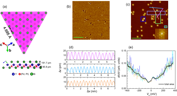
In YPtBi crystals with pyramid-like shape we are also able to cleave along the (111) plane; the results are summarized in Fig. 4. In this plane, the height difference between Y and Bi layers is twice as large as the Y-Pt or Pt-Bi layer spacing, see Fig. 4(a). Furthermore, fewer chemical bonds need to be broken between Y and Bi layers compared to cleaves involving Pt layers, which should result in cleaves exposing mostly Y or Bi layers [34]. We found more easily atomically flat surfaces along the (111) plane when compared to the cleaves along the (120) plane for YPtBi. Yet, atomically flat surfaces needed to be
extensively searched for, which is not surprising in a cubic system. Importantly, however, despite great efforts atomically flat areas on a (111) plane could not be found on YPdBi and therefore, the comparison of the LDOS for both compounds was focused on the (120) plane.
The cleave along the (111) plane should expose either Y- or Bi-terminated triangular lattices, as shown in Fig. 4(a). Fig. 4(b) exhibits a nm2 topography. Albeit we were able to locate such large atomically flat areas, there was quite an amount of adatoms on top of such surfaces. The topography in Fig. 4(c) zooms into an area of nm2. In this case it is possible to observe in more detail the triangular lattice, which is confirmed by the Fourier transform presented in the lower right inset. Again, we obtain a moderate amount of adatoms, which are expected on an unreconstructed surface due to its polar nature. The establishment of an unreconstructed surface is further corroborated by the distance
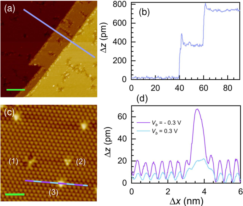
between corrugations, as highlighted in the height scans of Fig. 4(d). We obtain a distance between corrugations of nm, nm, and nm for the magenta, blue and orange lines, respectively, which is in excellent agreement with the theoretical distance between Bi/Y atoms of nm along the (111) plane. As we will discuss in more detail below, the exposed surface is likely an unreconstructed Bi-terminated surface.
In Fig. 4(e) we present d/d-spectra, which were obtained within in
the total field of view of Fig. 4(c) (black line) as well as within the areas marked by colored rectangles (with the colors corresponding to those of the spectra). Earlier theoretical calculations indicated a Dirac point buried in the bulk DOS for either Y- or Bi-terminated surfaces, which was confirmed by angle resolved photoemission spectroscopy [34, 35]. Nonetheless, trivial Rashba-like surface states can be expected due to the presence of dangling bonds [34, 52]. The observed d/d-spectra are almost featureless, with a finite DOS at the Fermi level . Interestingly, the LDOS obtained at two adatoms [yellow area in Fig. 4(c)], or at defects [blue area in Fig. 4(c)] does not change significantly when compared to the LDOS obtained on clean surfaces (green and purple areas and spectra) or even to the spectrum averaged over the total field of view. This is an indication that the surface states are not affected locally by small amounts of disorder.
In order to provide further evidence to the (111) assignment of the terminating plane observed in Fig. 4, we experimentally explored the presence of step edges and adatoms. Fig. 5(a) shows a typical 100 x 100 nm2 topography along the (111) plane with two step edges. As can be seen in Fig. 5(b), the height difference between each exposed surface is pm. Such a distance is consistent to either Y–Y, Bi–Bi or Pd–Pd/Pt–Pt surface terminations for which pm is expected. It is worth to note that there is an accumulation of adatoms along the edges of the exposed surfaces (small peaks in the height scan), which reinforces our assumption above that such adatoms play a role in neutralization of the exposed polar surfaces.
Such an assumption is also corroborated by different apparent heights of the adatom if measured with different bias . Fig. 5(c) shows a nm2 topography taken with mV. We can observe the three most numerous defects obtained on these surfaces: a triangular one likely related to a vacancy [defect (1)], a small triangle which could be related to a substitution in a sub-layer underneath the exposed surface [defect (2)] and the already mentioned adatoms [defect (3)]. Fig. 5(d) provides the height scan across the adatom position in Fig. 5(c) with different values of the applied obtained in dual-bias mode (i.e. at exactly the same position). We systematically observe higher heights at the adatom sites for negative . For negative (positive) , the tip will have a positive (negative) potential with respect to the sample. In this scenario, the tip gets further away from (closer to) the adatom if it has a more positive charge compared to the surrounding bulk. We expect a valence of for Y, while the other constituents in YPtBi should have a more negative valence. Consequently, an adatom is much more likely more positive as its surrounding on a Bi or Pt terminated surface. Since a cleave exposing Pt is unlikely from the chemical bonding situation discussed above, we speculate that we obtained a Bi terminated surface in Fig. 5.
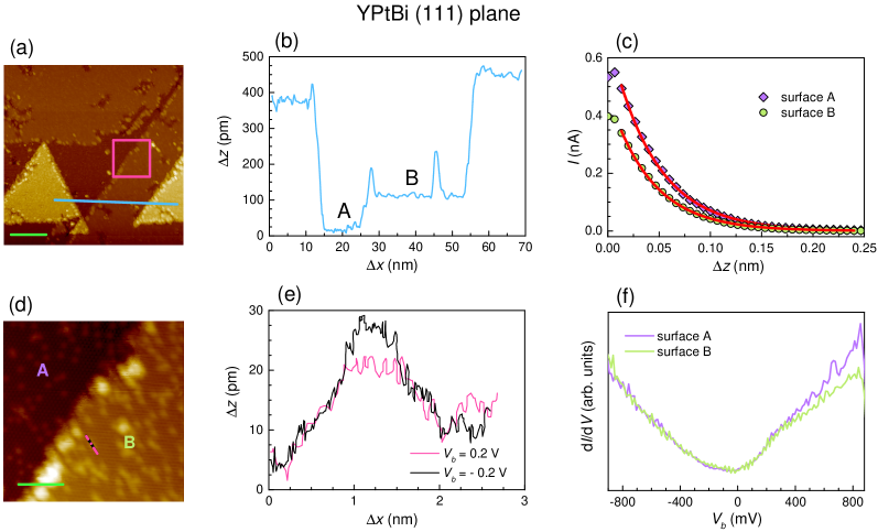
A.2 Coexistence of Pt and Bi-terminated surfaces
As already pointed out, the majority of the YPtBi samples which successfully cleaved along the (111) plane exposed the same termination within the field of view (even when step edges were included, cf. Fig. 5). However, in one particular field of view we were able to observe a coexistence of two differently terminated surfaces. Fig. 6(a) shows this nm2 topography. In the height scan explored in Fig. 6(b) we obtain a step height between two consecutive surfaces (labeled and ) of pm. This value is much smaller than the expected step height = 383 pm for identical terminations. Indeed, it is close to the Pt–Bi (or Pt–Y) layer distance, which is pm [Fig. 4(a)]. Such a step height necessarily implies that one of the surfaces has to have a Pt termination.
The difference between those two surface terminations is also manifested by two different heights of the tunneling barrier , which is closely related to the work function of the sample (note that also the tip work function enters into ). can be obtained from an analysis of as a function of the tip-sample distance . For clean surfaces, with , where is the bare electron mass and . Fig. 6(c) represents curves for surfaces and , which are identified in Figs. 6(b) and (d). By fitting the curves, red lines in Fig. 6(c), we obtain eV and eV. A fair comparison here is to look at the values of the elemental materials. For Y, Bi and Pt, eV, eV, and eV, respectively. Comparing to our obtained results, one may speculate that the highest obtained value, i.e. , is unlikely from an Y-terminated surface and, conversely, the lower value does not stem from a Pt-terminated surface. As one of the two surfaces ( or ) has to be Pt-terminated, it is likely surface .
A closer look at height scans across defects can also be informative with respect to the assignment of those two distinct surfaces. A zoom into the magenta box of Fig. 6(a) is given in Fig. 6(d). According to Fig. 6(b), we identify the differently terminated surfaces as and in the nm2 topography. The height scans across a defect at surface for opposite signs are shown in Fig. 6(e). They were taken at the positions highlighted by the magenta and black lines in Fig. 6(d). It is straightforward to note that the difference of the defect height for opposite -values is much smaller on this surface when compared to the adatom height at surface (which was assigned as Bi-terminated), cf. Fig. 5(d). In consequence, the defect investigated in Fig. 6(e) is very likely located in a sub-surface layer, i.e., in a layer underneath the exposed surface.
Finally, Fig. 6(f) represents d/d-spectra as a function of for both surfaces. Surprisingly, there is only a small difference at higher positive -values between the spectra of the two differently terminated surfaces, suggesting that the LDOS is dominated by bulk and trivial surfaces state contributions in both cases.
Appendix B Fourier transform of the planes
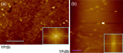
A more accurate extraction of the distance between corrugations can be achieved by analyzing the Fourier transform of larger areas. In the case of YPtBi, one large flat area that we were able to obtain is shown in Fig. 7(a). From the Fourier transform (inset), we obtained = 0.67(3) and 0.70(3) nm. For YPdBi, a large, atomically flat area is presented in Fig. 7(b). Here, the Fourier transform yielded = 0.61(3) and 0.72(3) nm. It is worth to notice that the Fourier transforms even have a slightly rectangular shape [see also Fig. 2(i)], consistent with the asymmetry between the distance of corrugations.
Appendix C Reproducibility of the spectra
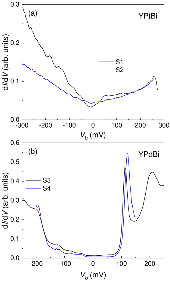
As mentioned in Sec. II, four YPdBi and three YPtBi samples were cleaved in situ and subsequently investigated by STM/STS. In order to provide support for the reproducibility of our data, specifically the spectra, we here exemplify results obtained on different samples of YPtBi as well as YPdBi. For comparison, we also reproduced in Fig. 8 the spectra of Fig. 3, marked S1 and S3, respectively. Clearly, the spectra of different samples of a given material compare well, and all the main features are reproduced. Most important for the main conclusion of our investigation, the reduction of the LDOS at is clearly reproduced upon going from YPtBi to YPdBi.
Appendix D Details of Bulk and surface band structure calculations
D.1 Bulk band structure calculations
We were able to reproduce the bands at point using the modified Becke-Johnson (mBJ) pseudopotential, see Fig. 9, as given in [30, 29]. Here, the topological properties can be described by , which is negative for systems with band inversion [29] (as mentioned in the introduction). Indeed, for YPdBi we find eV, while for YPtBi we obtain approximately eV. In other words, our calculations specify YPtBi as a zero-gap semiconductor. Both values are similar to those reported earlier [29, 31, 30]. It is worth to point out that even though different pseudopotentials might result in similar densities of states, some of those pseudopotentials do not reproduce correctly the band inversion [82]. Finally, these results depend strongly on the lattice constant [31].
D.2 Slab calculations for the (111) plane
The surface spectral functions, calculated within the Green function technique for semi-infinite systems, for the (111) surface planes of YPdBi and YPtBi are presented
in Figs. 10(a) and (b), respectively [cf. Figs. 3(c) and (f) for
the (120) plane]. In the case of a Bi-terminated (111) surface of YPdBi, there is no
Dirac point at the point, as expected [Fig. 10(a)]. In the
YPtBi case, the Dirac point appears below the Fermi level , as seen
in Fig. 10(b). This result is consistent with previous DFT calculations and
ARPES experiments [34, 35]. It is worth to note
that our slab calculations improve our understanding of the lack of changes in the LDOS
near defects in this plane, cf. Fig. 4(e). As discussed in Sec. III.4, the bulk LDOS has some impact in our data. Near , we
find trivial and topological bands, which may complicate the scattering process even
further. Therefore, the change in the LDOS due to trivial surface states may be hard
to detect within this energy window.
D.3 Direct slab band structure calculations
Due to the technical limitations of the mBJ potential implemented in vasp, it cannot be used directly to study the slab band structure. As such, to present the main impact of the surface reconstruction on the electronic band structure, we performed DFT calculations using GGA with Perdew–Burke–Enzerhof (PBE) parametrization [67]. Here, we should emphasize that this approach (DFT with GGA + PBE) does not correctly reproduce the bulk band structure of half-Heusler compounds, a problem well reported in the literature [58, 59, 60]. This is reflected in the absence of the band gap for YPdBi [cf. Fig. 9(a) and Fig. 11(a)] or incorrect band curvatures around the point in the band structure of YPtBi [cf. Fig. 9(b) and Fig. 11(b)]. Nevertheless, this type of calculation can be used to present the main features of the band structure of (120) surfaces with reconstruction.
without reconstruction with reconstruction
 YPtBi YPdBi
For the simulation of the (120) surface band structure, we constructed slab models containing 3 layers of the discussed compounds (mostly 28 formula units). The reconstructions of the surface was introduced ’’by hand‘‘, i.e., by removing some atoms from the surfaces. From the self-consistently found charge distributions, the STM simulations were computed [see Figs. 2(j) and (k)]. Similarly, the electronic band structure for both compounds are presented in Fig. 12 where the results obtained for surfaces without and with surface reconstruction are presented on the left and right panels, respectively. For both YPdBi and YPtBi (120) surfaces without reconstruction (left panels in Fig. 12), we observed the realization of the surface states above . The introduction of surface reconstructions on the (120) surface led to a multiplication of the surface states, an effect that is well visible at the M points in the right panels of Fig. 12. The additional, ’’extra‘‘ surface states come from the hanging (non-bonded) orbitals in the surface plane, due to the absence of some atoms on the surface (i.e. the surface reconstruction). This main feature of the band structure for the reconstructed surface, i.e. the surface states multiplication, is expected to also be present in case of a ’’correctly‘‘ obtained band structure, i.e. if calculated with mBJ potential.
References
- von Klitzing et al. [1980] K. von Klitzing, G. Dorda, and M. Pepper, New method for high-accuracy determination of the fine-structure constant based on quantized Hall resistance, Phys. Rev. Lett. 45, 494 (1980).
- Bernevig et al. [2006] B. A. Bernevig, T. L. Hughes, and S.-C. Zhang, Quantum spin Hall effect and topological phase transition in HgTe quantum wells, Science 314, 1757 (2006).
- König et al. [2007] M. König, S. Wiedmann, C. Brüne, A. Roth, H. Buhmann, L. W. Molenkamp, X.-L. Qi, and S.-C. Zhang, Quantum spin Hall insulator state in HgTe quantum wells, Science 318, 766 (2007).
- Manna et al. [2018] K. Manna, Y. Sun, L. Muechler, J. Kübler, and C. Felser, Heusler, Weyl and Berry, Nat. Rev. Mater. 3, 244 (2018).
- Armitage et al. [2018] N. P. Armitage, E. J. Mele, and A. Vishwanath, Weyl and Dirac semimetals in three-dimensional solids, Rev. Mod. Phys. 90, 015001 (2018).
- Hasan and Kane [2010] M. Z. Hasan and C. L. Kane, Colloquium: topological insulators, Rev. Mod. Phys. 82, 3045 (2010).
- Lv et al. [2021] B. Q. Lv, T. Qian, and H. Ding, Experimental perspective on three-dimensional topological semimetals, Rev. Mod. Phys. 93, 025002 (2021).
- Wang et al. [2016] Z. Wang, A. Alexandradinata, R. J. Cava, and B. A. Bernevig, Hourglass fermions, Nature 532, 189 (2016).
- Xu et al. [2012] S.-Y. Xu, M. Neupane, C. Liu, D. Zhang, A. Richardella, L. A. Wray, N. Alidoust, M. Leandersson, T. Balasubramanian, J. Sánchez-Barriga, et al., Hedgehog spin texture and Berry phase tuning in a magnetic topological insulator, Nat. Phys. 8, 616 (2012).
- Tokura et al. [2017] Y. Tokura, M. Kawasaki, and N. Nagaosa, Emergent functions of quantum materials, Nat. Phys. 13, 1056 (2017).
- Singh et al. [2022] B. Singh, H. Lin, and A. Bansil, Topology and Symmetry in Quantum Materials, Adv. Mater. 35, 2201058 (2022).
- Singh et al. [2016] B. Singh, H. Lin, R. Prasad, and A. Bansil, Role of surface termination in realizing well-isolated topological surface states within the bulk band gap in TlBiSe2 and TlBiTe2, Phys. Rev. B 93, 085113 (2016).
- Eguchi et al. [2015] G. Eguchi, K. Kuroda, K. Shirai, Y. Ando, T. Shinjo, A. Kimura, and M. Shiraishi, Precise determination of two-carrier transport properties in the topological insulator TlBiSe2, Phys. Rev. B 91, 235117 (2015).
- Eremeev et al. [2012] S. V. Eremeev, G. Landolt, T. V. Menshchikova, B. Slomski, Y. M. Koroteev, Z. S. Aliev, M. B. Babanly, J. Henk, A. Ernst, L. Patthey, et al., Atom-specific spin mapping and buried topological states in a homologous series of topological insulators, Nat. Commun. 3, 635 (2012).
- Jiao et al. [2018] L. Jiao, S. Rößler, D. Kasinathan, P. F. S. Rosa, C. Guo, H. Q. Yuan, C.-X. Liu, Z. Fisk, F. Steglich, and S. Wirth, Magnetic and defect probes of the SmB6 surface state, Sci. Adv. 4, eaau4886 (2018).
- Pirie et al. [2020] H. Pirie, Y. Liu, A. Soumyanarayanan, P. Chen, Y. He, M. M. Yee, P. F. S. Rosa, J. D. Thompson, D.-J. Kim, Z. Fisk, X. Wang, J. Paglione, D. K. Morr, M. H. Hamidian, and J. E. Hoffman, Imaging emergent heavy Dirac fermions of a topological Kondo insulator, Nat. Phys. 16, 52 (2020).
- Guo et al. [2018] C. Guo, F. Wu, Z. Wu, M. Smidman, C. Cao, A. Bostwick, C. Jozwiak, E. Rotenberg, Y. Liu, F. Steglich, et al., Evidence for Weyl fermions in a canonical heavy-fermion semimetal YbPtBi, Nat. Commun. 9, 4622 (2018).
- Dzsaber et al. [2021] S. Dzsaber, X. Yan, M. Taupin, G. Eguchi, A. Prokofiev, T. Shiroka, P. Blaha, O. Rubel, S. E. Grefe, H.-H. Lai, et al., Giant spontaneous Hall effect in a nonmagnetic Weyl-Kondo semimetal, Proc. Natl. Acad. Sci. U.S.A. 118, e2013386118 (2021).
- Aishwarya et al. [2022] A. Aishwarya, Z. Cai, A. Raghavan, M. Romanelli, X. Wang, X. Li, G. Gu, M. Hirsbrunner, T. Hughes, F. Liu, et al., Spin-selective tunneling from nanowires of the candidate topological Kondo insulator SmB6, Science 377, 1218 (2022).
- Wirth and Schlottmann [2021] S. Wirth and P. Schlottmann, An STM perspective on hexaborides: Surface states of the Kondo insulator SmB6, Adv. Quantum Technol. 4, 2100102 (2021).
- Paschen and Si [2021] S. Paschen and Q. Si, Quantum phases driven by strong correlations, Nat. Rev. Phys. 3, 9 (2021).
- Palmstrøm [2003] C. Palmstrøm, Epitaxial Heusler alloys: New materials for semiconductor spintronics, MRS bulletin 28, 725 (2003).
- Graf et al. [2011] T. Graf, C. Felser, and S. S. P. Parkin, Simple rules for the understanding of Heusler compounds, Prog. Solid State Chem. 39, 1 (2011).
- Zeier et al. [2016] W. G. Zeier, J. Schmitt, G. Hautier, U. Aydemir, Z. M. Gibbs, C. Felser, and G. J. Snyder, Engineering half-Heusler thermoelectric materials using Zintl chemistry, Nat. Rev. Mater. 1, 16032 (2016).
- Mun et al. [2013] E. D. Mun, S. L. Bud‘ko, C. Martin, H. Kim, M. A. Tanatar, J.-H. Park, T. Murphy, G. M. Schmiedeshoff, N. Dilley, R. Prozorov, and P. C. Canfield, Magnetic-field-tuned quantum criticality of the heavy-fermion system YbPtBi, Phys. Rev. B 87, 075120 (2013).
- Hundley et al. [1997] M. F. Hundley, J. D. Thompson, P. C. Canfield, and Z. Fisk, Electronic transport properties of the semimetallic heavy fermion YbBiPt, Phys. Rev. B 56, 8098 (1997).
- Fisk et al. [1991] Z. Fisk, P. C. Canfield, W. P. Beyermann, J. D. Thompson, M. F. Hundley, H. R. Ott, E. Felder, M. B. Maple, M. A. Lopez de la Torre, P. Visani, and C. L. Seaman, Massive electron state in YbBiPt, Phys. Rev. Lett. 67, 3310 (1991).
- Eriksson et al. [1992] O. Eriksson, J. Wills, and A. Boring, Electronic structure of the RBiPt compounds (R = Y and Yb), J. Alloys Compd. 185, 145 (1992).
- Feng et al. [2010] W. Feng, D. Xiao, Y. Zhang, and Y. Yao, Half-Heusler topological insulators: A first-principles study with the Tran-Blaha modified Becke-Johnson density functional, Phys. Rev. B 82, 235121 (2010).
- Al-Sawai et al. [2010] W. Al-Sawai, H. Lin, R. S. Markiewicz, L. A. Wray, Y. Xia, S.-Y. Xu, M. Z. Hasan, and A. Bansil, Topological electronic structure in half-Heusler topological insulators, Phys. Rev. B 82, 125208 (2010).
- Chadov et al. [2010] S. Chadov, X. Qi, J. Kübler, G. H. Fecher, C. Felser, and S. C. Zhang, Tunable multifunctional topological insulators in ternary Heusler compounds, Nat. Mater. 9, 541 (2010).
- Lin et al. [2010] H. Lin, L. A. Wray, Y. Xia, S. Xu, S. Jia, R. J. Cava, A. Bansil, and M. Z. Hasan, Half-Heusler ternary compounds as new multifunctional experimental platforms for topological quantum phenomena, Nat. Mater. 9, 546 (2010).
- Zhu et al. [2012] Z. Zhu, Y. Cheng, and U. Schwingenschlögl, Band inversion mechanism in topological insulators: A guideline for materials design, Phy. Rev. B 85, 235401 (2012).
- Liu et al. [2016] Z. Liu, L. Yang, S.-C. Wu, C. Shekhar, J. Jiang, H. Yang, Y. Zhang, S.-K. Mo, Z. Hussain, B. Yan, et al., Observation of unusual topological surface states in half-Heusler compounds LnPtBi (Ln= Lu, Y), Nat. Commun. 7, 12924 (2016).
- Hosen et al. [2020] M. M. Hosen, G. Dhakal, K. Dimitri, H. Choi, F. Kabir, C. Sims, O. Pavlosiuk, P. Wiśniewski, T. Durakiewicz, J.-X. Zhu, D. Kaczorowski, and M. Neupane, Observation of Dirac state in half-Heusler material YPtBi, Sci. Rep. 10, 12343 (2020).
- King et al. [2011] P. D. C. King, R. C. Hatch, M. Bianchi, R. Ovsyannikov, C. Lupulescu, G. Landolt, B. Slomski, J. H. Dil, D. Guan, J. L. Mi, E. D. L. Rienks, J. Fink, A. Lindblad, S. Svensson, S. Bao, G. Balakrishnan, B. B. Iversen, J. Osterwalder, W. Eberhardt, F. Baumberger, and P. Hofmann, Large tunable Rashba spin splitting of a two-dimensional electron gas in Bi2Se3, Phys. Rev. Lett. 107, 096802 (2011).
- Ruan et al. [2016] J. Ruan, S.-K. Jian, H. Yao, H. Zhang, S.-C. Zhang, and D. Xing, Symmetry-protected ideal Weyl semimetal in HgTe-class materials, Nat. Commun. 7, 11136 (2016).
- Hirschberger et al. [2016] M. Hirschberger, S. Kushwaha, Z. Wang, Q. Gibson, S. Liang, C. A. Belvin, B. A. Bernevig, R. J. Cava, and N. P. Ong, The chiral anomaly and thermopower of Weyl fermions in the half-Heusler GdPtBi, Nat. Mater. 15, 1161 (2016).
- Shekhar et al. [2018] C. Shekhar, N. Kumar, V. Grinenko, S. Singh, R. Sarkar, H. Luetkens, S.-C. Wu, Y. Zhang, A. C. Komarek, E. Kampert, et al., Anomalous Hall effect in Weyl semimetal half-Heusler compounds RPtBi (R = Gd and Nd), Proc. Natl. Acad. Sci. U.S.A. 115, 9140 (2018).
- Brydon et al. [2016] P. M. R. Brydon, L. Wang, M. Weinert, and D. F. Agterberg, Pairing of j = 3/2 fermions in half-Heusler superconductors, Phys. Rev. Lett. 116, 177001 (2016).
- Butch et al. [2011] N. P. Butch, P. Syers, K. Kirshenbaum, A. P. Hope, and J. Paglione, Superconductivity in the topological semimetal YPtBi, Phys. Rev. B 84, 220504(R) (2011).
- Gofryk et al. [2011] K. Gofryk, D. Kaczorowski, T. Plackowski, A. Leithe-Jasper, and Y. Grin, Magnetic and transport properties of rare-earth-based half-Heusler phases RPdBi: Prospective systems for topological quantum phenomena, Phys. Rev. B 84, 035208 (2011).
- Pavlosiuk et al. [2016] O. Pavlosiuk, D. Kaczorowski, and P. Wiśniewski, Superconductivity and Shubnikov-de Haas oscillations in the noncentrosymmetric half-Heusler compound YPtBi, Phys. Rev. B 94, 035130 (2016).
- Nakajima et al. [2015] Y. Nakajima, R. Hu, K. Kirshenbaum, A. Hughes, P. Syers, X. Wang, K. Wang, R. Wang, S. R. Saha, D. Pratt, et al., Topological RPdBi half-Heusler semimetals: A new family of noncentrosymmetric magnetic superconductors, Sci. Adv. 1, e1500242 (2015).
- Kim et al. [2021] H. Kim, M. A. Tanatar, H. Hodovanets, K. Wang, J. Paglione, and R. Prozorov, Campbell penetration depth in low carrier density superconductor YPtBi, Phys. Rev. B 104, 014510 (2021).
- Kim et al. [2018] H. Kim, K. Wang, Y. Nakajima, R. Hu, S. Ziemak, P. Syers, L. Wang, H. Hodovanets, J. D. Denlinger, P. M. Brydon, et al., Beyond triplet: Unconventional superconductivity in a spin-3/2 topological semimetal, Sci. Adv. 4, eaao4513 (2018).
- Kim et al. [2023] J. Kim, K. M. Fijalkowski, J. Kleinlein, C. Schumacher, A. Markou, C. Gould, S. Schreyeck, C. Felser, and L. W. Molenkamp, Molecular beam epitaxy of a half-Heusler topological superconductor candidate YPtBi, Phys. Rev. Mater. 7, 024802 (2023).
- Nowak and Kaczorowski [2014] B. Nowak and D. Kaczorowski, NMR as a probe of band inversion in topologically nontrivial half-Heusler compounds, J. Phys. Chem. C 118, 18021 (2014).
- Zhang et al. [2016] X. Zhang, Z. Hou, Y. Wang, G. Xu, C. Shi, E. Liu, X. Xi, W. Wang, G. Wu, and X.-x. Zhang, NMR evidence for the topologically nontrivial nature in a family of half-Heusler compounds, Sci. Rep. 6, 23172 (2016).
- Lesseux et al. [2016] G. G. Lesseux, T. M. Garitezi, P. F. S. Rosa, C. B. R. Jesus, S. B. Oseroff, J. L. Sarrao, Z. Fisk, R. R. Urbano, P. G. Pagliuso, and C. Rettori, Unusual diffusive effects on the ESR of Nd3+ ions in the tunable topologically nontrivial semimetal YBiPt, J. Phys.: Condens. Matter 28, 125601 (2016).
- Baek et al. [2015] H. Baek, J. Ha, D. Zhang, B. Natarajan, J. P. Winterstein, R. Sharma, R. Hu, K. Wang, S. Ziemak, J. Paglione, et al., Creating nanostructured superconductors on demand by local current annealing, Phys. Rev. B 92, 094510 (2015).
- Kawasaki et al. [2018] J. K. Kawasaki, A. Sharan, L. I. Johansson, M. Hjort, R. Timm, B. Thiagarajan, B. D. Schultz, A. Mikkelsen, A. Janotti, and C. J. Palmstrøm, A simple electron counting model for half-Heusler surfaces, Sci. Adv. 4, eaar5832 (2018).
- Souza et al. [2019] J. C. Souza, C. B. R. Jesus, G. G. Lesseux, P. F. S. Rosa, R. R. Urbano, and P. Pagliuso, Crystalline electric field study in a putative topologically trivial rare-earth doped YPdBi compound, J. Phys. Condens. Matter 31, 465701 (2019).
- Blöchl [1994] P. E. Blöchl, Projector augmented-wave method, Phys. Rev. B 50, 17953 (1994).
- Kresse and Hafner [1994] G. Kresse and J. Hafner, Ab initio molecular-dynamics simulation of the liquid-metal–amorphous-semiconductor transition in germanium, Phys. Rev. B 49, 14251 (1994).
- Kresse and Furthmüller [1996] G. Kresse and J. Furthmüller, Efficient iterative schemes for ab initio total-energy calculations using a plane-wave basis set, Phys. Rev. B 54, 11169 (1996).
- Kresse and Joubert [1999] G. Kresse and D. Joubert, From ultrasoft pseudopotentials to the projector augmented-wave method, Phys. Rev. B 59, 1758 (1999).
- Becke and Johnson [2006] A. D. Becke and E. R. Johnson, A simple effective potential for exchange, J. Chem. Phys. 124, 221101 (2006).
- Tran and Blaha [2009] F. Tran and P. Blaha, Accurate band gaps of semiconductors and insulators with a semilocal exchange-correlation potential, Phys. Rev. Lett. 102, 226401 (2009).
- Camargo-Martínez and Baquero [2012] J. A. Camargo-Martínez and R. Baquero, Performance of the modified Becke-Johnson potential for semiconductors, Phys. Rev. B 86, 195106 (2012).
- Monkhorst and Pack [1976] H. J. Monkhorst and J. D. Pack, Special points for Brillouin-zone integrations, Phys. Rev. B 13, 5188 (1976).
- Haase et al. [2002] M. G. Haase, T. Schmidt, C. G. Richter, H. Block, and W. Jeitschko, Equiatomic rare earth (Ln) transition metal antimonides LnSb (Rh, Lr) and bismuthides LnBi (Rh, Ni, Pd, Pt), J. Solid State Chem. 168, 18 (2002).
- Mostofi et al. [2014] A. A. Mostofi, J. R. Yates, G. Pizzi, Y.-S. Lee, I. Souza, D. Vanderbilt, and N. Marzari, An updated version of wannier90: A tool for obtaining maximally-localised Wannier functions, Comput. Phys. Commun. 185, 2309 (2014).
- Pizzi et al. [2020] G. Pizzi, V. Vitale, R. Arita, S. Blügel, F. Freimuth, G. Géranton, M. Gibertini, D. Gresch, C. Johnson, T. Koretsune, J. Ibañez-Azpiroz, H. Lee, J.-M. Lihm, D. Marchand, A. Marrazzo, Y. Mokrousov, J. I. Mustafa, Y. Nohara, Y. Nomura, L. Paulatto, S. Poncé, T. Ponweiser, J. Qiao, F. Thöle, S. S. Tsirkin, M. Wierzbowska, N. Marzari, D. Vanderbilt, I. Souza, A. A. Mostofi, and J. R. Yates, Wannier90 as a community code: new features and applications, J. Phys.: Condens. Matter 32, 165902 (2020).
- Wu et al. [2018] Q. S. Wu, S. N. Zhang, H.-F. Song, M. Troyer, and A. A. Soluyanov, WannierTools: An open-source software package for novel topological materials, Comput. Phys. Commun. 224, 405 (2018).
- Tersoff and Hamann [1985] J. Tersoff and D. R. Hamann, Theory of the scanning tunneling microscope, Phys. Rev. B 31, 805 (1985).
- Perdew et al. [1996] J. P. Perdew, K. Burke, and M. Ernzerhof, Generalized gradient approximation made simple, Phys. Rev. Lett. 77, 3865 (1996).
- Bach et al. [2003] P. Bach, A. S. Bader, C. Rüster, C. Gould, C. R. Becker, G. Schmidt, L. W. Molenkamp, W. Weigand, C. Kumpf, E. Umbach, R. Urban, G. Woltersdorf, and B. Heinrich, Molecular-beam epitaxy of the half-Heusler alloy NiMnSb on (In,Ga)As/InP (001), Appl. Phys. Lett. 83, 521 (2003).
- Kawasaki et al. [2014] J. K. Kawasaki, L. I. M. Johansson, B. D. Schultz, and C. J. Palmstrøm, Growth and transport properties of epitaxial lattice matched half Heusler CoTiSb/InAlAs/InP(001) heterostructures, Appl. Phys. Lett. 104, 022109 (2014).
- Patel et al. [2014] S. J. Patel, J. K. Kawasaki, J. Logan, B. D. Schultz, J. Adell, B. Thiagarajan, A. Mikkelsen, and C. J. Palmstrøm, Surface and electronic structure of epitaxial PtLuSb (001) thin films, Appl. Phys. Lett. 104, 201603 (2014).
- Patel et al. [2016] S. J. Patel, J. A. Logan, S. D. Harrington, B. D. Schultz, and C. J. Palmstrøm, Surface reconstructions and transport of epitaxial PtLuSb (001) thin films grown by MBE, J. Cryst. Growth 436, 145 (2016).
- Tomczak [2020] J. M. Tomczak, Isoelectronic tuning of heavy fermion systems: Proposal to synthesize Ce3Sb4Pd3, Phys. Rev. B 101, 035116 (2020).
- Ajeesh et al. [2022] M. O. Ajeesh, S. M. Thomas, S. K. Kushwaha, E. D. Bauer, F. Ronning, J. D. Thompson, N. Harrison, and P. F. S. Rosa, Ground state of Ce3Bi4Pd3 unraveled by hydrostatic pressure, Phys. Rev. B 106, L161105 (2022).
- Marques et al. [2021] C. Marques, M. Bahramy, C. Trainer, I. Marković, M. D. Watson, F. Mazzola, A. Rajan, T. D. Raub, P. King, and P. Wahl, Tomographic mapping of the hidden dimension in quasi-particle interference, Nat. Commun. 12, 6739 (2021).
- Rhodes et al. [2023] L. C. Rhodes, W. Osmolska, C. A. Marques, and P. Wahl, Nature of quasiparticle interference in three dimensions, Phys. Rev. B 107, 045107 (2023).
- Pagliuso et al. [1999] P. G. Pagliuso, C. Rettori, M. E. Torelli, G. B. Martins, Z. Fisk, J. L. Sarrao, M. F. Hundley, and S. B. Oseroff, Crystal-field study in rare-earth-doped semiconducting YBiPt, Phys. Rev. B 60, 4176 (1999).
- Wang et al. [2013] W. Wang, Y. Du, G. Xu, X. Zhang, E. Liu, Z. Liu, Y. Shi, J. Chen, G. Wu, and X.-x. Zhang, Large linear magnetoresistance and Shubnikov-de Hass oscillations in single crystals of YPdBi Heusler topological insulators, Sci. Rep. 3, 2181 (2013).
- Souza et al. [2018] J. C. Souza, G. G. Lesseux, R. R. Urbano, C. Rettori, and P. G. Pagliuso, Diffusive-like effects and possible non trivial local topology on the half-Heusler YPdBi compound, AIP Adv. 8, 055713 (2018).
- Yang et al. [2017] H. Yang, J. Yu, S. S. P. Parkin, C. Felser, C.-X. Liu, and B. Yan, Prediction of triple point fermions in simple half-Heusler topological insulators, Phys. Rev. Lett. 119, 136401 (2017).
- Xiao and Yan [2021] J. Xiao and B. Yan, First-principles calculations for topological quantum materials, Nat. Rev. Phys. 3, 283 (2021).
- Zhou et al. [2023] Y. Z. Zhou, J. Chen, Z. X. Li, J. Luo, J. Yang, Y. F. Guo, W. H. Wang, R. Zhou, and G. Zheng, Antiferromagnetic spin fluctuations and unconventional superconductivity in topological superconductor candidate YPtBi revealed by 195Pt-NMR, Phys. Rev. Lett. 130, 266002 (2023).
- Meinert [2016] M. Meinert, Unconventional Superconductivity in YPtBi and Related Topological Semimetals, Phys. Rev. Lett. 116, 137001 (2016).