| Interplay between magnetic order and electronic band structure in ultrathin GdGe2 metalloxene films† | |
| Andrey V. Matetskiy,∗a,b Valeria Milotti,⋆a Polina M. Sheverdyaeva,⋄a Paolo Moras,a Carlo Carbone,a and Alexey N. Mihalyuk∙b,c | |
|
|
Dimensionality can strongly influence the magnetic structure of solid systems. Here, we predict theoretically and confirm experimentally that the antiferromagnetic (AFM) ground state of bulk gadolinium germanide metalloxene, which has a quasi-layered defective GdGe2 structure, is preserved in the ultrathin film limit. Ab initio calculations demonstrate that ultrathin GdGe2 films present in-plane intra-layer ferromagnetic coupling and AFM inter-layer coupling in the ground state. Angle-resolved photoemission spectroscopy finds the AFM-induced band splitting expected for the 2 and 3 GdGe2 trilayer (TL) films, which disappear above the Néel temperature. The comparative analysis of isostructural ultrathin DyGe2 and GdSi2 films confirms the magnetic origin of the observed band splitting. These findings are in contrast with the recent report of ferromagnetism in ultrathin metalloxene films, which we ascribe to the presence of uncompensated magnetic moments. |
1 Introduction
The scientific community working in the field of magnetism shows growing interest towards interfaces, surfaces and materials of reduced dimensionality 1. As an example, the recently discovered two dimensional (2D) magnetic materials are now the focus of intensive research efforts 2. In these layered compounds, including Fe3GeTe23, 4, Cr2Ge2Te6 5, CrI3 6, 7, the ferromagnetic (FM) state is stabilized by the intrinsic anisotropy of the crystal structure that reduces the spin degree of freedom and allows to overcome the restriction of the Mermin-Wagner theorem 8. They are an ideal experimental test environment for the verification of 2D magnetic phase-transition theories 9, 10, 11.
Another important research topic connected to the previous one is non-collinear magnetism, which gives rise to skyrmions, for instance 12, 13, 14, 15, 16. Among the various compounds showing non-collinear magnetism, silicides and germanides of the elements with the cubic B20 structure attracted remarkable attention 17. The observation of extremely small skyrmions in the Gd-based inter-metallic compounds has also been reported 18, 19.
The binary silicides and germanides of the rare-earth elements have been the subject of intense study since 1960s 20. These compounds have a quasi-layered defective AlB2 crystallographic structure in which honeycomb-like semiconductor layers are separated by rare-earth atomic layers (trilayer, TL). By analogy with materials containing honeycomb layers they are called metalloxenes. They can be epitaxially grown on the parent semiconductor substrates 21 to form hetero-structures with low Schottky-barrier heights 22. Nowadays, due to growing interest in 2D and graphene-like structures, these systems are being revisited 23, 24, 25, 26, 27.
In the bulk most of the metalloxenes tend to be antiferromagnetic (AFM) with Néel temperatures (T) in the range of 1050 K 20. For example, T =38 K and 54 K for Gd germanides 28 and silicides 29, respectively. Surprisingly, 2D FM order with magnetic moments in the order of 0.1 µ has been recently found in ultrathin metalloxenes films 26, 27. The 2D electron confinement could explain the experimental observation of the AFM to FM transition with decreasing the film thickness. However, the origin of this behavior has not been fully clarified and deserves further analysis.
In this regard, temperature-dependent angle-resolved photoemission spectroscopy (ARPES) is a powerful tool, since it remains sensitive to the deviations of band structure induced by magnetic order also in low-dimensional systems 30, 31, 32, 33. In particular, ARPES, in combination with ab initio density-functional calculations (DFT), can give a clue on the exact magnetic structure 34, 35, 36. In the present study we investigate by ARPES and DFT the electronic and magnetic structure of Gd germanide metalloxene films grown on Ge(111). Our results show that the AFM order remains the ground state of the films down to the ultrathin limit of 2 and 3 TL. The FM order observed in Ref. 28 turns out to be caused by the presence of uncompensated magnetic moments in the order of 0.1 µ. These moments are found to derive from the hybridization of Gd and Ge levels in the low-symmetry film structure and/or are ascribed to the coexistence of multiple film thickness. ARPES data of Gd silicide and Dy germanide ultrathin metalloxene films are provided to strengthen our conclusions.
2 Experimental and calculation details
The experiments were performed at the VUV-Photoemission beamline at Elettra synchrotron (Trieste, Italy), by means of ARPES and low-energy electron diffraction (LEED) methods. The base pressure of the analysis and preparation chambers was 1.010-10 Torr and and 310-10 Torr, respectively. The Ge(111) and Si(111) substrates were used for metalloxene films growth. The Ge(111) substrates were sputtered with Ar ion bombardment and then annealed at 650∘C; this procedure was repeated several times until the sharp c(28) LEED pattern was obtained. In order to obtain Si(111)77 surface reconstruction, Si(111) was flash annealed to a temperature of 1200∘C. Gd and Dy were deposited using electron bombardment sources with rates of 0.25 ML/min [1 monolayer (ML) = 6.21014 cm-2 in terms of the Ge(111) surface atomic density]. The evaporation rate was calibrated by the observation of LEED patterns that correspond to known surface reconstructions: 52 at coverage ¡ 1 ML, 11 that correspond to completion of the first TL at coverage 1 ML and at coverage above 1 ML 21. During deposition the substrates were held at 400∘C. The Si substrates were annealed at 550-650∘C after Gd deposition in order to the improve the crystalline order of the films. It should be pointed out here that such procedure gives rise to films with multiple film thickness after the completion of 1 TL 21, 23, as it will be shown while discussing the properties of the 2 TL films. ARPES measurements were conducted in the 1482 K temperature range using a Scienta R4000 electron analyzer and excitation energies between 25 eV and 55 eV with linearly polarized light. The electron spectrometer was placed at 45∘ with reference to the direction of the incoming photon beam. The labels of the high symmetry points in the ARPES spectra refer to the 11 surface Brillouin zone (BZ) of the substrates.
Calculations were based on DFT as implemented in the Vienna ab initio simulation package VASP.37 The projector-augmented wave approach38 was used to describe the electron-ion interaction and the generalized gradient approximation (GGA) of Perdew, Burke, and Ernzerhof (PBE)39 was employed as the exchange-correlation functional. The scalar relativistic effect and the spin-orbit coupling (SOC) were taken into account. To simulate the GdGe2, DyGe2 and GdSi2 structures we used a slab consisting of four bilayers (BL) of germanium/silicon with the PBE-optimized bulk lattice constants. Hydrogen atoms were used to passivate the dangling bonds at the bottom of the slab. The atomic positions of adsorbed Gd/Dy atoms and atoms of upper Ge/Si layer and layers within the three BLs of the slab were optimized. Substrate atoms of the deeper layers were kept fixed at the bulk crystalline positions. The kinetic cutoff energy was 250 eV, and a 12121 and 771 -point meshes were used to sample the 11 and supercell BZ, respectively. The geometry optimization was performed until the residual force on atoms was smaller than 10 meV/Å. For band-structure calculations, two types of Gd/Dy pseudopotentials were used 40. The trivalent Gd/Dy potentials, where strongly localized, valence 4 electrons are treated as core states were used for non-magnetic band-structure calculations. In order to describe the magnetic properties, the standard Gd/Dy potentials were used for spin-polarized non-collinear calculations, in which the electrons are treated as valence states. The Heyd-Scuseria-Ernzerhof (HSE06) screened hybrid functional was used to accurately calculate the Ge gap and to avoid the self-interaction errors arising from an incorrect description of partially filled states of Gd/Dy 41.
3 Results and Discussion
3.1 Atomic structure of the ultrathin GdGe2 films
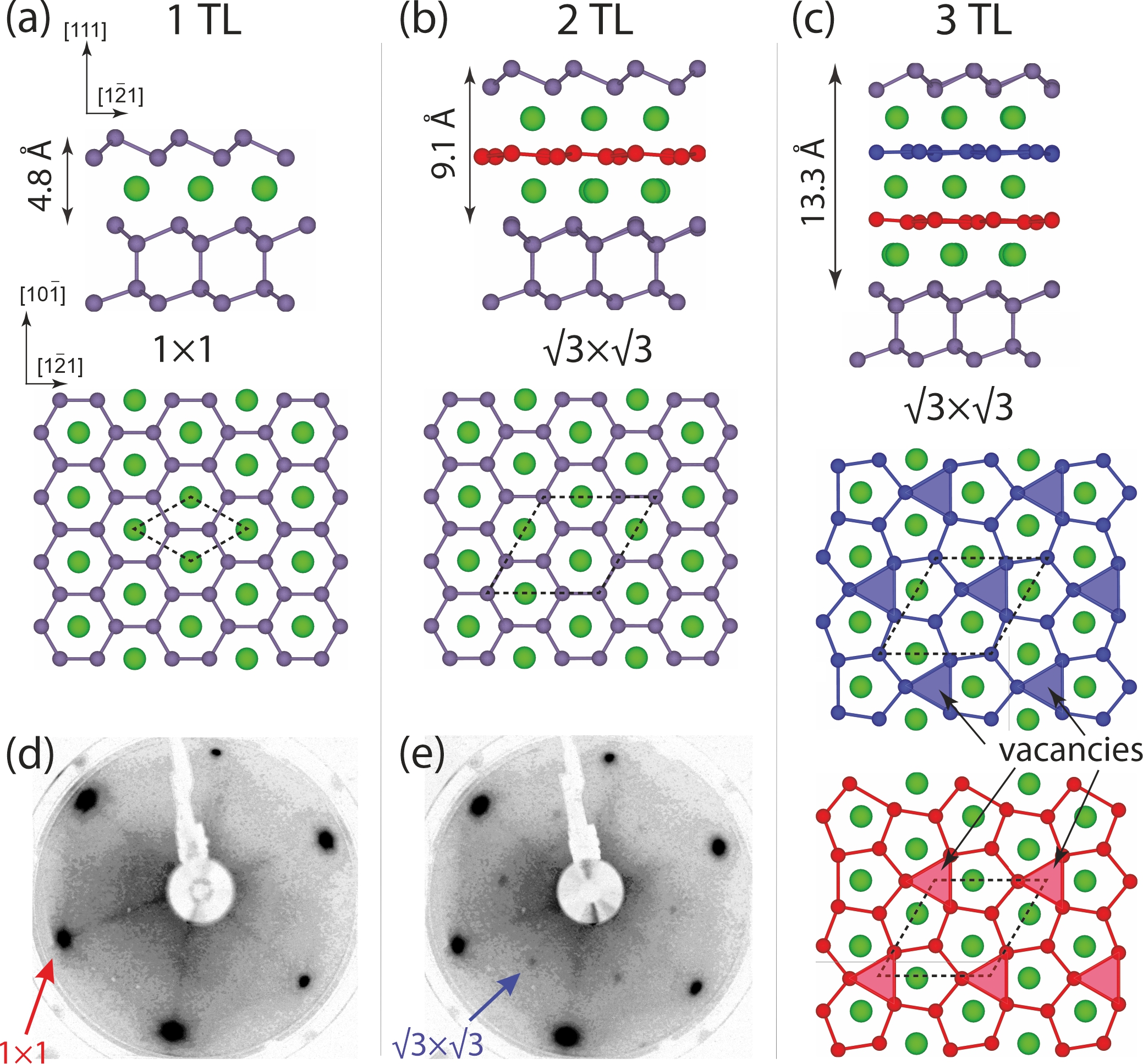
Trivalent rare-earth elements form germanides and silicides of various stoichiometries 20. In the present paper we will study defective AlB22 type ultrathin Gd germanide metalloxene films. Figure 1(a-c) shows the relaxed crystallographic structures of 1-3 TL films on Ge(111) obtained by the ab initio random structure searching (AIRSS) method 42. The atomic structure of the 1 TL GdGe2 (Fig. 1(a)) corresponds to the one reported previously in the literature 43, 23, 28. It consists of a single layer of Gd atoms sandwiched between the Ge(111) substrate and the buckled Ge surface bilayer (BL). This BL displays a reversed buckling with respect to the substrate. The 1 TL system has GdGe2 stoichiometry, hexagonal symmetry and 11 LEED pattern (Fig. 1(d)).
The formation of films thicker than 1 TL reduces the symmetry of the surface from hexagonal to trigonal and changes the surface periodicity from 11 to 23, as demonstrated by the emergence of weak reflexes in the LEED pattern (Fig. 1(e)). This weak periodicity was connected with the formation of the vacancy lattice in the inner semiconductor BLs of metalloxenes 44. Due to these vacancies the Ge BLs become almost flat (red and blue balls in Figs. 1(b, c)) and the overall stoichiometry of the inner TLs becomes Gd3Ge5. In spite of this change, for convenience we will use the GdGe2 notation for all Gd germanide films (we will adopt a similar nomenclature for Gd silicide and Dy germanide films), irrespectively of their thickness.
According to our calculations, the Gd atoms of the different layers are always located at the T4 site with reference to the underlying Ge(111) substrate. This is in line with previous high-angle annular dark-field transmission electron microscopy observations 28, 25. The geometry of the topmost Ge BL is the following: the upper Ge atom is located in the T1 site, while the lower Ge atom is located in the H3 site. For the 2 TL system the most energetically stable atomic configuration of the intermediate flat Ge layer has a vacancy defect located in one of the T1 sites. Importantly, the vacancy defects within flat Ge layers in 3 TL and thicker films have alternating positions with respect to the neighboring Ge layers, as shown in Fig. 1(c). The total thicknesses of 1, 2 and 3 TL GdGe2 films is 4.8, 9.1, and 13.3 Å, respectively.
3.2 Thickness-dependent electronic band structure of the GdGe2 films in the paramagnetic phase
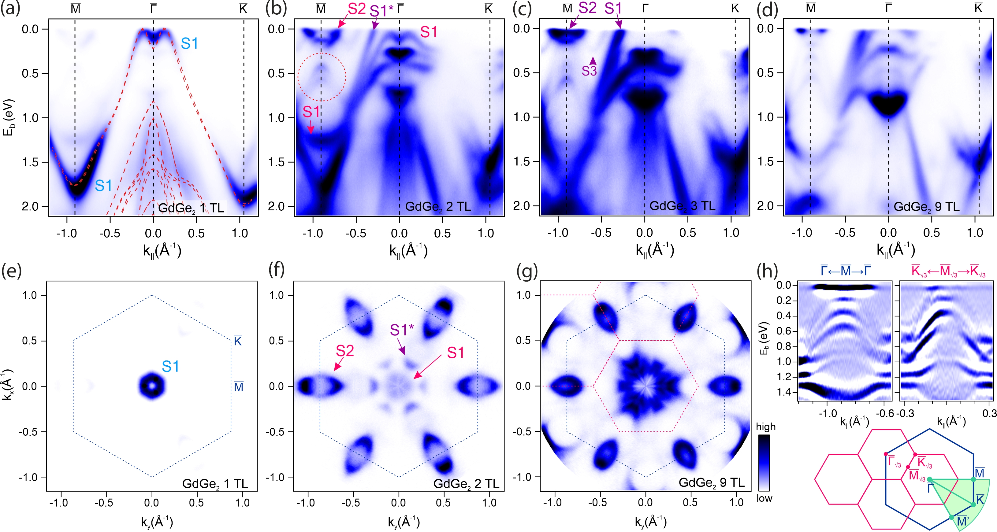
In this section we show ARPES data and DFT calculations for GdGe2 films of different thickness. The ARPES spectra for 1, 2, 3 and 9 (nominal) TL are shown in Figs. 2(a-d). Colored arrows and S1-S3 labels mark the characteristic features in the band structure that allow the identification of the film thickness and are discussed below in connection with the magnetic properties. The electronic structure of 1 TL (Fig. 2(a)) consists in the highly dispersive S1 surface band. This band is reproduced well by the DFT calculations for the 1 TL GdGe2 model previously discussed in section 3.1 (DFT results are overlaid onto the ARPES data in Fig. 2(a)). The Gd-Ge hybridization leads to the formation of the camel-like feature at the top of the S1 band, which touches the Fermi level and forms a ring-like hole pocket around the point (Fig. 2(e)).
The 2 TL GdGe2 film (Figs.2(b)) shows a S1 hole-like band similar to the 1 TL case. With respect to 1 TL, it is shifted to slightly higher binding energies at and by 0.5 eV towards lower energies at the point and is fully occupied. Additionally, a new S2 band leads to the formation of the electron pocket around the points (Figs.2(b,f)). Below this pocket a faint cone-like feature appears (marked by red circle in Figs.2(b)). A metallic band labeled S1∗ is observed along the direction. According to the calculation in Fig.S1 of the Electronic Supplementary Information (ESI) and Fig.4(e) it is associated to the 3 TL film and, therefore, is a manifestation of the coexistence of multiple thickness above the completion of 1 TL. Further confirmation of this assignment comes from the fact that at the nominal coverage of 3 TL the intensity of the S1 band, whose dispersion coincides with S1∗, is much stronger (Fig.2(c)). Here, a weak electron pocket labeled S3 can be observed between and .
In thicker films (Fig.2(d, g)) the spectrum in the vicinity of Fermi level is characterized by the presence of electron-like bands near the point and hole-like bands near the point. The apex of the cone-like band in point shifts towards lower binding energies with thickness and start to hybridize with the S2-like bands. This feature follows the vacancy-associated super-periodicity and can be found also in points (Fig.2(h)). Therefore, while the hole pockets around point and electron pockets in the points remain dominant, the spectral intensities in thicker films display additional features associated with the lattice which may be seen in the ARPES plot and Fermi surface map (Fig.2(g)).
3.3 Transition temperature and magnetic order of the GdGe2 films
In order to study the magnetic order and the effect of magnetism on the electronic structure of the GdGe2 films, we performed comprehensive ab initio calculations. The magnetic ground state of the Gd germanide system was determined by calculating the total energies for various magnetic configurations (see Tab. 1). Collinear in-plane AFM (cl AFM∥) represent the ground state for the multilayered films. The out-of-plane collinear AFM (cl AFM) configuration is less favorable by 0.2 meV per Gd atom. While the difference in total energy between cl AFM∥ and cl AFM is small it is enough to judge on magnetic ground state. The in-plane non-collinear 120∘ AFM (ncl 120∘ AFM∥) has 5 meV higher energy than the ground state. Finally, the in-plane FM (FM∥) and out-of-plane FM (FM) configurations are much less favorable than cl AFM∥. For 1 TL GdGe2 film, FM∥ is the ground state and is lower than FM by 0.5 meV.
| cl AFM∥ | cl AFM | ncl 120∘ AFM∥ | FM∥ | FM |
|---|---|---|---|---|
| 0.0 | 0.2 | 5.0 | 10.0 | 11.0 |
Let us now examine the effect of magnetism on the electronic band structure of the GdGe2 films by temperature-dependent ARPES and magnetic DFT calculations. We did not find any evidence of the magnetic behavior in the 1 TL GdGe2 film down to 14 K. We did not observe any magnetically-induced splitting of the S1 surface band or any other band structure changes, which were predicted by the band structure calculations in the FM∥ phase (Fig.S1, ESI). Therefore we come to the conclusion that the Curie temperature for the 1 TL lays below 14 K, in line with the magnetic measurements 45.
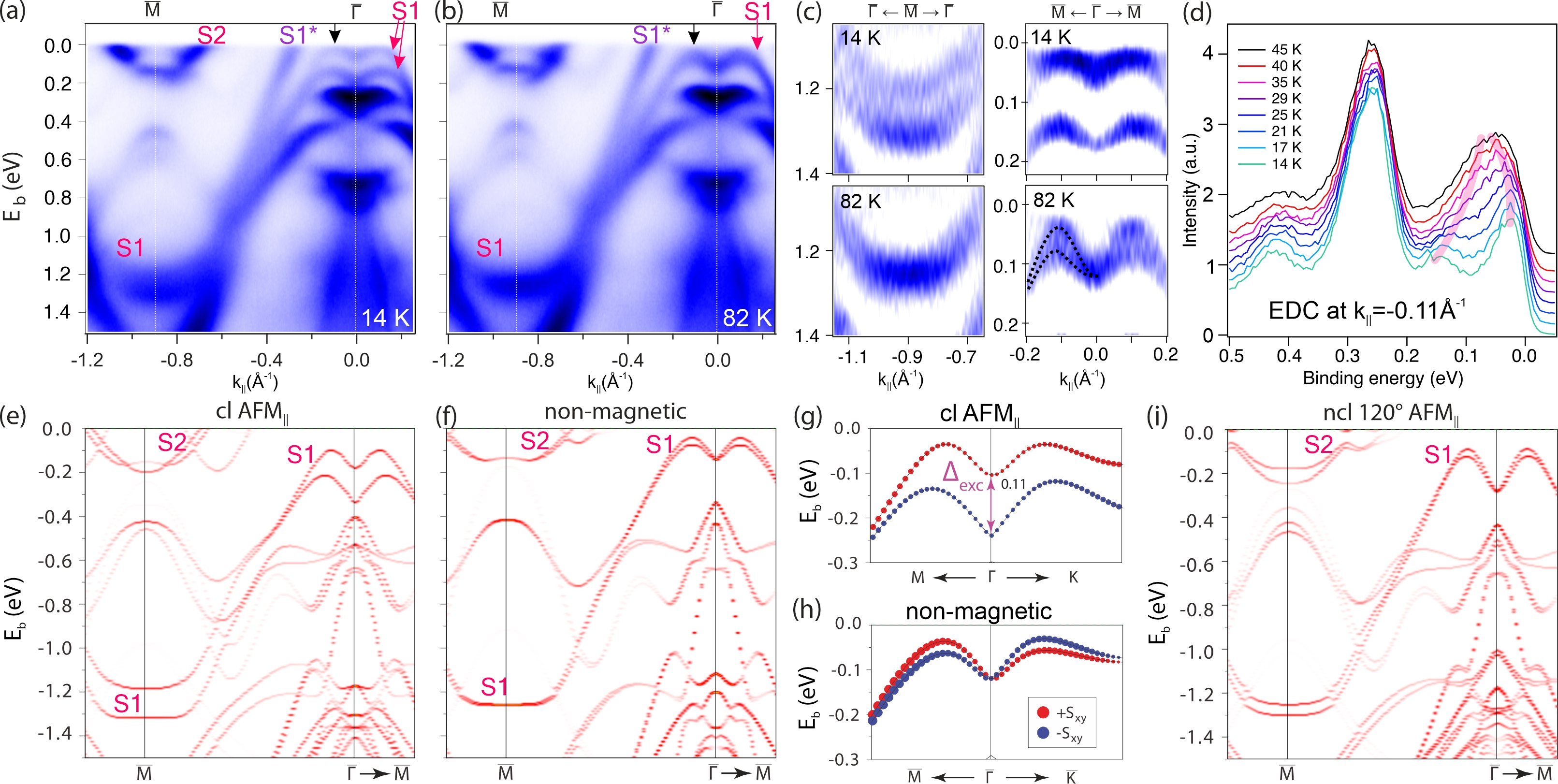
We made a temperature-dependent ARPES measurements for the 2 TL GdGe2 across the transition temperature reported in Ref.28 and investigated the behavior of the S1 and S2 bands. Figures 3(a, b) show the experimental spectra recorded at 14 and 82 K, respectively. At 14 K the S1 band displays a magnetic spin splittings of 130 meV at the point just below the Fermi level and of 100 meV at the point at E1.25 eV. Both splittings can be resolved in the second derivative spectra shown in Fig. 3 (c). When the temperature is raised up to 82 K, the above mentioned spin splittings at and disappear, while a tiny k-dependent splitting can still be observed near the point (Fig.3(c)). Instead, the S2 state does not show any significant change with temperature. Thus, to track the magnetic transition of the 2 TL film we use the temperature dependence of the splitting of the S1 state near the point. According to ARPES measurements made within the [1445] K temperature range the Néel transition temperature in 2 TL GdGe2 film is 311 K (fitting results for the exchange splitting value in Fig.S2 deduced from energy distribution curves in Fig. 3(d)). This indicates that already at the thickness of 2 TLs the GdGe2 film has a transition temperature that is close to the bulk value 20.
The band structure calculation for the cl AFM∥ and non-magnetic phases are shown in Figs. 3(e, g) and Figs. 3(f, h), respectively, while the band structure for the ncl 120∘ AFM∥ phase is shown in Fig. 3(i). It should be noted that the unfolding procedure 46, 47 was used for comparison of the experimental and calculated band structures, since collinear and ncl 120∘ AFM∥ band structures calculations require different unit cells. Namely, the cl AFM∥ and non-magnetic band structures initially calculated within the and supercells, respectively, were then unfolded onto the 11 surface BZ. DFT calculations for cl AFM∥ configuration (Fig. 3(e)) perfectly reproduce the low-temperature features of the experimental electron dispersion (Fig. 3(a)). The magnitude of the calculated exchange splitting of the S1 band at the point is equal to 110 meV (Fig. 3(e, g)), which is very close to the ARPES observation of 130 meV at 14 K. Similarly, the calculated splitting of the S1 band at the point is 130 meV (Fig. 3(e)) which is also close to the ARPES-derived value (100 meV). The energy splittings predicted by DFT for the S2 state and for the cone-like feature at are difficult to resolve by ARPES due to low intensity and a significant overlap with the 3 TL-derived features. The calculation for the non-magnetic case (Gd orbitals are treated as core states) reproduces perfectly the experimental observation at temperatures above the magnetic transition (Fig. 3(f)). The S1 band demonstrates a Rashba-like spin splitting 48 in the vicinity of the point with vortical spin-texture (Fig. 3(h)). This Rashba-like spin splitting can be observed in the second derivative of 82 K ARPES spectrum in Fig. 3(c). Instead, the band structure for the ncl 120∘ AFM∥ magnetic configuration (Fig. 3(i)) does not show any significant exchange splitting for the S1 band at the point. This supports the total energy calculation results that ncl 120∘ AFM∥ magnetic configuration is not a ground state.
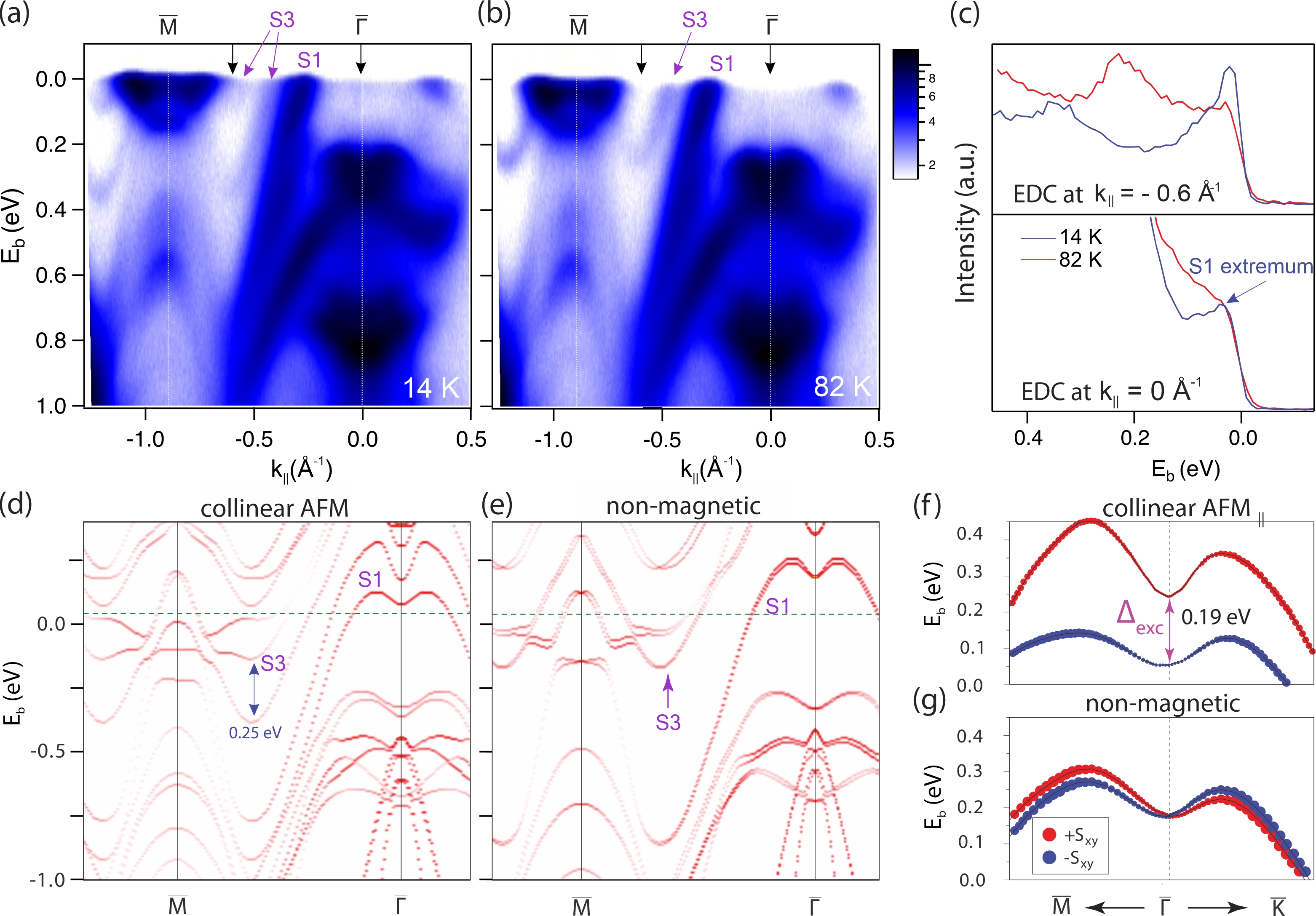
Interestingly, the energy position of the exchange-split camel-like feature at varies strongly with thickness. In the 3 TL GdGe2 film it is located above the Fermi level (Figs.4(a,d) and the S1 band is not fully occupied, in contrast to the 2 TL GdGe2 film. The magnetic transition here can still be traced experimentally by analyzing the band structure evolution with temperature. The S3 band forms an electron pocket between and points with a minimum at k||=0.6 Å-1 and exhibit exchange splitting: in the 14 K data there are two pockets separated by 270 meV with the lower branch minimum at 340 meV (Fig. 4 (a)), while in the 82 K data there is single pocket with the minimum at 250 meV (Fig.4(b)). The S3 band behavior in k||=0.6 Å-1 can be better visualized in the top panel of Fig. 4(c). Another difference between the low and high temperature spectra is the appearance of a faint intensity at the Fermi level near the point at 14 K that can be connected with the dip of the S1 band (bottom panel of Fig.4(c)). The behavior of these features at and k||=0.6 Å-1 is well reproduced by the calculations for the cl AFM∥ and non-magnetic phases (Fig. 4(d,e)), in close analogy to the case of the 2 TL films. Also for the 3 TL film the quenching of the exchange splitting of the S1 band near is accompanied by the appearance of Rashba-split bands with vortical spin-texture (Fig. 4(f,g)).
Notably, we did not observe explicit fingerprints of magnetic transition in the valence band structure of ultrathin DyGe2 and GdSi2 metalloxene films, which have the same crystallography structure of the GdGe2 films (Fig. S3). DyGe2 and GdGe2 show nearly identical band structures. Consistently with the fact that bulk Dy3Ge5 has T=7 K, our measurements on the 2 TL DyGe2 film at 14 K do not reveal any magnetically-induced band splitting. The band structure of the 2 TL GdSi2 film presents the same features of the corresponding GdGe2 film, with the only notable difference being the parabolic top of the S1 band at the point. Despite bulk Gd3Si5 has T=54 K 29, which is higher than the value for bulk Gd3Ge5 (T=38 K), the ARPES data for the 2 TL GdSi2 film do not display any signature of magnetically-induced band splitting. This behavior can be ascribed to the non-collinear AFM ground state of Gd3Si5 29, which is likely to have only minor influence on the band structure, as shown for the ncl 120∘ AFM∥ configuration of the 2 TL GdGe2 film (Fig. 3(i)).
3.4 Uncompensated magnetic moments in AFM GdGe2 films
| Atoms | p- | d- | f- | Total |
|---|---|---|---|---|
| Ge-BL | 0.045 | 0.000 | 0.000 | 0.045 |
| Gd 1-st layer | 0.010 | -0.136 | -6.917 | -7.042 |
| Ge-interlayer | 0.010 | 0.000 | 0.000 | 0.010 |
| Gd 2-nd layer | -0.010 | 0.159 | 6.919 | 7.072 |
| Ge(111)-BL | 0.020 | 0.000 | 0.000 | 0.020 |
As a final remark we want to address the discrepancy of our results with previously reported FM behavior in ultrathin metalloxene films 26. The 2 TL AFM GdGe2 film can display an uncompensated magnetic moment induced by orbital hybridization of Gd and Ge atoms. Indeed, the S1 band that exhibits the largest splitting in the vicinity of the Fermi level in the AFM state is localized on both Gd and surrounding Ge atoms (Fig. 1S). As shown in Tab. 2 the expectation value of the spin moment () of the first Gd layer is -7.042 , while of the second Gd layer equals to 7.072 resulting in the residual magnetic moment of 0.03 . The Ge BL residing on top of the structure has = 0.045 ; the of the upper Ge BL of the Ge(111) substrate is twice smaller, while of the intermediate Ge BL is four times smaller. Hence, the Ge-related contribution is provided by the orbitals and is always positive. As a result the total of the 2 TL GdGe2 is 0.105 in spite of the AFM ground state ordering. This tiny but non-zero value is in line with the small magnetic moment (compared to that of Gd) reported in the magnetic measurements for 2 TL thick metalloxene films 26. Another possible explanation for the reported FM behavior is the unavoidable inhomogeneity of the sample thickness that we observed directly in our samples and that was previously noticed in the scanning tunneling microscopy analysis of metalloxene films 23, 21. Space averaging investigation techniques, such as superconducting quantum interference device, can pick up signals from different film thickness, including the FM 1 TL, and attribute the FM ground state to films of larger (nominal) thickness.
4 Conclusions
Our study of ultrathin rare-earth GdGe2 metalloxenes films by ARPES measurements and comprehensive ab initio calculations shows in-plane FM order inside the single TL and AFM interlayer coupling. The hybridization between Gd and Ge orbitals induces a small uncompensated magnetic moment in the AFM-ordered films, which was previously associated with a FM ground state for these systems. The observed evolution of the GdGe2 band structure with thickness suggests that exchange-split bands can be tuned in a broad energy range, thus providing a viable way to design the magnetic properties of the films, also through the well-known doping techniques of semiconductor technology. Another interesting way to tune the magnetism in such systems is the incorporation of the metalloxene magnetic layers within semiconductor hetero-structures 49, which makes them promising candidates for 2D materials engineering, similar to that proposed for layered chalcogenides. Finally, the spin S, orbital L and total magnetic momenta J of the metalloxenes can be controlled by suitable choice of rare-earth elements that have similar valence states and ionic radius. All these aspects make metalloxens a convenient playground to study magnetism in the 2D limit.
Author Contributions
A. V. Matetskiy: Investigation, Conceptualization, Supervision, Writing - original draft, Writing - Review and Editing, Project administration. V. Milotti: Investigation, Formal analysis, Writing - Review and Editing. P. M. Sheverdyaeva: Investigation, Validation, Writing - Review and Editing. P. Moras: Investigation, Validation, Writing - Review and Editing. C. Carbone: Validation, Conceptualization. A. N. Mihalyuk: Software, Conceptualization, Visualization, Writing - original draft, Writing - Review and Editing.
Conflicts of interest
There are no conflicts to declare.
Acknowledgements
A. N. Mihalyuk acknowledge that DFT calculations were supported by the Russian Science Foundation (Grant No. 19-12-00101, https://rscf.ru/project/19-12-00101/). A. V. Matetskiy, P. M. Sheverdyaeva, P. Moras, C. Carbone acknowledge EUROFEL-ROADMAP ESFRI of the Italian Ministry of Education, University, and Research. The authors thank S.V. Eremeev for comments and helpful discussions. The calculations were conducted using the equipment of Shared Resource Center ”Far Eastern Computing Resource” IACP FEB RAS (https://cc.dvo.ru).
References
- Vedmedenko et al. 2020 E. Vedmedenko, R. Kawakami, D. Sheka, P. Gambardella, A. Kirilyuk, A. Hirohata, C. Binek, O. Chubykalo-Fesenko, S. Sanvito, B. Kirby, J. Grollier, K. Everschor-Sitte, T. Kampfrath, C.-Y. You and A. Berger, Journal of Physics D: Applied Physics, 2020, 53, 1–44.
- Jiang et al. 2021 X. Jiang, Q. Liu, J. Xing, N. Liu, Y. Guo, Z. Liu and J. Zhao, Applied Physics Reviews, 2021, 8, 031305.
- Burch et al. 2018 K. S. Burch, D. Mandrus and J. G. Park, Nature, 2018, 563, 47–52.
- Fei et al. 2018 Z. Fei, B. Huang, P. Malinowski, W. Wang, T. Song, J. Sanchez, W. Yao, D. Xiao, X. Zhu, A. F. May, W. Wu, D. H. Cobden, J. H. Chu and X. Xu, Nature Materials, 2018, 17, 778–782.
- Gong et al. 2017 C. Gong, L. Li, Z. Li, H. Ji, A. Stern, Y. Xia, T. Cao, W. Bao, C. Wang, Y. Wang, Z. Q. Qiu, R. J. Cava, S. G. Louie, J. Xia and X. Zhang, Nature, 2017, 546, 265–269.
- McGuire et al. 2015 M. A. McGuire, H. Dixit, V. R. Cooper and B. C. Sales, Chemistry of Materials, 2015, 27, 612–620.
- Huang et al. 2017 B. Huang, G. Clark, E. Navarro-Moratalla, D. R. Klein, R. Cheng, K. L. Seyler, D. Zhong, E. Schmidgall, M. A. McGuire, D. H. Cobden, W. Yao, D. Xiao, P. Jarillo-Herrero and X. Xu, Nature, 2017, 546, 270–273.
- Gibertini et al. 2019 M. Gibertini, M. Koperski, A. F. Morpurgo and K. S. Novoselov, Nature Nanotechnology, 2019, 14, 408–419.
- Peierls 1936 R. Peierls, Mathematical Proceedings of the Cambridge Philosophical Society, 1936, 32, 477–481.
- Mermin and Wagner 1966 N. D. Mermin and H. Wagner, Physical Review Letters, 1966, 17, 1133–1136.
- Hohenberg 1967 P. C. Hohenberg, Physical Review, 1967, 158, 383–386.
- Zhang et al. 2022 H. Zhang, D. Raftrey, Y. T. Chan, Y. T. Shao, R. Chen, X. Chen, X. Huang, J. T. Reichanadter, K. Dong, S. Susarla, L. Caretta, Z. Chen, J. Yao, P. Fischer, J. B. Neaton, W. Wu, D. A. Muller, R. J. Birgeneau and R. Ramesh, Science Advances, 2022, 8, 1–11.
- Liu et al. 2020 C. Liu, Y. Wang, H. Li, Y. Wu, Y. Li, J. Li, K. He, Y. Xu, J. Zhang and Y. Wang, Nature Materials, 2020, 19, 522–527.
- Ying et al. 2022 Z. Ying, S. Zhang, B. Chen, B. Jia, F. Fei, M. Zhang, H. Zhang, X. Wang and F. Song, Physical Review B, 2022, 105, 1–6.
- Deng et al. 2020 Y. Deng, Y. Yu, M. Z. Shi, Z. Guo, Z. Xu, J. Wang, X. H. Chen and Y. Zhang, Science, 2020, 367, 895–900.
- Ge et al. 2020 J. Ge, Y. Liu, J. Li, H. Li, T. Luo, Y. Wu, Y. Xu and J. Wang, National Science Review, 2020, 7, 1280–1287.
- Tokura and Kanazawa 2021 Y. Tokura and N. Kanazawa, Chemical Reviews, 2021, 121, 2857–2897.
- Kurumaji et al. 2019 T. Kurumaji, T. Nakajima, M. Hirschberger, A. Kikkawa, Y. Yamasaki, H. Sagayama, H. Nakao, Y. Taguchi, T. Arima and Y. Tokura, Science, 2019, 365, 914–918.
- Khanh et al. 2020 N. D. Khanh, T. Nakajima, X. Yu, S. Gao, K. Shibata, M. Hirschberger, Y. Yamasaki, H. Sagayama, H. Nakao, L. Peng, K. Nakajima, R. Takagi, T. Arima, Y. Tokura and S. Seki, Nature Nanotechnology, 2020, 15, 444–449.
- Westrum 1968 E. F. Westrum, Progress in the Science and Technology of the Rare Earths, Pergamon press, 1968.
- Engelhardt et al. 2006 I. Engelhardt, C. Preinesberger, S. Becker, H. Eisele and M. Dähne, Surface Science, 2006, 600, 755–761.
- Vandré et al. 1999 S. Vandré, T. Kalka, C. Preinesberger and M. Dähne-Prietsch, Phys. Rev. Lett., 1999, 82, 1927–1930.
- Wanke et al. 2009 M. Wanke, M. Franz, M. Vetterlein, G. Pruskil, B. Höpfner, C. Prohl, I. Engelhardt, P. Stojanov, E. Huwald, J. Riley and M. Dähne, Surface Science, 2009, 603, 2808–2814.
- Franz et al. 2016 M. Franz, S. Appelfeller, C. Prohl, J. Große, H.-F. Jirschik, V. Füllert, C. Hassenstein, Z. Diemer and M. Dähne, Journal of Vacuum Science & Technology A, 2016, 34, 061503.
- Parfenov et al. 2019 O. E. Parfenov, A. M. Tokmachev, D. V. Averyanov, I. A. Karateev, I. S. Sokolov, A. N. Taldenkov and V. G. Storchak, Materials Today, 2019, 29, 20–25.
- Tokmachev et al. 2019 A. M. Tokmachev, D. V. Averyanov, A. N. Taldenkov, O. E. Parfenov, I. A. Karateev, I. S. Sokolov and V. G. Storchak, Materials Horizons, 2019, 6, 1488–1496.
- Averyanov et al. 2020 D. V. Averyanov, I. S. Sokolov, M. S. Platunov, F. Wilhelm, A. Rogalev, P. Gargiani, M. Valvidares, N. Jaouen, O. E. Parfenov, A. N. Taldenkov, I. A. Karateev, A. M. Tokmachev and V. G. Storchak, Nano Research, 2020, 13, 3396–3402.
- Tokmachev et al. 2019 A. M. Tokmachev, D. V. Averyanov, A. N. Taldenkov, O. E. Parfenov, I. A. Karateev, I. S. Sokolov and V. G. Storchak, Materials Horizons, 2019, 6, 1488–1496.
- Roger et al. 2006 J. Roger, V. Babizhetskyy, K. Hiebl, J. F. Halet and R. Guérin, Journal of Alloys and Compounds, 2006, 407, 25–35.
- Pakhira et al. 2023 S. Pakhira, A. K. Kundu, F. Islam, M. A. Tanatar, T. Roy, T. Heitmann, T. Yilmaz, E. Vescovo, M. Tsujikawa, M. Shirai, R. Prozorov, D. Vaknin and D. C. Johnston, Phys. Rev. B, 2023, 107, 134439.
- Chikina et al. 2014 A. Chikina, M. Höppner, S. Seiro, K. Kummer, S. Danzenbächer, S. Patil, A. Generalov, M. Güttler, Y. Kucherenko, E. V. Chulkov, Y. M. Koroteev, K. Köpernik, C. Geibel, M. Shi, M. Radovic, C. Laubschat and D. V. Vyalikh, Nature Communications, 2014, 5, 1–7.
- Schmitt et al. 2019 M. Schmitt, P. Moras, G. Bihlmayer, R. Cotsakis, M. Vogt, J. Kemmer, A. Belabbes, P. M. Sheverdyaeva, A. K. Kundu, C. Carbone, S. Blügel and M. Bode, Nature Communications, 2019, 10, 1–6.
- Elmers et al. 2023 H. J. Elmers, S. Haldar, K. Medjanik, S. Babenkov, O. Fedchenko, D. Vasilyev, S. Heinze and G. Schönhense, Phys. Rev. B, 2023, 107, 144424.
- Lee et al. 2023 K. Lee, N. H. Jo, L.-L. Wang, R. A. Ribeiro, Y. Kushnirenko, B. Schrunk, P. C. Canfield and A. Kaminski, Journal of Physics: Condensed Matter, 2023, 35, 245501.
- Eremeev et al. 2023 S. V. Eremeev, D. Glazkova, G. Poelchen, A. Kraiker, K. Ali, A. V. Tarasov, S. Schulz, K. Kliemt, E. V. Chulkov, V. S. Stolyarov, A. Ernst, C. Krellner, D. Y. Usachov and D. V. Vyalikh, Insight into the electronic structure of the centrosymmetric skyrmion magnet GdRu2Si2, 2023.
- Fernandez et al. 2020 L. Fernandez, M. Blanco-Rey, R. Castrillo-Bodero, M. Ilyn, K. Ali, E. Turco, M. Corso, M. Ormaza, P. Gargiani, M. A. Valbuena, A. Mugarza, P. Moras, P. M. Sheverdyaeva, A. K. Kundu, M. Jugovac, C. Laubschat, J. E. Ortega and F. Schiller, Nanoscale, 2020, 12, 22258–22267.
- Kresse and Hafner 1993 G. Kresse and J. Hafner, Physical Review B, 1993, 47, 558–561.
- Blöchl 1994 P. E. Blöchl, Physical Review B, 1994, 50, 17953–17979.
- Perdew et al. 1996 J. P. Perdew, K. Burke and M. Ernzerhof, Physical Review Letters, 1996, 77, 3865–3868.
- Kresse and Joubert 1999 G. Kresse and D. Joubert, Physical Review B, 1999, 59, 1758–1775.
- Krukau et al. 2006 A. V. Krukau, O. A. Vydrov, A. F. Izmaylov and G. E. Scuseria, The Journal of Chemical Physics, 2006, 125, 224106.
- Pickard and Needs 2011 C. J. Pickard and R. J. Needs, Journal of physics. Condensed matter, 2011, 23, 053201.
- Sanna et al. 2021 S. Sanna, J. Plaickner, K. Holtgrewe, V. M. Wettig, E. Speiser, S. Chandola and N. Esser, Materials, 2021, 14, 4104.
- Wetzel et al. 1996 P. Wetzel, S. Saintenoy, C. Pirri, D. Bolmont, G. Gewinner, T. P. Roge, F. Palmino, C. Savall and J. C. Labrune, Surface Science, 1996, 355, 13–20.
- Tokmachev et al. 2018 A. M. Tokmachev, D. V. Averyanov, O. E. Parfenov, A. N. Taldenkov, I. A. Karateev, I. S. Sokolov, O. A. Kondratev and V. G. Storchak, Nature Communications, 2018, 9, 1672.
- Medeiros et al. 2014 P. V. C. Medeiros, S. Stafström and J. Björk, Phys. Rev. B, 2014, 89, 041407.
- Medeiros et al. 2015 P. V. C. Medeiros, S. S. Tsirkin, S. Stafström and J. Björk, Phys. Rev. B, 2015, 91, 041116.
- Bihlmayer et al. 2022 G. Bihlmayer, P. Noel, D. V. Vyalikh, E. V. Chulkov and A. Manchon, Nature Reviews Physics, 2022, 4, 642–659.
- Bondarenko et al. 2021 L. V. Bondarenko, A. Y. Tupchaya, Y. E. Vekovshinin, D. V. Gruznev, A. N. Mihalyuk, D. A. Olyanich, Y. P. Ivanov, A. V. Matetskiy, A. V. Zotov and A. A. Saranin, ACS Nano, 2021, 15, 19357–19363.