Pseudo Electric Field and Pumping Valley Current in Graphene Nano-bubbles
Abstract
Abstract: The extremely high pseudo-magnetic field emerging in strained graphene suggests that an oscillating nano-deformation will induce a very high current even without electric bias. In this paper, we demonstrate the sub-terahertz (THz) dynamics of a valley-current and the corresponding charge pumping with a periodically excited nano-bubble. We discuss the amplitude of the pseudo-electric field and investigate the dependence of the pumped valley current on the different parameters of the system. Finally, we report the signature of extra-harmonics generation in the valley current that might lead to potential modern devices development operating in the nonlinear regime.
1 INTRODUCTION
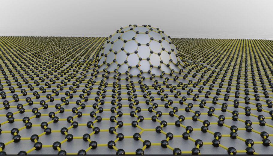
An interesting and powerful property of graphene is its ability to be stretched elastically up to 25, and to control the induced strains in different ways [1, 2]. In addition, the unique coupling between mechanical deformation and electronic structure along with the possibility of deformation makes graphene attracts considerable attention [3, 4]. This interplay was examined by observing the Landau levels that can form in graphene due to an induced strain [4]. Indeed, deformed graphene (Fig. 1) can generate an effective gauge field [4], to which one can associate a pseudo magnetic field (PMF), . This stimulated pseudo magnetic field would allow electrons to behave as if they were subjected to a strong real magnetic field with strength a few orders of magnitude higher than the one generated by superconducting magnets. [5].
Currently, there is a great interest in generating and controlling the valley degree of freedom of electrons in semiconductors. Indeed, the ability to manipulate valley electrons can potentially enable advanced valley-resolved electronic devices. In particular, this valley controllability opens up the possibility of using the momentum state of electrons, holes, or excitons as a completely new paradigm in information processing [6]. Moreover, pure valley currents are interestingly non-dissipative currents with no accompanying net charge flow, akin to pure spin currents [7]. This property is very useful in seeking ultra-low power devices. Different routes have been proposed for generating valley currents such as using quantum pumps with a Dirac gap [8], and using electrically induced Berry curvature in bilayer graphene [7].
In the quantum pumping technique, a cyclic change of the AC voltage of the gates leads to the variation in the scattering matrix of the device and the generation of a DC current [8]. This method of generating a charge DC current without bias voltage between two electrodes [9, 8] can be generalized to account for the spin or even the valley degree of freedom. In this work, a time-dependent nano-bubble in graphene, that can be created by a time-dependent voltage of an Atomic Force Microscopy (AFM) tip, capacitively coupled to the device [10], will be utilized as a quantum pumping device to examine the possibilities of generating a nonzero valley current with a zero net charge current.
The deformation itself can be initially created by different techniques such as corrugated substrate engineering [11, 12] or gas inflation [13].
The pseudo magnetic field associated with the deformation in graphene is valley dependent and changes its sign between the two valley points K and K’.This feature allows the PMF to preserve time-reversal symmetry unlike a real external magnetic field. Consequently, a time manipulation of the PMF will induce different behaviour for the K and K’ electrons and thus a valley-resolved study of the current is necessary [14].
It is worth mentioning that different studies have looked at the effect of other dynamical strains on the electronic transport. Ref. [15] for example, considered in-plane strain in a gapped graphene to induce a topological current, Ref. [16] looked at the symmetry requirements for pumping valley current, while Ref. [17] investigated the pseudo quantum Hall regime due to strain. Other shapes or mechanisms to get the valley filtering were also investigated [18, 19]
2 MODEL
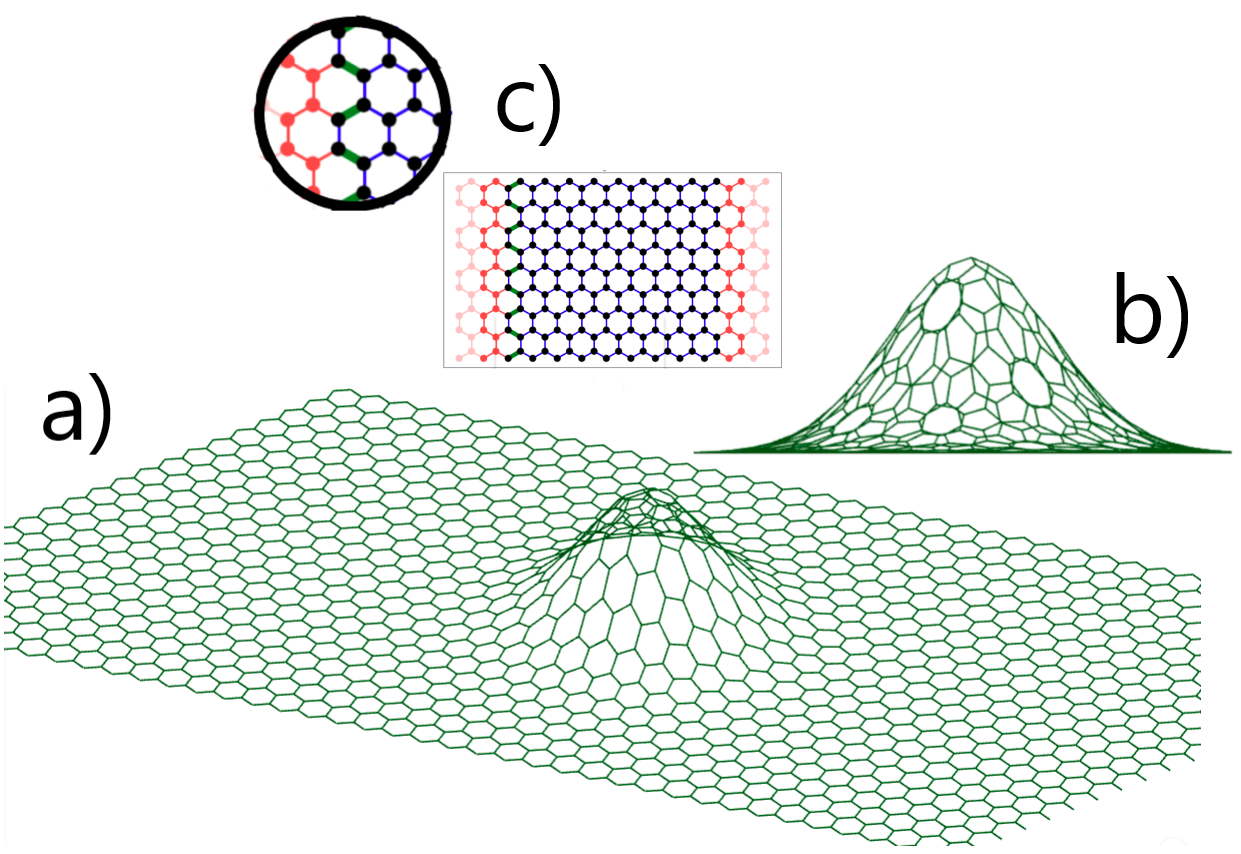
Graphene consists of carbon atoms, that are arranged in an hexagonal honeycomb structure. This arrangement is a triangular lattice with a basis of two atoms per unit cell where the lattice vector for this structure are and (Fig. 2) and the constant a is carbon-carbon distance with value 1.42 [21]. The electronic structure of strained graphene is studied by utilizing a first nearest neighbor tight-binding model approximation, where the sum runs over the nearest neighboring atoms. Figure 2 shows the semi-infinite graphene system, where the plane waves are coming along the zigzag direction from left and right leads. Experimentally, the deformation can be created in a graphene sheet by using an atomic force microscope’s tip [10, 22, 23]. In the presence of a nano-bubble the nearest neighbors hopping parameters become all different. Thus, the strain can be included in the system by altering the hopping parameter to the strained bond length. The adjustment of the hopping in the presence of the strain can be described by
| (1) |
where , for graphene structure [24]. represents the length of the strained lattice bonds whereas is the lattice constant in the absence of strain.
3 RESULTS
3.1 Pseudo Magnetic Field
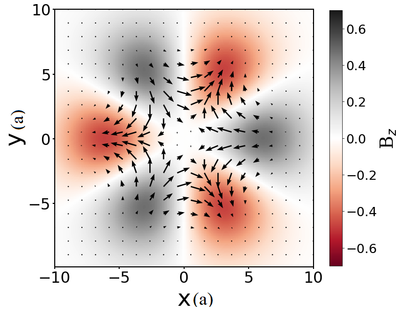
In our model, the graphene out-of-plane deformation is local with a characteristic width , a maximum height [4, 25, 3] and an overall Gaussian shape modeled by . In the limit of low-energy carriers, the deformation is equivalent to an induced effective vector potential given by [1] , where the stress tensors can be calculated by . A straightforward calculation leads to the following form of the vector potential,
| (2) |
The corresponding pseudo magnetic field can be obtained by :
| (3) |
The pseudo magnetic field shows alternating positive and negative regions in the deformation position as shown in Fig. 3. This magnetic field is valley dependent and changes its sign between the high symmetry points and and is responsible for the valley filtering in graphene nano-bubbles [3].
Using eq.1, we can demonstrate that the maximum relative change in the hopping parameter is proportional to . This implies that for a small deformation width , it becomes necessary to reduce the maximum height to remain within the constraints of stretchable graphene [1, 2]. In our particular case, a numerical examination of max() confirms that we are, indeed, within this specified limit.
3.2 Induced Pseudo Electric Field
The dynamics of the charge carriers in graphene under a dynamical external mechanical strain is a challenging problem. The generated frequencies of the perturbation projects into the sub-Terahertz domain with reported frequencies up to 200 GHz [26]. We note in passing that such frequencies are much smaller than the bandwidth of graphene. Therefore, standard techniques like Floquet theory [27, 28, 29, 30, 31, 32, 33] are hard to apply, which makes a full numerical treatment necessary and which will be the subject of our work. Things become more interesting when the strain is a nano-bubble exhibiting a few hundred Teslas pseudo magnetic field. Indeed, an oscillating bump with a height will change the vector potential to a new form . In the Weyl gauge, the Maxwell equations show an induced pseudo electric field in the limit , to the lowest order:
| (4) |
where the dot represents the time derivative. This result accounts for the small perturbations due to a small amplitude in the out-of-plane vibration of the nano-bubble which allows us to keep our interpretation within the linear response theory. It is worth noting that although the pseudo magnetic field is strong (hundreds of Teslas), the induced electric field is only a few kV/cm. This is mainly explained by the fact that these large values of are rather due to the large gradient of (variation on very short scales) than to its magnitude. The pseudo-electric field map is depicted in Fig. 3 where a threefold symmetry emerges and the system alternates between an inward and outward pseudo electric field for the and valleys.
3.3 Charge and Valley Currents
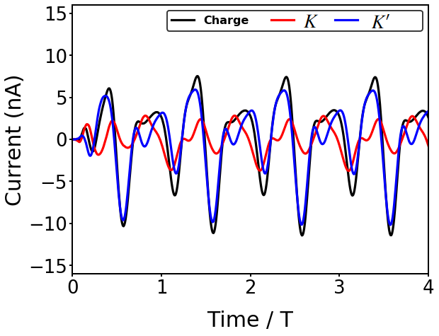
As, in the case of charge-pumping by the dynamics of a skyrmion deformation [34, 9] and spin-pumping by the precession of magnetic textures [35, 36], an oscillating nano-bubble is expected to alter the charge density and induce a charge/valley current through the interface between the system and the lead [37]. To investigate this property, we adopt a nano-bubble oscillating at hundreds GHz with with a height modulation strength , a characteristic width and a perturbation magnitude . The way to generate these oscillations is unimportant at this stage but can be initiated by a capacitively coupled atomic force microscope’s tip or a laser on top of the strained part. The first step towards the calculation of the charge current is to solve the time-dependent Schrodinger equation to obtain the wave functions at different times and then calculate the different currents in the system in one-body formalism [38, 39]. It is important to mention that a more accurate procedure involves an integration over the different contributions from all energies in the Fermi sea. This was safely avoided due to the small driving frequencies (compared to the Fermi level ) and the small excitations considered in this study (). This reduces the needed numerical resources and keeps the problem at the Fermi surface (similar to the case of the spin-pumping theory). Figure 4 shows the result of the pumped charge current , which expectedly averages to zero as explained by the scattering approach to parametric pumping. Indeed, varying one parameter is not enough to generate a sustainable charge current [9].
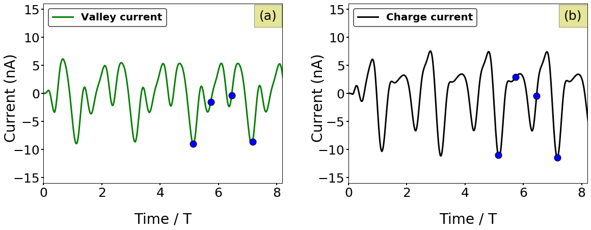
The frequency of the signal is the same as that of the oscillating nano-bubble. So far, these results look like the same as for the spin pumping of , and in Ferromagnets (precessing around the z-axis): zero average and the same frequency as the driving perturbation. Since the pseudo electric field is valley dependent, the contribution coming from each K-point to the charge current is investigated and plotted in Fig. 4. The two currents, , and have amplitudes of the same order of magnitude and both oscillate at the same angular frequency . The two currents are not exactly the same, because for a Fermi energy slightly higher than zero, the modes in the two different valleys are non-symmetric and have slightly different wavenumbers. The valley current, which is defined as is of huge interest in low energy consumption devices. The reason behind it is that the net charge transferred can be zero whereas at the same time the valley current is not vanishing. This eliminates the dissipation of energy as heat while transporting information through the valleys’ degrees of freedom. The valley current is well defined in the interface region (away from the bubble), because the lead is uniform and the conducting modes (incoming wave functions from the lead) do not mix. One has to compute the time-dependent wave function for each mode, using T-kwant package [38, 39], and identify the different modes in each valley. The contribution of each mode to the current between sites and reads:
| (5) |
where, is the wave function of a given mode at site . is the matrix element between sites a and b (in our case, it represents the hopping parameter between a and b in graphene). The contribution of modes of a given valley are summed together to finally express . Inside the scattering region, this procedure can still be used, but the current is not exactly a pure valley current. Indeed, the scattering between the valleys is possible, yet it remains small (the points K and K’ are far apart in the Brillouin zone) [14]. For this reason, the approximation of the local current in the scattering region is still valid [14]. Another approach is to project the wave functions on the valley-resolved ones of pristine graphene [24].
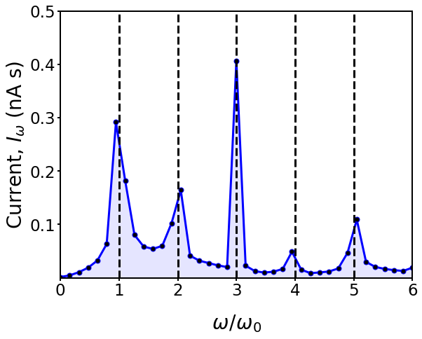
Fig. 5 shows the result for the valley current pumped through the same interface. The average is again zero and the amplitude is much smaller than that of the charge current. The most important thing to notice is that the frequency of the is not exactly the same as that of the nano-bubble. As we can see in Fig. 7, the valley current exhibits a main frequency of with small contributions from , and . The appearance of higher-order harmonics was recently reported for spin-pumping in the presence of spin-orbit interaction [40] or in the presence of non-collinear magnetic structure [41]. In our case, none of the discussed causes in [40, 41] are present in our system.
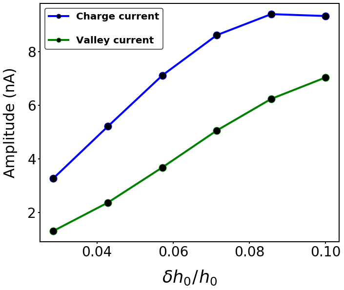
The charge and valley pumping depend on the parameters of the system. As we can see it from the expression of the pseudo electric field, the latter is proportional to the perturbation . Naturally, this is expected to be the same for the charge and valley currents. Fig. 7 b) shows the amplitude of the and which are clearly linearly varying with the change . For stronger perturbations, higher non-linear effects are expected to manifest. Another way to increase the different pumped currents is to play with the frequency and use a Terahertz spectrum. This is a challenging task, but very promising results suggest that this projection is reachable [26]. The zero-average of the valley current makes it very difficult to exploit in devices since no accumulation can be obtained and only oscillating current redistribution of the valleys is achieved. With proper engineering, we still can think of it as the basis for a potentially new Field-effect transistor [42].
3.4 Local currents
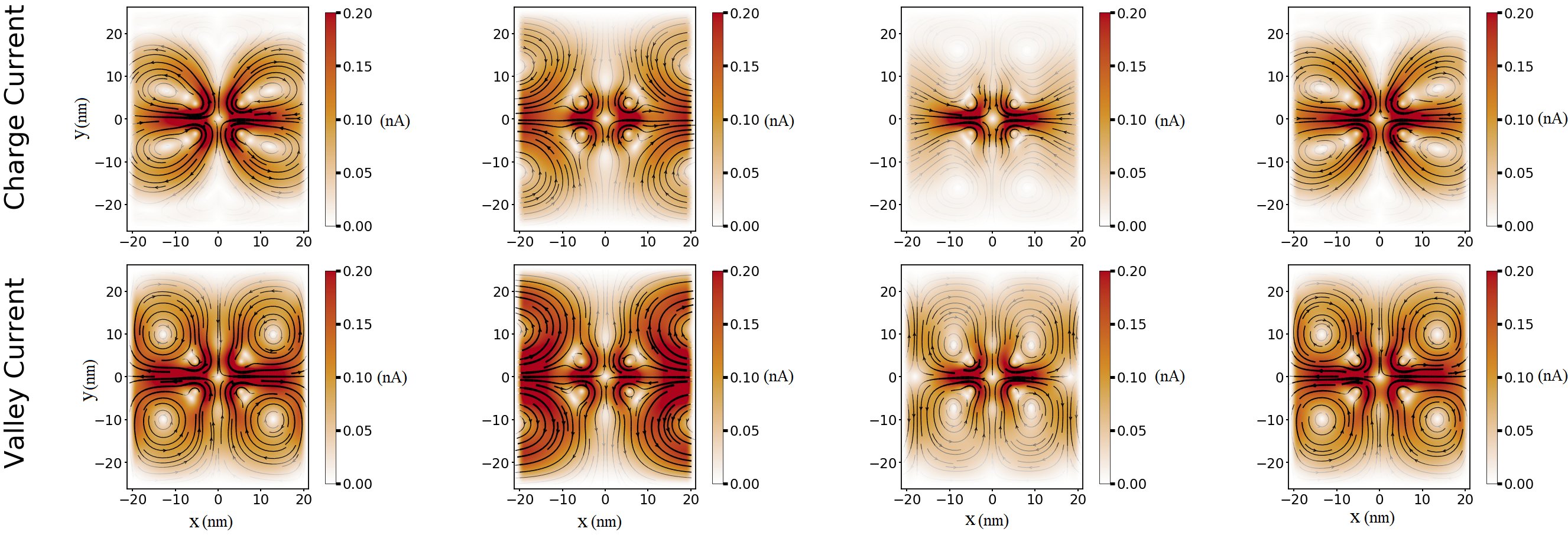
Since the pseudo electric field is local and mainly appears in the central system, investigating the current at different regions than the interface with the lead might be of a great interest. The plot of the current map will show how the regions of the maximum pseudo magnetic field influence the current direction and generation. The wave functions are calculated at all sites of the systems which allows us to express the local currents. Fig. 6 illustrates the map obtained at different times during one period. The current lines for the charge and the valley are symmetric which is just the reflection of the symmetry of the Gaussian bump considered in this work. This will be different if a triaxial strain was adopted. In fact, it is known that a Gaussian deformation filters the valleys whereas the triaxial one splits them [3]. The Fermi energy is chosen low to reduce the number of modes due to the limited computing resources in this kind of 2D maps (current is calculated between each two links, at each time) and this doesn’t change the general conclusions. The maps for the valley current and the charge current are intrinsically different: for the charge current, it is hard to see the positions of the valley-dependent maxima of the pseudo-magnetic field. The situation is different for the valley current. We clearly notice loops of different orientations showing the dependence of the pseudo-magnetic field on the valley of the carriers. The size of the current’s loops can be changed via the parameter ie, creating very peaked bumps or smoothly varying ones over a larger region. The number of modes for the chosen Fermi energy is very small. In order to increase the current, one needs to increase it either by changing the width of the system or by increasing the Fermi energy.
It’s worth mentioning that we did investigate deformations with elliptical symmetry,
deliberately tilting them to disrupt left-right symmetry. Unfortunately, this approach did not lead to
a sustained average valley current.
CONCLUSION
The pseudo magnetic field generated by a strained graphene sheet was analyzed. In the presence of a time-dependent oscillating strain, a corresponding pseudo electric field is stimulated giving rise to a redistribution of the quantum states in momentum space, leading to charge and valley pumping. We demonstrated that the valley current exhibits extra-harmonics and that on average, the pseudo electric field did not sustain a direct current, and rather a zero average was obtained. This work opens the door to further interesting studies like the pseudo-electric field generated by the propagation of mechanical waves in graphene or the distribution of local electric currents due to phonons and temperature effects on graphene.
ACKNOWLEDGMENT
The authors acknowledge computing time on the supercomputer SHAHEEN at KAUST Supercomputing Centre and the team assistance. A.A. and M.V. gratefully acknowledge the support provided by the Deanship of Research Oversight and Coordination (DROC) at King Fahd University of Petroleum and Minerals (KFUPM) for funding this work through exploratory research grant No. ER221002.
REFERENCES
- Masir et al. [2013] M. R. Masir, D. Moldovan, and F. Peeters, Pseudo magnetic field in strained graphene: Revisited, Solid state communications 175, 76 (2013).
- Guinea et al. [2010a] F. Guinea, A. Geim, M. Katsnelson, and K. Novoselov, Generating quantizing pseudomagnetic fields by bending graphene ribbons, Physical Review B 81, 035408 (2010a).
- Settnes et al. [2016] M. Settnes, S. R. Power, M. Brandbyge, and A.-P. Jauho, Graphene nanobubbles as valley filters and beam splitters, Physical review letters 117, 276801 (2016).
- De Juan et al. [2011] F. De Juan, A. Cortijo, M. A. Vozmediano, and A. Cano, Aharonov–bohm interferences from local deformations in graphene, Nature Physics 7, 810 (2011).
- Guinea et al. [2010b] F. Guinea, M. Katsnelson, and A. Geim, Energy gaps and a zero-field quantum hall effect in graphene by strain engineering, Nature Physics 6, 30 (2010b).
- Vitale et al. [2018] S. A. Vitale, D. Nezich, J. O. Varghese, P. Kim, N. Gedik, P. Jarillo-Herrero, D. Xiao, and M. Rothschild, Valleytronics: opportunities, challenges, and paths forward, Small 14, 1801483 (2018).
- Shimazaki et al. [2015] Y. Shimazaki, M. Yamamoto, I. V. Borzenets, K. Watanabe, T. Taniguchi, and S. Tarucha, Generation and detection of pure valley current by electrically induced berry curvature in bilayer graphene, Nature Physics 11, 1032 (2015).
- Wang et al. [2014] J. Wang, Z. Lin, and K. S. Chan, Pure valley current generation in graphene with a dirac gap by quantum pumping, Applied Physics Express 7, 125102 (2014).
- Brouwer [1998] P. Brouwer, Scattering approach to parametric pumping, Physical Review B 58, R10135 (1998).
- Klimov et al. [2012] N. N. Klimov, S. Jung, S. Zhu, T. Li, C. A. Wright, S. D. Solares, D. B. Newell, N. B. Zhitenev, and J. A. Stroscio, Electromechanical properties of graphene drumheads, Science 336, 1557 (2012).
- et al [2014] A. R. P. et al, Strain superlattices and macroscale suspension of graphene induced by corrugated substrates, Nano Lett 14, 5044 (2014).
- S. Viola Kusminskiy and Guinea [2011] A. H. C. N. S. Viola Kusminskiy, D. K Campbell and F. Guinea, Pinning of a two-dimensional membrane on top of a patterned substrate: The case of graphene, Phys. rev. B 83 (2011).
- Bunch et al. [2008] J. S. Bunch, S. S. Verbridge, J. S. Alden, A. M. van der Zande, J. M. Parpia, H. G. Craighead, and P. L. McEuen, Impermeable atomic membranes from graphene sheets, Nano lett. 8, 2458 (2008).
- Nedell et al. [2022] J. G. Nedell, J. Spector, A. Abbout, M. Vogl, and G. A. Fiete, Deep learning of deformation-dependent conductance in thin films: Nanobubbles in graphene, Phys. Rev. B 105, 075425 (2022).
- Vaezi et al. [2013] A. Vaezi, N. Abedpour, R. Asgari, A. Cortijo, and M. A. H. Vozmediano, Topological electric current from time-dependent elastic deformations in graphene, Phys. Rev. B 88, 125406 (2013).
- Jiang et al. [2013] Y. Jiang, T. Low, K. Chang, M. I. Katsnelson, and F. Guinea, Generation of pure bulk valley current in graphene, Phys. Rev. Lett. 110, 046601 (2013).
- Sela et al. [2020] E. Sela, Y. Bloch, F. von Oppen, and M. B. Shalom, Quantum hall response to time-dependent strain gradients in graphene, Phys. Rev. Lett. 124, 026602 (2020).
- Amasay and Sela [2021] J. Amasay and E. Sela, Transport through dynamic pseudogauge fields and snake states in a corbino geometry, Phys. Rev. B 104, 125428 (2021).
- Belayadi et al. [2023] A. Belayadi, N. A. Hadadi, P. Vasilopoulos, and A. Abbout, Valley-dependent tunneling through electrostatically created quantum dots in heterostructures of graphene with hexagonal boron nitride, Phys. Rev. B 108, 085419 (2023).
- et al. [2023] A. A. et al., Supplemental material on website, Phys. Rev. B xxx, xxxx (2023).
- Carrillo-Bastos et al. [2014] R. Carrillo-Bastos, D. Faria, A. Latgé, F. Mireles, and N. Sandler, Gaussian deformations in graphene ribbons: Flowers and confinement, Physical Review B 90, 041411 (2014).
- Lee et al. [2008] C. Lee, X. Wei, J. W. Kysar, and J. Hone, Measurement of the elastic properties and intrinsic strength of monolayer graphene, science 321, 385 (2008).
- Nemes-Incze et al. [2017] P. Nemes-Incze, G. Kukucska, J. Koltai, J. Kürti, C. Hwang, L. Tapasztó, and L. P. Biró, Preparing local strain patterns in graphene by atomic force microscope based indentation, Scientific reports 7, 3035 (2017).
- Stegmann and Szpak [2018] T. Stegmann and N. Szpak, Current splitting and valley polarization in elastically deformed graphene, 2D Materials 6, 015024 (2018).
- Pengfei et al. [2019] J. Pengfei, C. Wenjing, Q. Jiabin, Z. Miao, Z. Xiaohu, X. Zhongying, L. Rongda, T. Chuanshan, H. Lin, D. Zengfeng, and W. Xi, Programmable graphene nanobubbles with three-fold symmetric pseudo-magnetic fields, Nature Communications 10, 3127 (2019).
- et al [2016] Y. W. et al, 200 ghz maximum oscillation frequency in cvd graphene radio frequency transistors, ACS Appl. Mater. Interfaces 8, 25645 (2016).
- Eckardt and Anisimovas [2015] A. Eckardt and E. Anisimovas, High-frequency approximation for periodically driven quantum systems from a floquet-space perspective, New Journal of Physics 17, 093039 (2015).
- Bukov et al. [2015] M. Bukov, L. D'Alessio, and A. Polkovnikov, Universal high-frequency behavior of periodically driven systems: from dynamical stabilization to floquet engineering, Advances in Physics 64, 139 (2015).
- Vogl et al. [2022] M. Vogl, S. Chaudhary, and G. A. Fiete, Light driven magnetic transitions in transition metal dichalcogenide heterobilayers, Journal of Physics: Condensed Matter 35, 095801 (2022).
- Abanin et al. [2017] D. A. Abanin, W. D. Roeck, W. W. Ho, and F. Huveneers, Effective hamiltonians, prethermalization, and slow energy absorption in periodically driven many-body systems, Physical Review B 95 (2017).
- Rodriguez-Vega et al. [2021] M. Rodriguez-Vega, M. Vogl, and G. A. Fiete, Low-frequency and moiré–floquet engineering: A review, Annals of Physics 435, 168434 (2021).
- Vogl et al. [2019] M. Vogl, P. Laurell, A. D. Barr, and G. A. Fiete, Analog of hamilton-jacobi theory for the time-evolution operator, Physical Review A 100 (2019).
- Vogl et al. [2020] M. Vogl, M. Rodriguez-Vega, and G. A. Fiete, Effective floquet hamiltonian in the low-frequency regime, Phys. Rev. B 101, 024303 (2020).
- Abbout et al. [2018] A. Abbout, J. Weston, X. Waintal, and A. Manchon, Cooperative charge pumping and enhanced skyrmion mobility, Phys. Rev. Lett. 121, 257203 (2018).
- Tserkovnyak et al. [2002] Y. Tserkovnyak, A. Brataas, and G. E. W. Bauer, Spin pumping and magnetization dynamics in metallic multilayers, Phys. Rev. B 66, 224403 (2002).
- Tatara and Mizukami [2017] G. Tatara and S. Mizukami, Consistent microscopic analysis of spin pumping effects, Phys. Rev. B 96, 064423 (2017).
- [37] This current might vanish on average, .
- Kloss et al. [2021] T. Kloss, J. Weston, B. Gaury, B. Rossignol, C. Groth, and X. Waintal, Tkwant: a software package for time-dependent quantum transport, New Journal of Physics 23, 023025 (2021).
- Groth et al. [2014] C. W. Groth, M. Wimmer, A. R. Akhmerov, and X. Waintal, Kwant: a software package for quantum transport, New Journal of Physics 16, 063065 (2014).
- Ly and Manchon [2022] O. Ly and A. Manchon, Spin-orbit coupling induced ultrahigh-harmonic generation from magnetic dynamics, Phys. Rev. B 105, L180415 (2022).
- Ly [2023] O. Ly, Noncollinear antiferromagnetic textures driven high-harmonic generation from magnetic dynamics in the absence of spin-orbit coupling, Journal of Physics: Condensed Matter 35, 125802 (2023).
- [42] W. Y. Choi, H. jun Kim, J. Chang, S. H. Han, A. Abbout, H. B. M. Saidaoui, A. Manchon, K. J. Lee, and H. C. Koo, Ferromagnet-free all-electric spin hall transistors, Nano Lett. 2018, 18, 12, 7998–8002 .