Moiré excitons in biased twisted bilayer graphene under pressure
Abstract
Using the tight-binding model, we report a gap opening in the energy spectrum of the twisted bilayer graphene under the application of pressure, that can be further amplified by the presence of a perpendicular bias voltage. The valley edges are located along the K- path of the superlattice Brillouin Zone, with the bandgap reaching values up to meV in the single-particle picture. Employing the formalism of the semiconductor Bloch equations, we observe an enhancement of the bandgap due to the electron-electron interaction, with a renormalization of the bandgap of about meV. From the solution of the corresponding Bethe-Salpeter equation, we show that this system supports highly anisotropic bright excitons whose electrons and holes are strongly hybridized between the adjacent layers.
Introduction.—Moiré patterns naturally appear when overlaying crystals with different individual lattice parameters or even in homobilayer when they are slightly offset due to rotation [1, 2], such as turbostratic graphite owed to orientation disorder [3]. Several extraordinary phenomena have been studied in different twisted materials, such as superconductivity and flat bands in what is called magic angle in twisted bilayer graphene (TBG) [4, 5, 6], Mott-like insulating states in half-filling TBG [7], room temperature ferroelectricity in twisted bilayer MoS2 [8], an alternation between ferromagnetic to antiferromagnetic domains in twisted bilayer CrI3 [9], and Hubbard physics in twisted bilayer WSe2 [10].
For vertical stacked two-dimensional (2D) semiconductor materials with a twist, e.g., rotated transition metal dichalcogenides’ (TMDs) bilayers, the periodic long-range interaction, known as moiré potential [11], results in a modulation of the band edge energies [12]. In addition, tremendous interest in exciton physics bloomed with the advent of 2D materials due to their high binding energies [13], stemming from reduced screening and lower dimensionality [14]. In this context, recent experiments have demonstrated that such structural moiré patterns can trap long-lived and valley-polarized interlayer excitons, referred to as moiré excitons. [15, 16, 17, 18, 19] Those excitons have a wide range of possible applications, including the development of arrays of quantum emitters [20] and excitonic devices [21].
Since 2006, the bandgap tunability of the AB-stacked bilayer graphene with a perpendicular electric field has been well-documented [22, 23, 24]. This discovery triggered fundamental interest in exploring optical properties dominated by bound states. An additionally reported route to open a bandgap in biased Bernal stacked bilayer graphene is by nano-mechanical control, achieved, for instance, via interlayer distance decrease [25]. The electrostatic control of electronic TBG bands and the possibility of bandgap tuning were theoretically explored [26] for sublattice-exchange-dependent commensurate TBG with different interlayer shift vectors. Despite theoretical predictions [27, 28, 29, 30] of tunable excitons in AB-stacked bilayer graphene as early as 2010, and experimental demonstrations [29] in 2017 showing the formation of excitons with large binding energies and distinct optical selection rules, excitons in TBG have to date not been neither predicted nor observed.
Therefore, motivated by the experimental advances in the twist physics on the moiré excitons hosted in artificially engineered homobilayer [31] and heterobilayer [32] TMDs, that have revealed twist angle dependence in the excitonic properties and whose layer hybridization can be controlled by external electric field [32], in this Letter, we examine routes on the formation of excitons in TBG. To do that, using a tight-binding model within a single-particle picture, we first demonstrate gap opening in TBG under pressure and bias voltage for certain twist angles that generate commensurate unit cells, which suggests the possibility of exciton formation in bilayer graphene with a twist. Our analysis reveals that the single-particle bands are highly hybridized between different layers near the band edge. To appropriately describe the exciton formation, many-body interactions are added to the model, leading to the dielectric function calculation in the context of the Random Phase Approximation (RPA) [33, 34, 35], adapting the Adler-Wiser formula [36, 37] to account for the polarized screening effect between the two layers in 2D systems. Next, one evaluates the exchange self-energy that results in a bandgap energy correction, accounting for electron-electron Coulomb interaction, into the normalized optical band [38, 39]. As shall be discussed, our results clearly show a six-fold symmetric optical band with six nonequivalent band edges, where the lowest-energy exciton wavefunctions are localized.
Bandgap opening in single-particle TBG spectrum.—We model commensurable TBGs as rigid and periodic 2D lattices, i.e. with restricted twist angles given by [40]:
| (1) |
where are co-prime positive integers (see Sec. S1 in Supplemental Material [41]). It was recently shown [42] that the geometric relaxation of atoms can be safely neglected for twist angles above , which theoretically ensures us to limit discussing large angle cases with rigid rotation features. In this context, the non-interacting tight-binding Hamiltonian for TBG in the presence of a perpendicularly applied electric field, taking solely the low-energy dominant orbitals, is represented in the momentum space, as follows (see Sec. S2 in Supplemental Material [41])
| (2) |
where is the Bloch wavefunctions that form an orthonormal basis, and are the layer- and band-indices, respectively, is the basis vectors of the superlattice, is the Bloch operator, is a sum over wavevectors restricted to the first Brillouin Zone (BZ), and the matrix element is defined as
| (3) |
with , which incorporates the bias voltage contribution and the transfer integral . In terms of the Slater-Koster form [43, 44], the transfer integrals, which describe the hopping energies between orbitals of two atoms, are modeled as exponential functions given by
| (4) |
where the pure transfer integrals and correspond to intralayer (–like) and interlayer (–like) C–C interactions (see Sec. S2 of the Supplemental Material [41]).
To obtain the single-particle energies and Bloch wavefunctions , we numerically construct the tight-binding Hamiltonian in the reciprocal space of the commensurable TBG superlattice, whose dimension is equal to the number of atoms in the unit cell, and then one exactly diagonalizes for each point . Here, the intralayer hoppings are restricted to nearest neighbors. The interlayer hoppings are included up to a cutoff , ensured by the fact that C—C interactions decay exponentially with the distance, implying that one can safely truncate the infinite sum running over the lattice vectors [45]. Under pressure, the interlayer distance decreases, resulting in an enhancement in the interlayer hopping energies. Here, the pressure effect on rigid TBG is mimicked by simply varying the interlayer atomic distance equally away from the equilibrium position Å. No changes due to pressure are considered on the intralayer hoppings, i.e., we will neglect the Poisson effect.
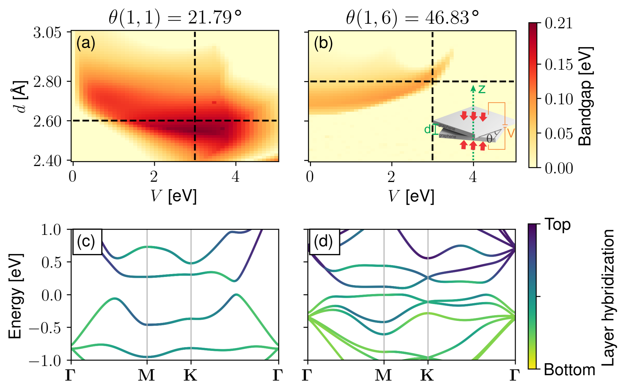
Figures 1(a) and 1(b) show color plots of the single-particle bandgap dependence on the interlayer distance and the applied electric field magnitude for a TBG with twist angle (a) and (b) . Results for different twist angles, corresponding to TBG structures that generate commensurable unit cells of less than atoms, are given in Sec. S3 of the Supplemental Material [41]. Our findings demonstrate, in certain cases, bandgaps up to eV, when one combines electric bias and pressure, although just one of them is enough to generate a gap opening in some cases, as shown in Fig. S3 of the Supplemental Material [41]. Therefore, it turns TBG into a narrow gap semiconductor and, consequently, robust enough to support excitons. The electronic band structures and their layer composition, associated with the spatial localization of the electrons on the individual layers projected in each band, for a fixed bias potential eV are depicted in Figs. 1(c) for an interlayer distance of Å and twist angle of and 1(d) for Å and , revealing strong layer hybridization around the bands’ edges in both cases. Thus, we will show that gapped TBG hosts layered-hybridized moiré excitons. Besides pressure, we could also consider the stretching of TBG layers, not included here, which would increase the interlayer over intralayer hopping ratios, favoring the appearance of a bandgap. Recently, it has been demonstrated [26] that the sliding of one graphene layer over the other could open a bandgap.
Dieletric screening, excitons, and optical response for TBG.— To properly describe electron-hole bound states, the screened interaction should be incorporated in the formalism [46]. For that, we consider the static dielectric function within the RPA and use the Adler-Wiser formula [36, 37] adapted here for 2D system (see Sec. S3 in Supplemental Material [41]), resulting in
| (5) |
where is the reciprocal lattice vector of the superlattice, () is the conduction (valence) band-index, is the surface area of the system, and the overlap term is defined as
| (6) |
being the Bloch wavefunction component of the localized in the site of the supercell. The term is associated with the bare electron-electron interaction, obtained by solving the Poisson equation. It is written as
| (7) |
where and contributions correspond to the intralayer and interlayer interactions, respectively. In the long-wavelength approximation, the dielectric function (Moiré excitons in biased twisted bilayer graphene under pressure) becomes , that corresponds to the Rytova-Keldysh potential with a screening length [47]. Thus, by numerically calculating the dielectric function (Moiré excitons in biased twisted bilayer graphene under pressure) and taking the first-order expansion term (see Sec. S3 and Fig. S4 in Supplemental Material [41]), one gets Å, and Å, for the intralayer contribution in the twist angles of and , respectively, being them higher than the value for monolayer TMDs [48]. The obtained values obey the trend reported in Ref. [49] that the smaller the bandgap, the higher value. The effective interaction, taking into account the screening of pz orbitals of the twisted structure in each layer, is given by
| (8) |
that shows a different screening for interlayer and intralayer potentials (see Sec. S5 in Supplemental Material [41]).
To study the exciton properties using the tight-binding formalism, we employ the Semiconductor Bloch Equations (SBE) [38], as explained in detail in Sec. S5 in Supplemental Material [41]. The SBE is obtained by writing the Heisenberg equation of motion for the interband transition amplitude , with being the annihilator operator for an electron at the band with wavenumber for the incidence of an electromagnetic wave with frequency and amplitude . We neglected the Auger process, considering only the highest valence (v) and lowest conduction bands (c), and used the rotating-wave approximation and equilibrium occupation numbers for . In this case, the SBE read as
| (9) |
where is the renormalized transition energy with the inclusion of the exchange self-energy , is a phenomenological term for the relaxation transition rate, the integral is performed over the first Brillouin zone, is the dipole matrix element, and the Kernel is
| (10) |
with the exchange self-energy read as:
| (11) |
For the calculation of exciton states, we solve the homogeneous version of Eq. (9), setting and to be the corresponding eigenvalue.
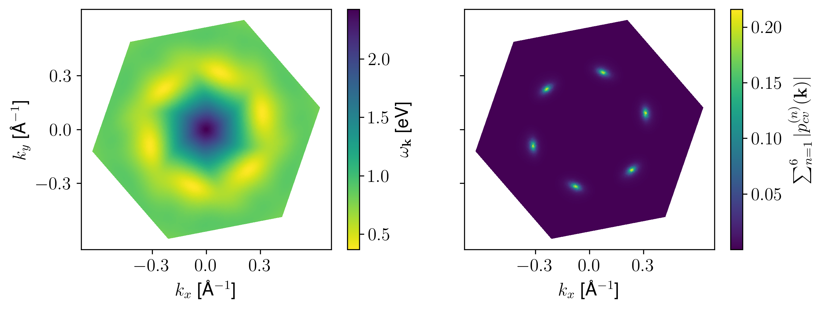
From the numerically calculated Bloch functions and using the inverse of the dielectric function (Moiré excitons in biased twisted bilayer graphene under pressure), we obtain the exchange self-energy term and then the renormalized optical band . Such results are shown in Fig. 2(a) for , eV, and Å and for , eV and Å in Fig. S5(a) in Supplemental Material [41]. For , the renormalization of the bandgap was almost of meV, resulting in bandgaps up to meV; however, no pronounced qualitative changes were observed from the transition energy . From Fig. 2(a), one clearly notices a six-fold minimum in the spectrum located on the band edges along the – path in the first Brillouin zone of the supercell. In Fig. 2(b), we show the superposition of the six first excitonic wavefunctions in momentum space, each of them located exactly at one of the six minima of the optical band. They are also strongly anisotropic, spread along the direction orthogonal to the – path. In Sec. S5 of Supplemental Material [41], we present the layer hybridization’s calculation of the excitonic bound states, showing that both the electrons and holes are highly hybridized between the two layers.
For bright excitons, reflectance and absorption measurements will show signatures of their presence [50]. From the SBE (9), we can compute the optical conductivity and, therefore, the absorption [51]. As we are interested in the frequencies near the exciton resonance, we use Elliot’s formula for the optical conductivity (see Sec. S5 in the Supplemental Material [41])
| (12) |
with being the outer product, , and the dimensionless exciton dipole moment
| (13) |
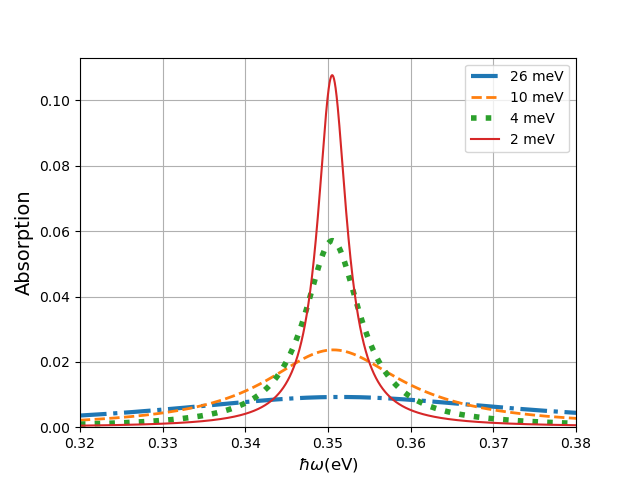
where are the normalized excitonic eigenmodes of the homogeneous version of Eq. (9). From the optical conductivity , we calculate the absorption for a suspended sample, where we include the contribution of the first six degenerated exciton states (see Fig. 2), and we show the results in Fig. 3 for different values of the relaxation rate , that represents the effects of disorder and temperature. The absorption increases as the nonradiative decay rate decreases, reaching values up to 10% absorption for meV; a value that is compatible with excitons in TMDs [52]. Thus, we show that optical measurements can probe the presence of excitons in this system.
Conclusion.—In summary, we demonstrated that a bandgap can be induced in TBG under pressure for realistic conditions when a voltage bias is applied. In this gapped TBG case, we predicted the existence of highly anisotropic moiré excitons that strongly interact with light. Moreover, the methodology developed here for studying excitons in moiré systems can be applied to other 2D twisted materials.
Acknowledgments
V. G. M. D. acknowledges a Msc. scholarship from the Brazilian agency CAPES (Fundação Coordenação de Aperfeiçoamento de Pessoal de Nível Superior). A. J. C., L. K. T, and D. R. C. were supported by CNPq (Conselho Nacional de Desenvolvimento Científico e Tecnológico) Grant No. 400789/2019-0, 310422/2019-1, 308486/2015-3, 310422/2019-1, 315408/2021-9, 423423/2021-5, 408144/2022-0, and 313211/2021-3. N.M.R.P. acknowledges support from the Independent Research Fund Denmark (grant no. 2032-00045B) and the Danish National Research Foundation (Project No. DNRF165). A. J. C. acknowledges Fundação de Amparo à Pesquisa do Estado de São Paulo (FAPESP) under Grant No. 2022/08086-0, and is kindly grateful to INL (International Iberian Nanotechnology Laboratory) for the warm hospitality, where part of this work was carried out.
References
- He et al. [2021] F. He, Y. Zhou, Z. Ye, S.-H. Cho, J. Jeong, X. Meng, and Y. Wang, ACS nano 15, 5944 (2021).
- Rakib et al. [2022] T. Rakib, P. Pochet, E. Ertekin, and H. T. Johnson, Journal of Applied Physics 132, 120901 (2022).
- Johnson and Tyson [1969] D. J. Johnson and C. N. Tyson, Journal of Physics D: Applied Physics 2, 787 (1969).
- Cao et al. [2018a] Y. Cao, V. Fatemi, S. Fang, K. Watanabe, T. Taniguchi, E. Kaxiras, and P. Jarillo-Herrero, Nature 556, 43 (2018a).
- Lisi et al. [2021] S. Lisi, X. Lu, T. Benschop, T. A. de Jong, P. Stepanov, J. R. Duran, F. Margot, I. Cucchi, E. Cappelli, A. Hunter, et al., Nature Physics 17, 189 (2021).
- Utama et al. [2021] M. I. B. Utama, R. J. Koch, K. Lee, N. Leconte, H. Li, S. Zhao, L. Jiang, J. Zhu, K. Watanabe, T. Taniguchi, et al., Nature Physics 17, 184 (2021).
- Cao et al. [2018b] Y. Cao, V. Fatemi, A. Demir, S. Fang, S. L. Tomarken, J. Y. Luo, J. D. Sanchez-Yamagishi, K. Watanabe, T. Taniguchi, E. Kaxiras, R. C. Ashoori, and P. Jarillo-Herrero, Nature 556, 80 (2018b).
- Weston et al. [2022] A. Weston, E. G. Castanon, V. Enaldiev, F. Ferreira, S. Bhattacharjee, S. Xu, H. Corte-León, Z. Wu, N. Clark, A. Summerfield, T. Hashimoto, Y. Gao, W. Wang, M. Hamer, H. Read, L. Fumagalli, A. V. Kretinin, S. J. Haigh, O. Kazakova, A. K. Geim, V. I. Fal’ko, and R. Gorbachev, Nature Nanotechnology 17, 390 (2022).
- Song et al. [2021] T. Song, Q.-C. Sun, E. Anderson, C. Wang, J. Qian, T. Taniguchi, K. Watanabe, M. A. McGuire, R. Stöhr, D. Xiao, T. Cao, J. Wrachtrup, and X. Xu, Science 374, 1140 (2021).
- Xu et al. [2022] Y. Xu, K. Kang, K. Watanabe, T. Taniguchi, K. F. Mak, and J. Shan, Nature Nanotechnology 17, 934 (2022).
- Wu et al. [2017] F. Wu, T. Lovorn, and A. H. MacDonald, Physical Review Letters 118, 147401 (2017).
- Zhang et al. [2017] C. Zhang, C.-P. Chuu, X. Ren, M.-Y. Li, L.-J. Li, C. Jin, M.-Y. Chou, and C.-K. Shih, Science Advances 3, e1601459 (2017).
- Mak et al. [2013] K. F. Mak, K. He, C. Lee, G. H. Lee, J. Hone, T. F. Heinz, and J. Shan, Nature Materials 12, 207 (2013).
- Latini et al. [2015a] S. Latini, T. Olsen, and K. S. Thygesen, Physical Review B 92, 245123 (2015a).
- Tartakovskii [2020] A. Tartakovskii, Nature Reviews Physics 2, 8 (2020).
- Seyler et al. [2019] K. L. Seyler, P. Rivera, H. Yu, N. P. Wilson, E. L. Ray, D. G. Mandrus, J. Yan, W. Yao, and X. Xu, Nature 567, 66 (2019).
- Alexeev et al. [2019] E. M. Alexeev, D. A. Ruiz-Tijerina, M. Danovich, M. J. Hamer, D. J. Terry, P. K. Nayak, S. Ahn, S. Pak, J. Lee, J. I. Sohn, et al., Nature 567, 81 (2019).
- Jin et al. [2019] C. Jin, E. C. Regan, A. Yan, M. Iqbal Bakti Utama, D. Wang, S. Zhao, Y. Qin, S. Yang, Z. Zheng, S. Shi, et al., Nature 567, 76 (2019).
- Tran et al. [2019] K. Tran, G. Moody, F. Wu, X. Lu, J. Choi, K. Kim, A. Rai, D. A. Sanchez, J. Quan, A. Singh, et al., Nature 567, 71 (2019).
- Yu et al. [2017] H. Yu, G.-B. Liu, J. Tang, X. Xu, and W. Yao, Science Advances 3, e1701696 (2017).
- Ciarrocchi et al. [2022] A. Ciarrocchi, F. Tagarelli, A. Avsar, and A. Kis, Nature Reviews Materials 7, 449 (2022).
- Ohta et al. [2006] T. Ohta, A. Bostwick, T. Seyller, K. Horn, and E. Rotenberg, Science 313, 951 (2006).
- Castro et al. [2007] E. V. Castro, K. S. Novoselov, S. V. Morozov, N. M. R. Peres, J. M. B. L. dos Santos, J. Nilsson, F. Guinea, A. K. Geim, and A. H. C. Neto, Physical Review Letters 99, 216802 (2007).
- Zhang et al. [2009] Y. Zhang, T.-T. Tang, C. Girit, Z. Hao, M. C. Martin, A. Zettl, M. F. Crommie, Y. R. Shen, and F. Wang, Nature 459, 820 (2009).
- Guo et al. [2008] Y. Guo, W. Guo, and C. Chen, Applied Physics Letters 92, 243101 (2008).
- Talkington and Mele [2023] S. Talkington and E. J. Mele, Physical Review B 107, L041408 (2023).
- Park and Louie [2010] C.-H. Park and S. G. Louie, Nano letters 10, 426 (2010).
- Cheianov et al. [2012] V. Cheianov, I. Aleiner, and V. Fal’ko, Physical Review Letters 109, 106801 (2012).
- Ju et al. [2017] L. Ju, L. Wang, T. Cao, T. Taniguchi, K. Watanabe, S. G. Louie, F. Rana, J. Park, J. Hone, F. Wang, and P. L. McEuen, Science 358, 907 (2017).
- Henriques et al. [2022] J. C. G. Henriques, I. Epstein, and N. M. R. Peres, Phys. Rev. B 105, 045411 (2022).
- van der Zande et al. [2014] A. M. van der Zande, J. Kunstmann, A. Chernikov, D. A. Chenet, Y. You, X. Zhang, P. Y. Huang, T. C. Berkelbach, L. Wang, F. Zhang, M. S. Hybertsen, D. A. Muller, D. R. Reichman, T. F. Heinz, and J. C. Hone, Nano Letters 14, 3869 (2014).
- Tang et al. [2021] Y. Tang, J. Gu, S. Liu, K. Watanabe, T. Taniguchi, J. Hone, K. F. Mak, and J. Shan, Nature Nanotechnology 16, 52 (2021).
- Bohm and Pines [1951] D. Bohm and D. Pines, Physical Review 82, 625 (1951).
- Pines and Bohm [1952] D. Pines and D. Bohm, Physical Review 85, 338 (1952).
- Bohm and Pines [1953] D. Bohm and D. Pines, Physical Review 92, 609 (1953).
- Adler [1962] S. L. Adler, Physical Review 126, 413 (1962).
- Wiser [1963] N. Wiser, Physical Review 129, 62 (1963).
- Kira and Koch [2011] M. Kira and S. W. Koch, Semiconductor quantum optics (Cambridge University Press, 2011).
- Vanhala and Pollet [2020] T. I. Vanhala and L. Pollet, Physical Review B 102, 035154 (2020).
- Lopes dos Santos et al. [2012] J. M. B. Lopes dos Santos, N. M. R. Peres, and A. H. Castro Neto, Physical Review B 86, 155449 (2012).
- sup [Year] Supplementary material, Supplementary Material (Year), available electronically as supplementary material in the article.
- Zhou et al. [2023] X.-F. Zhou, Y.-W. Liu, C.-Y. Hao, C. Yan, Q. Zheng, Y.-N. Ren, Y.-X. Zhao, K. Watanabe, T. Taniguchi, and L. He, Physical Review B 107, 125410 (2023).
- Slater and Koster [1954] J. C. Slater and G. F. Koster, Physical Review 94, 1498 (1954).
- Moon and Koshino [2013] P. Moon and M. Koshino, Physical Review B 87, 205404 (2013).
- Mirzakhani et al. [2020] M. Mirzakhani, F. M. Peeters, and M. Zarenia, Physical Review B 101, 075413 (2020).
- Latini et al. [2015b] S. Latini, T. Olsen, and K. S. Thygesen, Physical Review B 92, 245123 (2015b).
- Cudazzo et al. [2011] P. Cudazzo, I. V. Tokatly, and A. Rubio, Physical Review B 84, 085406 (2011).
- Pedersen [2016] T. G. Pedersen, Physical Review B 94, 125424 (2016).
- Choi et al. [2015] J.-H. Choi, P. Cui, H. Lan, and Z. Zhang, Physical Review Letters 115, 066403 (2015).
- Li et al. [2014] Y. Li, A. Chernikov, X. Zhang, A. Rigosi, H. M. Hill, A. M. van der Zande, D. A. Chenet, E.-M. Shih, J. Hone, and T. F. Heinz, Physical Review B 90, 205422 (2014).
- Chaves et al. [2017] A. J. Chaves, R. M. Ribeiro, T. Frederico, and N. M. R. Peres, 2D Materials 4, 025086 (2017).
- Epstein et al. [2020] I. Epstein, B. Terrés, A. J. Chaves, V.-V. Pusapati, D. A. Rhodes, B. Frank, V. Zimmermann, Y. Qin, K. Watanabe, T. Taniguchi, H. Giessen, S. Tongay, J. C. Hone, N. M. R. Peres, and F. H. L. Koppens, Nano Letters 20, 3545 (2020).