Mitigation of interfacial dielectric loss in aluminum-on-silicon superconducting qubits
Abstract
We demonstrate aluminum-on-silicon planar transmon qubits with time-averaged energy relaxation times of up to 270 s, corresponding to million, and a highest observed value of 501 s. We use materials analysis techniques and numerical simulations to investigate the dominant sources of energy loss, and devise and demonstrate a strategy towards mitigating them. The mitigation of loss is achieved by reducing the presence of oxide, a known host of defects, near the substrate-metal interface, by growing aluminum films thicker than 300 nm. A loss analysis of coplanar-waveguide resonators shows that the improvement is owing to a reduction of dielectric loss due to two-level system defects. We perform time-of-flight secondary ion mass spectrometry and observe a reduced presence of oxygen at the substrate-metal interface for the thicker films. The correlation between the enhanced performance and the film thickness is due to the tendency of aluminum to grow in columnar structures of parallel grain boundaries, where the size of the grain depends on the film thickness: transmission electron microscopy imaging shows that the thicker film has larger grains and consequently fewer grain boundaries containing oxide near this interface. These conclusions are supported by numerical simulations of the different loss contributions in the device.
I Introduction
Limited qubit coherence is still one of the main challenges for developers of solid-state quantum computing hardware. In the gate model of quantum computation, errors per quantum gate well below a tenth of a percent are required to execute meaningful quantum algorithms—and the lower the errors, the less overhead is needed for error correction and error mitigation.
Superconducting qubits represent a leading platform for quantum computation. Their coherence time improvement, from nanoseconds at their conception to milliseconds today, is nothing less than remarkable Nakamura et al. (1999); Houck et al. (2008); Kjaergaard et al. (2020); Somoroff et al. (2023). Progress has been driven by discoveries and systematic engineering to identify and mitigate the sources of decoherence. This effort has two components: a reduction of the qubits’ sensitivity to noise by development of innovative device design concepts Koch et al. (2007); Sage et al. (2011); Dunsworth et al. (2017); Gordon et al. (2022), and a reduction of the noise itself by engineering of the qubits’ electromagnetic environment Burnett et al. (2019); Gordon et al. (2022), improved fabrication methods Megrant et al. (2012); Nersisyan et al. (2019), and materials science Chang et al. (2013); Dunsworth et al. (2017); Murray (2021).
Coplanar-waveguide (CPW) resonators and transmon qubits are commonly used for studying coherence and identifying loss mechanisms in superconducting devices. The dominating decoherence source within these devices is dielectric loss and noise, attributed to charged two-level-system (TLS) defects at surfaces and interfaces, i.e., in thin sheets at the substrate-metal (SM), metal-air (MA), and substrate-air (SA) interfaces Martinis et al. (2005); Macha et al. (2010); Lisenfeld et al. (2019); Molina-Ruiz et al. (2021); Niepce et al. (2021); Osman et al. (2023). Oxide-based defects are known contributors to TLS loss Lisenfeld et al. (2015); Müller et al. (2015).
Among superconducting materials for qubits, aluminum (Al) has been a dominant material within the community: the ease and reproducibility of thin-film deposition, low cost, well-described chemistry, and the robust Josephson effect in small tunnel junctions comprised of aluminum oxide sandwiched between aluminum electrodes have made this material an attractive choice.
The achieved energy relaxation time () of transmon qubits in a planar geometry whose wiring layer is made of aluminum is currently about Dunsworth et al. (2017). However, recent years have seen an impressive improvement for transmon qubits with wiring layers made of tantalum, a less explored material for quantum devices, showing average in the range of 300 – Place et al. (2021); Wang et al. (2022). This progress has subsequently spread to the more traditionally used materials titanium nitride and niobium, with average up to and s, respectively Deng et al. (2023); Kono et al. (2023). An apparent advantage of these materials over aluminum is their ability to withstand harsh chemical surface cleaning.
Here we demonstrate planar transmon qubits made of aluminum on silicon substrates, with time-averaged of up to s ( million, : qubit frequency). The improvement is mirrored in CPW resonators’ quality factor measurements: the Q factor’s dependence on circulating power indicates that the increased relaxation time is due to a reduction of TLS losses. We achieve this improvement by depositing a thicker layer of aluminum—300 nm or more—compared to our previous standard of 150 nm. We conduct material depth profiling by time-of-flight secondary ion mass spectrometry (ToF-SIMS) and identify an aluminum-film-thickness dependence of the oxygen concentration at the SM interface, which decreases for thicker films. Further, we show by transmission-electron microscopy (TEM) that the thicker film has larger grains; we therefore interpret the reduced oxygen presence as being due to a smaller prevalence of grain boundaries in the thicker film and hence fewer sources of interfacial dielectric loss. Our numerical simulations of the loss participation due to the different dielectrics present in the device support this interpretation.
II Qubit coherence
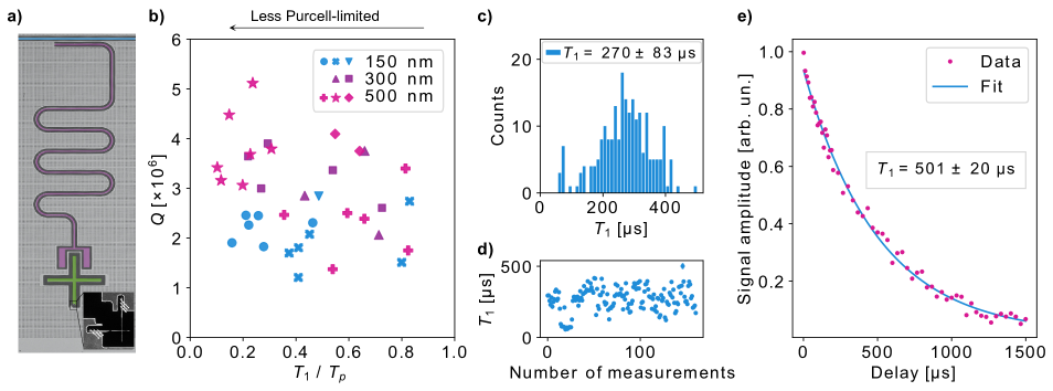
We show a representative schematic of the transmon (Xmon) qubit circuit in figure 1(a). The device has a 2D architecture and consists of a Josephson junction shunted by a large capacitor, which is coupled to a quarter-wavelength (/4) CPW resonator. The CPW resonator is used for readout as well as qubit control. The devices are fabricated on silicon (Si) substrates and stripped of surface oxides prior to Al deposition. We present more details on device fabrication and measurement in sections A and B, respectively.
In figure 1(b), we present coherence data of 36 out of the 38 measured qubits made with Al films of various thicknesses of (previously our standard thickness), , and . Two qubits were disregarded from the analysis due to inconsistent measurement results, see section C. The figure shows a trend towards higher coherence times with thicker films. The average quality factor is for the qubits on the thick film, and for those on the thicker films.
The qubit frequencies range from to , while the resonator frequencies are between and , see table 2. For simplicity of device design and characterization, there is no Purcell filtering present in the device to mitigate spontaneous emission from the qubit into its resonator and the transmission line. Therefore, for these long- qubits, Purcell decay is non-negligible and needs to be included among the limiting factors of the qubits’ lifetime
| (1) |
Here , , , and are the theoretical quality factors attributed to TLS, Purcell decay, quasiparticles, and other radiation losses not related to Purcell decay, respectively.
The time constant of the Purcell decay for each qubit is calculated as , with the decay rate Koch et al. (2007),
| (2) |
where the cavity decay rate is , the qubit-resonator coupling is , and the qubit-resonator detuning is . Here denotes the resonator frequency, represents the resonator’s loaded (total) quality factor and is the dispersive frequency shift.
The qubit-resonator detunings vary between the devices due to variation in the Josephson junctions. Qubits with a smaller qubit-resonator detuning are more strongly Purcell-limited than others. As a result, a direct comparison between the qubits based solely on their is not the correct way of evaluating the qubits’ performance.
To compare qubits of different frequencies while simultaneously taking the effect of the Purcell decay into account, we plot the qubits’ quality factor as a function of in figure 1(b). We choose instead of since the latter depends directly on frequency, which also varies across devices. Now, rewriting Equation (1) while ignoring the loss due to quasiparticles and radiation, we are left with . The quality factor will therefore approach its limit set by the TLS loss when .
In figure 1(b), the data shown in blue belong to qubits fabricated on a thick wiring layer, while the purple and pink markers show qubits fabricated on 300 and thick layers, respectively. While the average for the thicker films is higher, the separation between the datasets scales with the Purcell effect. When , a range at which the qubits are not significantly limited by Purcell decay, the data for the thicker and thinner films are clearly separated, with the qubits fabricated with the thinner film () showing a lower quality factor compared with those on the thicker films ( ). There is a subtle difference between the quality factors of the qubits on 300 and films; however, the difference is not so pronounced as to clearly differentiate the qubits with these two film thicknesses. The average quality factor in this range is for the qubits on the thin film, while it increases by 66 % to for those on the thicker films. For a more stringent case of , the average quality factor becomes for the thicker films. Assuming a typical qubit frequency of = , the corresponding relaxation time becomes for a qubit made from the thicker 300 - films, in the weakly Purcell-limited regime.
We remark that the coherence times quoted in figure 1(b) are mean values gathered by measuring each qubit for at least . This is necessary to accurately assess a qubit’s quality, since the coherence time of superconducting qubits is known to fluctuate over time Chang et al. (2013); Müller et al. (2015); Burnett et al. (2019); Schlör et al. (2019). In figure 1(c) we show the histogram of the relaxation time of the best qubit, labeled Q27 in table 2. The histogram contains 160 averaged values (see figure 1(d)) obtained over a span of . We find an average relaxation time of , on par with the numbers reported for the best qubits on titanium nitride and niobium films Kono et al. (2023); Deng et al. (2023). In figure 1(e) we present the longest measured relaxation time for the aforementioned qubit, together with its corresponding fit, showing .
The improvement of the relaxation time in the thicker films is also reflected in the values obtained for the spin echo decoherence time , as for most of our qubits, see table 2. Although we find mean values as long as , the spin echo decoherence time does not quite reach the theoretical maximum of , indicating that the coherence of our qubits is not solely limited by , or by the type of dephasing noise typically cancelled by the spin echo sequence.
III Resonator quality
In order to distinguish and quantify the particular energy loss mechanisms at play, we also fabricate and measure 50 bare /4 CPW resonators with resonance frequencies in the range of 4 – . The internal quality factors of the resonators are extracted by fitting the transmission scattering parameter vs. frequency using a resonance circle fitting method with diameter correction adapted directly from Probst et al. (2015).
For TLS-loss-limited resonators, at low drive powers will be diminished according to the model for interacting TLSs Gao (2008); Pappas et al. (2011); Goetz et al. (2016),
| (3) |
where describes the loss due to parasitic TLSs, with quantifying the TLS filling (also known as the total TLS participation ratio), and the TLS density. is the critical photon number required to saturate a single TLS on average, and describes how quickly the TLSs saturate with power. The temperature-dependent factor is 1 in our temperature regime ( denotes the temperature, and and are the Planck and Boltzmann constants, respectively). The power-independent term quantifies other sources of loss, such as resistive or radiative losses. The average number of photons circulating in the resonator is estimated using
| (4) |
where and are the characteristic impedances of the transmission line and the resonator, respectively, and is the microwave power delivered to the input port of the device. and are the loaded and coupling quality factors, respectively.
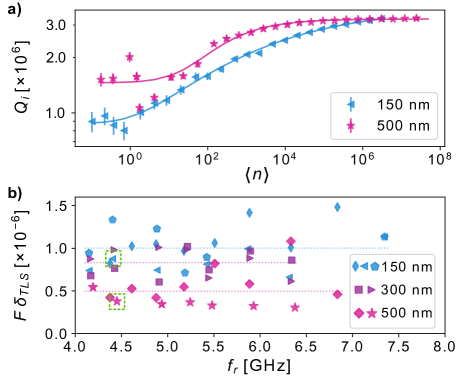
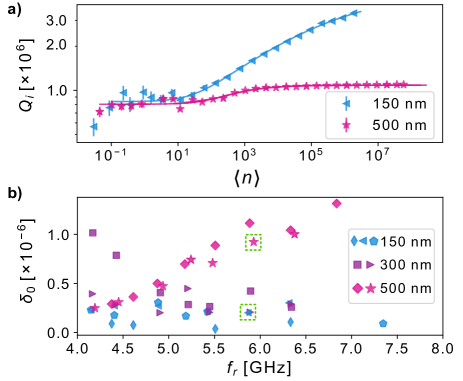
In figure 2(a), we compare the extracted of two resonators with the same resonance frequency ( ) on 150 and films. Both resonators show a similar when . However, the resonator fabricated on the film has a higher internal quality factor at lower photon levels. We fit the quality factors to the TLS model of Equation 3 and obtain , presented in figure 2(b) for all of the resonators. For the resonators on the film, has settled at a lower level ( on average) in comparison with those made with the film ( on average), indicating a reduction in the loss due to the TLSs. As for the resonators made with the Al, is in-between, with an average value of .
From the fit we also obtain in Equation 3, see figure 7 in section D. Interestingly, we observe a frequency-dependent increase in the non-TLS related loss, , in the thick films. We did not observe this increased loss in our qubits, whose frequencies lie below , where this loss seems to be less prominent. However, depending on its origin as well as its dependence on device geometry, this loss mechanism could become limiting for higher-frequency qubits fabricated on thicker films. We present a further investigation of this loss in section D.
In the model for interacting TLSs, the parameter describes how sharply the TLSs saturate with increased power. In our data, is scattered, falling between 0.15 - 0.4 for most resonators (which is typically reported in studies Burnett et al. (2017)), with no discernible trend across the devices.
IV Materials analysis
The presence of parasitic TLS defects is mainly attributed to amorphous oxides at the materials interfaces Martinis et al. (2005); Lisenfeld et al. (2015), although their microscopic origin is debated. We therefore perform an elemental analysis of representative samples, focusing on oxygen (O) residing near the material interfaces. We perform this analysis using time-of-flight secondary ion mass spectrometry (ToF-SIMS), a highly accurate method capable of simultaneous analysis of species with different masses Benninghoven (1994). To obtain a depth profile of the species of interest across all interfaces, we use an auxiliary sputter beam. This method is further detailed in section E.
The samples under analysis are pieces of a Si wafer coated with Al films of the three different thicknesses representative of our devices (150, 300, and ). To discount wafer-to-wafer variation in substrate material properties, these three pieces originate from the same wafer. After the splitting of the wafer, the Si pieces underwent a cleaning and deposition procedure identical to that used during the qubit and resonator fabrication.
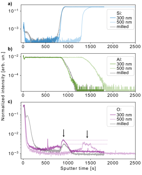
The intensity of the detected signal identifying Si, Al, and O across the thickness of the sample is plotted in figure 3, normalized to the total ion count. Each trace starts at the metal-air (MA) interface, then continues through the metal, and ends inside the substrate.
In figure 3(a), we detect Si at the MA interface, which is likely coming from ambient air. Sputtering away more material of the stack, the intensity of Si is low inside the metal, then rises abruptly at the SM interface, and saturates inside the Si substrate. In figure 3(b), the intensity of the Al signal is initially high at the MA interface and inside the Al film, then plummets to the detection limit once we reach the substrate.
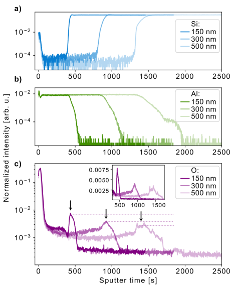
In figure 3(c), the intensity of the O signal starts high at the aluminum oxide-passivated MA surface, then stabilizes at a lower level inside the film. Sputtering further, there is a peak in the O intensity at the SM interface, after which the trace levels out inside the Si substrate.
The diffusion constant of oxygen in aluminum is low at room temperature Ross et al. (2017); however, diffusion along grain boundaries is substantially faster Jaseliunaite and Galdikas (2020). Oxygen can exist in aluminum along the grain boundaries, as the evaporated Al grows in high vacuum with a tendency to follow a columnar growth structure Adamik et al. (1998). This observation emphasizes that lossy oxides exist not only at the direct interfaces, but also within the grainy metal films, contributing to dielectric loss when in the vicinity of the interfaces.
We suggest that the peak at the SM originates from both the continuation of oxide along the grains, as well as from an interfacial oxide. The origin of this interfacial oxide could be a result of incomplete silicon oxide removal, or oxide regrowth after removal during transfer to the evaporator or while inside, resulting from residual oxygen content of the evaporation chamber. In section E we show that the oxygen is mainly present in the form of aluminum oxide, which is consistent with the thermodynamically favorable reduction of silicon oxides into aluminum oxides Dadabhai et al. (1996); Goodnick et al. (1981).
Comparing the three films in figure 3(c), we find that the oxygen level inside the film decreases in the thicker films. The peak intensity is also lower in the thicker films, as indicated with the dashed lines.
While it appears in the data as if the Si/Al interface were broadening with increasing film thickness, this is unlikely to be a real feature of the samples. Instead, this broadening is a known artifact caused by surface roughening and atomic mixing during the sputter-assisted depth profiling Yan et al. (2019); Gorbenko et al. (2016). Although disregarding the width of the peaks in similar scenarios is not unusual, we compare both the peak intensity and the integrated intensity for O across the entire Al film. We find a similar trend in both cases, that the intensity of the oxygen signal is strongest for the thinnest film. At the SM interface, the O intensity peak level scales with the ratio of 5:3:2 for , , and films, respectively. The integrated intensity for O across the entire Al film, including the MA and SM interfaces, divided by film thickness scales with a ratio of 6:3:2.
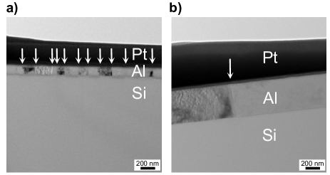
Increasing a film’s thickness has a direct effect on the resulting grain size Chaverri et al. (1991); Nik et al. (2016), which we confirm using transmission electron microscopy (TEM). In figure 4, we observe long vertical grain boundaries which stretch uninterrupted all the way from the top surface to the interface with the Si substrate. The grain size increases with film thickness, which strongly impacts the morphology of the material interfaces. A larger grain size also provides fewer grain boundaries to trap residual oxygen during deposition, as well as to act as diffusion channels upon contact with ambient atmosphere. While the electric field well inside the superconducting film is low, and therefore grain boundaries inside the film are unlikely to lead to additional loss, fewer grain boundaries acting as hosts of TLS in the vicinity of the SM interface can decrease the dielectric loss of this interface. Since the contribution of the SM interface to the overall loss is substantial (see section V), a small change in the concentration of potential TLS defects has a significant impact on the total loss in the circuit.
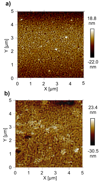
At the MA interface, the oxygen contribution from the surface oxide is considerably greater than the oxide along the grain boundaries. As such, we do not observe a tangible effect in the reduction of oxygen presence between the samples with different densities of grain boundaries. The measurement traces identifying oxygen species at the surface of the three different film thicknesses are indistinguishable. Altering the thickness of a thin film can affect the MA interface as well, by way of changing the roughness of the film’s top surface. We perform an atomic force microscopy (AFM) to evaluate the surface roughness of a and a film, obtaining root mean square roughness values of and , respectively, over a area (figure 11). This negligible difference, in conjunction with no observed change in MA oxide in the SIMS measurement, further discounts this interface from explaining the coherence measurement data.
V Participation ratio simulations
In this section, we present energy participation ratio simulations of a 2D CPW geometry, showing that the reduced loss at the SM interface is the most likely reason for the improved quality factors of the devices made with thicker aluminum films. We also investigate if and when the loss due to other interfaces becomes dominant.
| Interface | Thickness | Thickness | ||
|---|---|---|---|---|
| Fig 5(b) | Fig 5(c) | |||
| Al | - | - | 50 - | |
| Air | 0 | 1.0 | ||
| Si | 11.7 | |||
| MA | 7.0 | |||
| SA | 4.0 | |||
| SM | 4.0 | 0.4 - | ||
| corner | 4.0 |
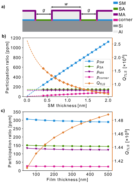
The cross section of the simulated device is illustrated in figure 5(a), with the center conductor width and the gap to ground , which corresponds to a impedance. Using the material parameters in table 1 Martinis and Megrant (2014); Wang et al. (2015), we first sweep the thickness of the dielectric at the SM interface and obtain the participation ratios presented in figure 5(b). The data points show the simulation results from down to , while the lines represent polynomial fits to estimate the participation ratios for a thinner dielectric. The total loss due to TLSs, i.e., – with presented in figure 5(b) as well – scales with the participation ratio weighted by the loss tangent of the material
| (5) |
where and denote the participation ratio and the loss tangent at interface , respectively (: Si, MA, SA, SM and corner). The various interfaces are illustrated in figure 5(a).
The energy participation ratio at the MA and SA interfaces changes negligibly by varying the dielectric thickness at the SM. However, at the SM interface (and the corresponding corners), there is a linear dependence of the field concentration on the SM dielectric thickness. Moreover, compared to the MA and SA interfaces, a considerable fraction of the electric field resides at the SM interface. With the removal of the silicon native oxide prior to metal deposition, the effective dielectric thickness at the SM interface is estimated to be about Kosen et al. (2022). The resulting participation ratio, and the corresponding loss, assuming equal loss tangents, is about twice those at the MA and SA interfaces. Reducing the SM dielectric to about decreases the corresponding SM loss, yielding an almost equal value of the participation ratio by the three interfaces. Below this level, the loss is dominated by the MA and SA interfaces.
We ran a second round of simulations to explore the evolution of participation ratios if the thickness of the metallic layer is varied. The presented results in figure 5(c) show only a slight variation in the participation ratios, as well as in the quality factor of the resonator. From the simulations above and the materials analysis in section IV, we conclude that the better performance of the devices with the thicker metallic layers is due to the reduction of the dielectric loss at the SM interface, by way of reducing the number of grain boundaries.
VI Conclusion
We observe a significant improvement in the energy relaxation time of transmon qubits on silicon substrates when fabricated using aluminum films thicker than , whereas the previous standard in our laboratory, and generally in the field, has been thinner. This observation is based on measurements of 36 qubits and 50 resonators. We demonstrate transmon qubits with average relaxation times exceeding on films, with the best qubit showing a time-averaged , corresponding to .
Despite removing the native oxide of the silicon substrate prior to Al deposition, we detect a presence of oxygen and aluminum oxide at the Al–Si interface, which, due to the relatively strong electric field at this interface, contributes to dielectric loss. Material-depth characterization by ToF-SIMS reveals a weakening intensity of the oxygen-signal peak at the substrate-metal interface with increasing film thickness from 150 to 300 to .
We attribute the lower intensity of oxygen at the SM interface of thicker films, hence their lower dielectric loss, to the increased grain size in the thicker film, which we confirm in a TEM analysis. This consequently reduces the prevalence of oxidized grain boundaries in the vicinity of the interface, leading to lower loss.
From a study of loss in CPW resonators, we conclude that the contribution from TLS defects decreases for the thicker films and becomes comparable to loss due to other mechanisms. Whether growing even thicker films—or indeed using epitaxial films—can deliver qubits of superior performance demands further investigations. Our experiments and simulations point towards two obstacles: Firstly, a frequency-dependent loss appears for the thickest film of . Secondly, with the reduced dielectric thickness at the SM interface (below about ), the corresponding interfacial loss falls below that of the other interfaces, with a lower impact on the total loss.
Acknowledgements.
We are grateful for discussions with Liangyu Chen, Simone Gasparinetti, Stefan Gustafsson, Lars Jönsson, Mikael Kervinen, Zeinab Khosravizadeh, Sandoko Kosen, Sergey Kubatkin, David Niepce, Andreas Nylander, Eva Olsson, Marco Scigliuzzo, Daryoush Shiri, Giovanna Tancredi and Lunjie Zeng. The device fabrication was performed at Myfab Chalmers. The ToF-SIMS measurements were performed at the Chemical Imaging infrastructure at Chalmers University of Technology. The TEM was performed at the Chalmers Materials Analysis Laboratory. This work was funded by the Knut and Alice Wallenberg (KAW) Foundation through the Wallenberg Center for Quantum Technology (WACQT), and by the EU Flagship on Quantum Technology HORIZON-CL4-2022-QUANTUM-01-SGA project 101113946 OpenSuperQPlus100.Appendix A Device design and fabrication
In figure 1 we show a representative qubit design. It consists of a Josephson junction shunted by a large cross-type capacitor, which is coupled capacitively to the open end of a quarter-wavelength (/4) CPW resonator. This resonator is in turn inductively coupled via the shorted end to the input/output transmission line.
For readout resonators, both the center conductor width and the gap to the ground are , while for the qubit capacitor . The device structures are surrounded by an array of flux-trapping holes Chiaro et al. (2016). These are squares with a long side, and a pitch. The bare resonators used for energy loss quantification are also of the /4 CPW type, with , coupled capacitively to the transmission line.
The devices are fabricated on high-resistivity () intrinsic silicon substrates. The substrates are stripped of their native oxide in a 2% aqueous solution of HF and subsequently rinsed with deionized water to leave the Si surface terminated with a hydrogen monolayer Trucks et al. (1990).
Immediately after rinsing, we load the Si wafer into the load-lock of a Plassys MEB 550s evaporator, where it is heated to for and then left to cool down to room temperature. This is done to desorb impurities and moisture from the surface of the wafer, and to allow the evaporator to reach a satisfactory vacuum level of in the evaporation chamber. We deposit the aluminum films at the rate of , and then oxidize the top surface in situ in the load-lock without breaking the vacuum, in a static oxidation step.
We then define all circuitry barring the Josephson junctions (JJs) in an optical lithography step. This includes the transmission line, the coplanar waveguide (CPW) resonators, qubit capacitors, and flux trapping holes. We use a resist stack of an e-beam resist, PMMA A2, and an optically sensitive resist such as S1805. The PMMA layer underneath the optical resist serves to protect the underlying Al from damage induced by the TMAH present in the photo-developer (MF319), which enables re-patterning. After successful patterning, the PMMA is ashed away in oxygen plasma. The pattern defined in the resist stack is then transferred into the Al layer via wet etching in a mixture of phosphoric, nitric, and acetic acids (aluminum etchant type A).
For qubit devices, JJs are fabricated using the patch-integrated cross-type technique adapted from Osman et al. (2021). The JJ electrodes pattern is transferred to the MMA EL12 + PMMA A6 resist stack using e-beam lithography (EBL), followed by deposition of the electrodes’ metal in the Plassys evaporator using shadow evaporation and planetary turn. The thickness of the bottom electrode is and the top electrode is thick. A liftoff in Remover 1165 completes the fabrication.
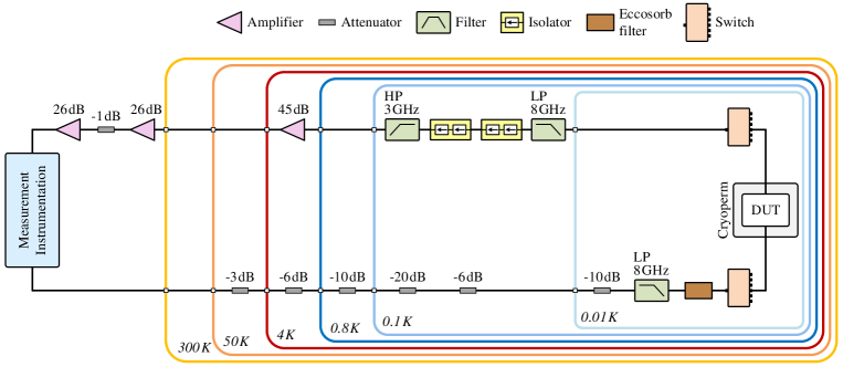
Appendix B Measurement setup
We perform all of the microwave measurements at . The devices under test are placed in a light-tight copper sample box, mounted on a copper tail attached to the mixing chamber stage of a Bluefors LD250 dilution refrigerator. The copper tail is enclosed by a copper can coated with a layer of Stycast mixed with carbon and silicon carbide on the inside, which is in turn enclosed by a Cryoperm magnetic shield.
Figure 6 shows the cryogenic measurement setup with all components including attenuators, filters, microwave switches, isolators and amplifiers. Apart from the attenuators marked in the diagram, the input line itself attenuates by an additional , as determined from an ac-Stark shift measurement C. S. Macklin (2015); Bruno et al. (2015).
As for the room temperature instrumentation, all resonator spectroscopy measurements necessary for the factor extraction are performed using a R&S ZNB8 vector network analyzer (VNA). When necessary, additional attenuation up to is placed at the VNA output, in order to reach powers equivalent to a single photon circulating in the resonators.
The qubits are characterized using two alternative measurement setups. One setup consists of a multi-frequency lock-in amplifier platform (Intermodulation Products Presto-16), where both the pulses necessary to control the qubit and read out its resonator are synthesized directly on an FPGA. The measured signal is also digitized on this FPGA. The alternative qubit measurement setup consists of high frequency signal generators (R&S SGS100a) and arbitrary waveform generators (Keysight PXIe M3202A 1GS/s AWG), whose outputs are upconverted with the help of local oscillators to generate the desired high frequency pulses. The detected signal is digitized using a Keysight PXIe M3102A 500 MS/s digitizer. Both setups have been verified to yield identical coherence results.
Appendix C Summary of qubit measurements
We measured 38 qubits fabricated on 8 separate wafers. The key parameters such as the aluminum film thickness, qubit frequency , readout resonator frequency , the qubit-resonator detuning , the arithmetic mean values (plus/minus one standard deviation) for the relaxation time and the spin echo decoherence time , the qubit quality factor , and the calculated Purcell-decay time , are summarized in table 2.
Two qubits with possibly inaccurately obtained parameters are not included in the analysis in figure 1. These are Q22 () and Q38 (). This could be due to parameter fluctuations during the measurement time span.
For Q38, the measured exceeded the inferred from the device parameters. This is possibly due to the asymmetry of the resonance dip caused by an impedance mismatch. This gives the qubit some protection from decay, which is not accounted for in the model used for the Purcell decay calculations.
| Thickness | |||||||||
|---|---|---|---|---|---|---|---|---|---|
| (nm) | (GHz) | (GHz) | (GHz) | ||||||
| Q1 | 150 | 4.711 | 6.035 | 1.324 | 51 9 | 79 17 | 64 | 1.5 | |
| Q2 | 150 | 4.662 | 6.173 | 1.511 | 58 14 | 100 25 | 155 | 1.7 | |
| Q3 | 150 | 4.923 | 6.317 | 1.394 | 39 6 | 66 11 | 95 | 1.2 | |
| Q4 | 150 | 4.721 | 6.039 | 1.318 | 70 11 | 110 30 | 155 | 2.1 | |
| Q5 | 150 | 4.634 | 6.175 | 1.541 | 62 18 | 101 37 | 151 | 1.8 | |
| Q6 | 150 | 4.449 | 6.320 | 1.871 | 98 27 | 135 46 | 118 | 2.7 | |
| Q7 | 150 | 3.650 | 6.036 | 2.386 | 124 33 | - | 255 | 2.8 | |
| Q8 | 150 | 4.689 | 6.401 | 1.712 | 62 13 | - | 223 | 1.8 | |
| Q9 | 150 | 4.388 | 6.036 | 1.648 | 82 17 | - | 370 | 2.3 | |
| Q10 | 150 | 4.251 | 6.102 | 1.851 | 92 28 | - | 436 | 2.5 | |
| Q11 | 150 | 4.126 | 6.259 | 2.133 | 89 25 | - | 192 | 2.3 | |
| Q12 | 150 | 3.939 | 6.097 | 2.158 | 99 28 | - | 384 | 2.5 | |
| Q13 | 150 | 3.742 | 6.254 | 2.512 | 81 30 | - | 512 | 1.9 | |
| Q14 | 300 | 4.510 | 6.075 | 1.564 | 92 28 | 106 26 | 127 | 2.6 | |
| Q15 | 300 | 4.221 | 6.212 | 1.991 | 113 23 | 135 22 | 421 | 3.0 | |
| Q16 | 300 | 3.883 | 6.355 | 2.473 | 160 39 | 175 30 | 545 | 3.9 | |
| Q17 | 300 | 4.027 | 6.070 | 2.043 | 133 18 | 101 14 | 247 | 3.4 | |
| Q18 | 300 | 3.692 | 6.350 | 2.658 | 157 40 | 228 71 | 716 | 3.6 | |
| Q19 | 300 | 4.899 | 6.072 | 1.173 | 67 15 | 61 15 | 94 | 2.1 | |
| Q20 | 300 | 4.490 | 6.209 | 1.719 | 133 25 | 116 21 | 202 | 3.8 | |
| Q21 | 300 | 4.283 | 6.352 | 2.069 | 106 17 | 146 24 | 245 | 2.9 | |
| Q22 | 500 | 4.729 | 6.113 | 1.384 | 64 18 | 158 58 | 108 | 1.9 | |
| Q23 | 500 | 4.421 | 6.251 | 1.830 | 135 33 | 159 56 | 211 | 3.8 | |
| Q24 | 500 | 4.176 | 6.396 | 2.220 | 156 43 | 165 54 | 285 | 4.1 | |
| Q25 | 500 | 2.873 | 6.250 | 3.377 | 248 109 | 216 90 | 1678 | 4.5 | |
| Q26 | 500 | 3.164 | 6.393 | 3.229 | 159 44 | 9 1 | 1360 | 3.2 | |
| Q27 | 500 | 3.016 | 6.386 | 3.371 | 270 83 | 307 114 | 1141 | 5.1 | |
| Q28 | 500 | 3.206 | 6.108 | 2.902 | 152 31 | 196 33 | 766 | 3.1 | |
| Q29 | 500 | 3.490 | 6.246 | 2.756 | 168 31 | 248 48 | 739 | 3.7 | |
| Q30 | 500 | 2.776 | 6.244 | 3.468 | 196 39 | 177 39 | 1909 | 3.4 | |
| Q31 | 500 | 3.895 | 6.390 | 2.495 | 155 52 | 252 80 | 505 | 3.8 | |
| Q32 | 500 | 4.641 | 6.304 | 1.663 | 60 19 | 90 30 | 73 | 1.7 | |
| Q33 | 500 | 4.810 | 6.577 | 1.767 | 79 14 | 99 19 | 120 | 2.4 | |
| Q34 | 500 | 4.672 | 6.440 | 1.768 | 84 22 | 143 50 | 236 | 2.5 | |
| Q35 | 500 | 4.798 | 6.722 | 1.924 | 83 21 | 110 27 | 140 | 2.5 | |
| Q36 | 500 | 4.750 | 6.303 | 1.553 | 46 13 | 75 23 | 85 | 1.4 | |
| Q37 | 500 | 4.830 | 6.441 | 1.611 | 112 30 | 151 39 | 138 | 3.4 | |
| Q38 | 500 | 5.025 | 6.578 | 1.553 | 77 13 | 122 26 | 61 | 2.4 |
Appendix D High-power loss of thicker films
In section III we observe that TLS-related loss, which shows itself in the suppressed of CPW resonators when the average circulating photon number is low, is mitigated in thicker aluminum films. However, we also observe that the energy loss due to other mechanisms, which imposes an upper limit for at high , increases for the CPWs fabricated on thick films. Similarly to TLS loss, we quantify these other losses by fitting the experimental data to Equation 3. The extracted parameter representing non-TLS-related losses is shown in figure 7. At high frequencies, this loss becomes a limiting factor of the resonators made on thicker films.
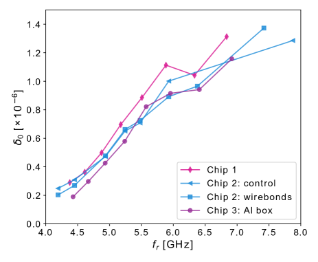
To find the source of the frequency-dependent loss, in Equation 3, we measure resonators fabricated on the thick, Al film, under different scenarios. The first two chips labeled with Chip 1 and Chip 2 in figure 8 are the control chips whose results are presented in figure 7, as well. After the measurement, we wire-bonded across the main transmission line and the resonators on Chip 2 in order to suppress parasitic slotline modes Abuwasib et al. (2013); Chen et al. (2014). In addition, we placed another chip in an aluminum sample box instead of the usual copper box (Chip 3). We expected this to change the coupling between the resonators and the box mode, resulting in a different radiation into the box mode. We did not observe any noticeable difference in the obtained, from which we conclude that, at the moment, neither of these two (the slotline modes or radiation into the box mode) are limiting the coherence of our devices.
Appendix E Additional materials analysis
In ToF-SIMS, a primary focused ion beam is used to sputter elements away from the sample surface. The secondary ions ejected during sputtering are accelerated towards a mass spectrometer, where their time-of-flight and mass/charge ratios are analyzed.
In our measurements we are interested in a depth profile of the various elements across the Si/Al material stack. Therefore, we use an auxiliary 3 keV Cs+ sputter beam with a raster size of in conjunction with the primary 25 keV Bi3+ ion beam used for the secondary ion detection. The raster area of the primary Bi3+ ion beam is . The Cs dose density at 2500 sputter seconds was ions/cm2. To reduce the signal from residual gases in the chamber in the depth profile, the analysis is performed in high vacuum in the range of 2.6 – .
We study the distribution of the detected oxygen between silicon and aluminum oxides at the Si/Al interface in figure 9. The presence of silicon oxides is very low, barely above the detection limit. On the other hand, the presence of aluminum oxide is substantial.
In an Si/\ceSiO2/Al interface, it is thermodynamically favourable for Al to reduce \ceSiO2 and form \ceAl2O3 instead Bauer et al. (1980); Zeng et al. (2013):
| (6) |
We notice also a considerable presence of SiOx at the top surface of the metal. The source of this is likely atmospheric.
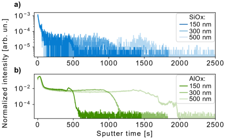
In addition, we analyze a sample where a 500 nm thick film was initially deposited, and later reduced down to 300 nm via argon ion milling. This is done to draw a comparison between this sample and the films of the two respective thicknesses, and trace the origin of the change in interfacial composition. These measurements were performed at 9.1 – . We present the obtained intensity traces for Si, Al and O for two samples of the representative thicknesses ( and , same samples as figure 3), as well as the sample reduced from to , in figure 10.
Figure 10(c) shows the O intensity. At the MA interface, the milled sample shows a higher O content in the top layers, likely due to damage during milling. At the SM interface, the milled sample does not suffer as strongly from decreased depth resolution as the 500 nm thick film, confirming that the SM peak broadening we see in thicker films is indeed a measurement artifact. On the other hand, the milled film retains a comparably low oxygen level at the SM interface as the film.
References
- Nakamura et al. (1999) Y. Nakamura, Y. A. Pashkin, and J. S. Tsai, “Coherent control of macroscopic quantum states in a single-Cooper-pair box,” Nature 398, 786–788 (1999).
- Houck et al. (2008) A. A. Houck, J. A. Schreier, B. R. Johnson, J. M. Chow, J. Koch, J. M. Gambetta, D. I. Schuster, L. Frunzio, M. H. Devoret, S. M. Girvin, and R. J. Schoelkopf, “Controlling the spontaneous emission of a superconducting transmon qubit,” Phys. Rev. Lett. 101, 080502 (2008).
- Kjaergaard et al. (2020) M. Kjaergaard, M. E. Schwartz, J. Braumüller, P. Krantz, J. I.-J. Wang, S. Gustavsson, and W. D. Oliver, “Superconducting Qubits: Current State of Play,” Annu. Rev. Condens. Matter Phys. 11, 369–395 (2020).
- Somoroff et al. (2023) A. Somoroff, Q. Ficheux, R. A. Mencia, H. Xiong, R. Kuzmin, and V. E. Manucharyan, “Millisecond Coherence in a Superconducting Qubit,” Phys. Rev. Lett. 130, 267001 (2023).
- Koch et al. (2007) J. Koch, T. M. Yu, J. Gambetta, A. A. Houck, D. I. Schuster, J. Majer, A. Blais, M. H. Devoret, S. M. Girvin, and R. J. Schoelkopf, “Charge-insensitive qubit design derived from the cooper pair box,” Phys. Rev. A 76, 042319 (2007).
- Sage et al. (2011) J. M. Sage, V. Bolkhovsky, W. D. Oliver, B. Turek, and P. B. Welander, “Study of loss in superconducting coplanar waveguide resonators,” Journal of Applied Physics 109, 063915 (2011).
- Dunsworth et al. (2017) A. Dunsworth, A. Megrant, C. Quintana, Z. Chen, R. Barends, B. Burkett, B. Foxen, Y. Chen, B. Chiaro, A. Fowler, R. Graff, E. Jeffrey, J. Kelly, E. Lucero, J. Y. Mutus, M. Neeley, C. Neill, P. Roushan, D. Sank, A. Vainsencher, J. Wenner, T. C. White, and J. M. Martinis, “Characterization and reduction of capacitive loss induced by sub-micron josephson junction fabrication in superconducting qubits,” Appl. Phys. Lett. 111, 022601 (2017).
- Gordon et al. (2022) R. T. Gordon, C. E. Murray, C. Kurter, M. Sandberg, S. A. Hall, K. Balakrishnan, R. Shelby, B. Wacaser, A. A. Stabile, J. W. Sleight, M. Brink, M. B. Rothwell, K. P. Rodbell, O. Dial, and M. Steffen, “Environmental radiation impact on lifetimes and quasiparticle tunneling rates of fixed-frequency transmon qubits,” Applied Physics Letters 120, 074002 (2022).
- Burnett et al. (2019) J. J. Burnett, A. Bengtsson, M. Scigliuzzo, D. Niepce, M. Kudra, P. Delsing, and J. Bylander, “Decoherence benchmarking of superconducting qubits,” npj Quantum Information 5, 54 (2019).
- Megrant et al. (2012) A. Megrant, C. Neill, R. Barends, B. Chiaro, Y. Chen, L. Feigl, J. Kelly, E. Lucero, M. Mariantoni, P. J. J. O’Malley, D. Sank, A. Vainsencher, J. Wenner, T. C. White, Y. Yin, J. Zhao, C. J. Palmstrøm, J. M. Martinis, and A. N. Cleland, “Planar superconducting resonators with internal quality factors above one million,” Applied Physics Letters 100, 113510 (2012).
- Nersisyan et al. (2019) A. Nersisyan, S. Poletto, N. Alidoust, R. Manenti, R. Renzas, C. V Bui, K. Vu, T. Whyland, Y. Mohan, E. A. Sete, S. Stanwyck, A. Bestwick, and M. Reagor, “Manufacturing low dissipation superconducting quantum processors,” in 2019 IEEE International Electron Devices Meeting (IEDM) (2019) pp. 31.1.1–31.1.4.
- Chang et al. (2013) J. B. Chang, M. R. Vissers, A. D. Córcoles, M. Sandberg, J. Gao, D. W. Abraham, J. M. Chow, J. M. Gambetta, M. Beth Rothwell, G. A. Keefe, M. Steffen, and D. P. Pappas, “Improved superconducting qubit coherence using titanium nitride,” Applied Physics Letters 103, 012602 (2013).
- Murray (2021) C. E. Murray, “Material matters in superconducting qubits,” Materials Science and Engineering: R: Reports 146, 100646 (2021).
- Martinis et al. (2005) J. M. Martinis, K. B. Cooper, R. McDermott, M. Steffen, M. Ansmann, K. D. Osborn, K. Cicak, S. Oh, D. P. Pappas, R. W. Simmonds, and C. C. Yu, “Decoherence in Josephson Qubits from Dielectric Loss,” Phys. Rev. Lett. 95, 210503 (2005).
- Macha et al. (2010) P. Macha, S. H. W. van der Ploeg, G. Oelsner, E. Il’ichev, H.-G. Meyer, S. Wünsch, and M. Siegel, “Losses in coplanar waveguide resonators at millikelvin temperatures,” Appl. Phys. Lett. 96, 062503 (2010).
- Lisenfeld et al. (2019) J. Lisenfeld, A. Bilmes, A. Megrant, R. Barends, J. Kelly, P. Klimov, G. Weiss, J. M. Martinis, and A. V. Ustinov, “Electric field spectroscopy of material defects in transmon qubits,” npj Quantum Information 5 (2019).
- Molina-Ruiz et al. (2021) M. Molina-Ruiz, Y. J. Rosen, H. C. Jacks, M. R. Abernathy, T. H. Metcalf, X. Liu, J. L. DuBois, and F. Hellman, “Origin of mechanical and dielectric losses from two-level systems in amorphous silicon,” Phys. Rev. Mater. 5, 035601 (2021).
- Niepce et al. (2021) D. Niepce, J. J. Burnett, M. Kudra, J. H. Cole, and J. Bylander, “Stability of superconducting resonators: Motional narrowing and the role of Landau-Zener driving of two-level defects,” Sci. Adv. 7, eabh0462 (2021).
- Osman et al. (2023) A. Osman, J. Fernández-Pendás, C. Warren, S. Kosen, M. Scigliuzzo, A. Frisk Kockum, G. Tancredi, A. Fadavi Roudsari, and J. Bylander, “Mitigation of frequency collisions in superconducting quantum processors,” Phys. Rev. Res. 5, 043001 (2023).
- Lisenfeld et al. (2015) J. Lisenfeld, G. J. Grabovskij, C. Müller, J. H. Cole, G. Weiss, and A. V. Ustinov, “Observation of directly interacting coherent two-level systems in an amorphous material,” Nat. Commun. 6, 6182 (2015).
- Müller et al. (2015) C. Müller, J. Lisenfeld, A. Shnirman, and S. Poletto, “Interacting two-level defects as sources of fluctuating high-frequency noise in superconducting circuits,” Physical Review B 92, 035442 (2015).
- Place et al. (2021) A. P. M. Place, L. V. H. Rodgers, P. Mundada, B. M. Smitham, M. Fitzpatrick, Z. Leng, A. Premkumar, J. Bryon, A. Vrajitoarea, S. Sussman, G. Cheng, T. Madhavan, H. K. Babla, X. H. Le, Y. Gang, B. Jäck, A. Gyenis, N. Yao, R. J. Cava, N. P. de Leon, and A. A. Houck, “New material platform for superconducting transmon qubits with coherence times exceeding 0.3 milliseconds,” Nat. Commun. 12, 1–6 (2021).
- Wang et al. (2022) C. Wang, X. Li, H. Xu, Z. Li, J. Wang, Z. Yang, Z. Mi, X. Liang, T. Su, C. Yang, G. Wang, W. Wang, Y. Li, M. Chen, C. Li, K. Linghu, J. Han, Y. Zhang, Y. Feng, Y. Song, T. Ma, J. Zhang, R. Wang, P. Zhao, W. Liu, G. Xue, Y. Jin, and H. Yu, “Towards practical quantum computers: transmon qubit with a lifetime approaching 0.5 milliseconds,” npj Quantum Inf. 8, 1–6 (2022).
- Deng et al. (2023) H. Deng, Z. Song, R. Gao, T. Xia, F. Bao, X. Jiang, H. Ku, Z. Li, X. Ma, J. Qin, H. Sun, C. Tang, T. Wang, F. Wu, W. Yu, G. Zhang, X. Zhang, J. Zhou, X. Zhu, Y. Shi, H. Zhao, and C. Deng, “Titanium nitride film on sapphire substrate with low dielectric loss for superconducting qubits,” Phys. Rev. Appl. 19, 024013 (2023).
- Kono et al. (2023) S. Kono, J. Pan, M. Chegnizadeh, X. Wang, A. Youssefi, M. Scigliuzzo, and T. J. Kippenberg, “Mechanically Induced Correlated Errors on Superconducting Qubits with Relaxation Times Exceeding 0.4 Milliseconds,” arXiv (2023), 2305.02591 .
- Schlör et al. (2019) S. Schlör, J. Lisenfeld, C. Müller, A. Bilmes, A. Schneider, D. P. Pappas, A. V. Ustinov, and M. Weides, “Correlating Decoherence in Transmon Qubits: Low Frequency Noise by Single Fluctuators,” Phys. Rev. Lett. 123, 190502 (2019).
- Probst et al. (2015) S. Probst, F. B. Song, P. A. Bushev, A. V. Ustinov, and M. Weides, “Efficient and robust analysis of complex scattering data under noise in microwave resonators,” Rev. Sci. Instrum. 86, 024706 (2015).
- Gao (2008) J. Gao, The Physics of Superconducting Microwave Resonators, Ph.D. thesis, California Institute of Technology (2008).
- Pappas et al. (2011) D. P. Pappas, M. R. Vissers, D. S. Wisbey, J. S. Kline, and J. Gao, “Two level system loss in superconducting microwave resonators,” IEEE T. Appl. Supercond. 21, 871–874 (2011).
- Goetz et al. (2016) J. Goetz, F. Deppe, M. Haeberlein, F. Wulschner, C. W. Zollitsch, S. Meier, M. Fischer, P. Eder, E. Xie, K. G. Fedorov, E. P. Menzel, A. Marx, and R. Gross, “Loss mechanisms in superconducting thin film microwave resonators,” J. Appl. Phys. 119, 015304 (2016).
- Burnett et al. (2017) J. Burnett, J. Sagar, O. W. Kennedy, P. A. Warburton, and J. C. Fenton, “Low-Loss Superconducting Nanowire Circuits Using a Neon Focused Ion Beam,” Phys. Rev. Appl. 8, 014039 (2017).
- Benninghoven (1994) A. Benninghoven, “Chemical Analysis of Inorganic and Organic Surfaces and Thin Films by Static Time-of-Flight Secondary Ion Mass Spectrometry (TOF-SIMS),” Angew. Chem., Int. Ed. Engl. 33, 1023–1043 (1994).
- Ross et al. (2017) A. J. Ross, H. Z. Fang, S. L. Shang, G. Lindwall, and Z. K. Liu, “A curved pathway for oxygen interstitial diffusion in aluminum,” Comput. Mater. Sci. 140, 47–54 (2017).
- Jaseliunaite and Galdikas (2020) J. Jaseliunaite and A. Galdikas, “Kinetic Modeling of Grain Boundary Diffusion: The Influence of Grain Size and Surface Processes,” Materials 13, 1051 (2020).
- Adamik et al. (1998) M. Adamik, P. B. Barna, and I. Tomov, “Columnar structures in polycrystalline thin films developed by competitive growth,” Thin Solid Films 317, 64–68 (1998).
- Dadabhai et al. (1996) F. Dadabhai, F. Gaspari, S. Zukotynski, and C. Bland, “Reduction of silicon dioxide by aluminum in metal–oxide–semiconductor structures,” J. Appl. Phys. 80, 6505–6509 (1996).
- Goodnick et al. (1981) S. M. Goodnick, M. Fathipour, D. L. Ellsworth, and C. W. Wilmsen, “Effects of a thin SiO2 layer on the formation of metal–silicon contacts,” Journal of Vacuum Science and Technology 18, 949–954 (1981).
- Yan et al. (2019) X. L. Yan, M. M. Duvenhage, J. Y. Wang, H. C. Swart, and J. J. Terblans, “Evaluation of sputtering induced surface roughness development of Ni/Cu multilayers thin films by Time-of-Flight Secondary Ion Mass Spectrometry depth profiling with different energies O2+ ion bombardment,” Thin Solid Films 669, 188–197 (2019).
- Gorbenko et al. (2016) V. Gorbenko, F. Bassani, A. Merkulov, T. Baron, M. Martin, S. David, and J. Barnes, “SIMS depth profiling and topography studies of repetitive III–V trenches under low energy oxygen ion beam sputtering,” J. Vac. Sci. Technol., B 34, 03H131 (2016).
- Chaverri et al. (1991) D. Chaverri, A. Saenz, and V. Castano, “Grain size and electrical resistivity measurements on aluminum polycrystalline thin films,” Materials Letters 12, 344–348 (1991).
- Nik et al. (2016) S. Nik, P. Krantz, L. Zeng, T. Greibe, H. Pettersson, S. Gustafsson, P. Delsing, and E. Olsson, “Correlation between Al grain size, grain boundary grooves and local variations in oxide barrier thickness of Al/AlOx/Al tunnel junctions by transmission electron microscopy,” SpringerPlus 5, 1–7 (2016).
- Wang et al. (2015) C. Wang, C. Axline, Y. Y. Gao, T. Brecht, Y. Chu, L. Frunzio, M. H. Devoret, and R. J. Schoelkopf, “Surface participation and dielectric loss in superconducting qubits,” Applied Physics Letters 107, 162601 (2015).
- Martinis and Megrant (2014) J. M. Martinis and A. Megrant, “UCSB final report for the CSQ program: Review of decoherence and materials physics for superconducting qubits,” arXiv (2014), 1410.5793 .
- Kosen et al. (2022) S. Kosen, H. Li, M. Rommel, D. Shiri, C. Warren, L. Grönberg, J. Salonen, T. Abad, J. Biznárová, M. Caputo, L. Chen, K. Grigoras, G. Johansson, A. Frisk Kockum, C. Križan, D. Pérez Lozano, G. J. Norris, A. Osman, J. Fernández-Pendás, A. Ronzani, A. Fadavi Roudsari, S. Simbierowicz, G. Tancredi, A. Wallraff, C. Eichler, J. Govenius, and J. Bylander, “Building blocks of a flip-chip integrated superconducting quantum processor,” Quantum Science and Technology 7, 035018 (2022).
- Chiaro et al. (2016) B. Chiaro, A. Megrant, A. Dunsworth, Z. Chen, R. Barends, B. Campbell, Y. Chen, A. Fowler, I. C. Hoi, E. Jeffrey, J. Kelly, J. Mutus, C. Neill, P. J. J. O’Malley, C. Quintana, P. Roushan, D. Sank, A. Vainsencher, J. Wenner, T. C. White, and J. M. Martinis, “Dielectric surface loss in superconducting resonators with flux-trapping holes,” Superconductor Science and Technology 29, 104006 (2016).
- Trucks et al. (1990) G. W. Trucks, K. Raghavachari, G. S. Higashi, and Y. J. Chabal, “Mechanism of hf etching of silicon surfaces: a theoretical understanding of hydrogen passivation,” Appl. Phys. Lett. 106, 504–507 (1990).
- Osman et al. (2021) A. Osman, J. Simon, A. Bengtsson, S. Kosen, P. Krantz, D. P. Lozano, M. Scigliuzzo, P. Delsing, J. Bylander, and A. Fadavi Roudsari, “Simplified Josephson-junction fabrication process for reproducibly high-performance superconducting qubits,” Appl. Phys. Lett. 118, 064002 (2021).
- C. S. Macklin (2015) C. S. Macklin, Quantum Feedback and Traveling-wave Parametric Amplification in Superconducting Circuits, Ph.D. thesis, UC Berkeley (2015).
- Bruno et al. (2015) A. Bruno, G. de Lange, S. Asaad, K. L. van der Enden, N. K. Langford, and L. DiCarlo, “Reducing intrinsic loss in superconducting resonators by surface treatment and deep etching of silicon substrates,” Physical Review Letters 65, 182601 (2015).
- Abuwasib et al. (2013) M. Abuwasib, P. Krantz, and P. Delsing, “Fabrication of large dimension aluminum air-bridges for superconducting quantum circuits,” Journal of Vacuum Science and Technology B 31, 031601 (2013).
- Chen et al. (2014) Z. Chen, A. Megrant, J. Kelly, R. Barends, J. Bochmann, Yu Chen, B. Chiaro, A. Dunsworth, E. Jeffrey, J. Y. Mutus, P. J. J. O’Malley, C. Neill, P. Roushan, D. Sank, A. Vainsencher, J. Wenner, T. C. White, A. N. Cleland, and J. M. Martinis, “Fabrication and characterization of aluminum airbridges for superconducting microwave circuits,” Applied Physics Letters 104, 052602 (2014).
- Bauer et al. (1980) R. S. Bauer, R. Z. Bachrach, and L. J. Brillson, “Au and Al interface reactions with SiO2,” Applied Physics Letters 37, 1006–1008 (1980).
- Zeng et al. (2013) L. J. Zeng, T. Greibe, S. Nik, C. M. Wilson, P. Delsing, and E. Olsson, “Nanoscale interaction layer at the interface between Al films and SiO2 substrates of Al/AlOx/Al Josephson tunnel junctions,” Journal of Applied Physics 113, 143905 (2013).