Isolation of Single Donors in ZnO
Abstract
The shallow donor in zinc oxide (ZnO) is a promising semiconductor spin qubit with optical access. Single indium donors are isolated in a commercial ZnO substrate using plasma focused ion beam (PFIB) milling. Quantum emitters are identified optically by spatial and frequency filtering. The indium donor assignment is based on the optical bound exciton transition energy and magnetic dependence. The single donor emission is intensity and frequency stable with a transition linewidth less than twice the lifetime limit. The isolation of optically stable single donors post-FIB fabrication is promising for optical device integration required for scalable quantum technologies based on single donors in direct band gap semiconductors.
Optically accessible solid-state defects have favorable properties for photon-based applications in quantum computing [1, 2, 3] and quantum communication [4, 5]. ZnO, a direct band gap II-VI semiconductor, is a promising host material for spin qubits with optical access. ZnO combines the efficient electron-photon coupling present in direct band gap III-V semiconductors [6, 7, 8] with low spin-orbit coupling [9] and the potential of nuclear spin-free lattice, characteristics both present in silicon and diamond which have led to long spin-coherence times [10, 11]. Prior works studying neutral shallow donor ensembles in natural isotopic abundance ZnO, specifically ensembles of Al, Ga, and In substituting for Zn, have shown promising optical and spin properties, including ensemble optical linewidths narrow enough to enable opticalS spin manipulation [12, 13, 14, 15], longitudinal spin lifetimes up to 0.5 s [9] and coherence times up to 50 µs which are limited by substrate purity [13]. These emitters exhibit an estimate Huang-Rhys factor of [12] and oscillator strength of (Supplemental Material [16] Sec. LABEL:si:osc_strength). Recent work on implanted In ensembles [14] has also revealed the large, 100 MHz hyperfine coupling of the In electron spin- to the In nuclear spin- [26, 27, 28]. Thus, there is a path toward deterministic formation of In donors with access to a nuclear spin memory [29, 30, 31].
Most quantum information applications require individually addressable qubits. The challenge of isolating single donors in ZnO [32, 14] stems from the low chemical purity of available substrates compared to host materials like silicon and diamond. This difficulty is compounded by the ease of forming single atom substitutional point defects compared to defect complexes such as the nitrogen-vacancy and silicon-vacancy center in diamond [33] and radiation damage centers in silicon [34]. Commercially available ZnO crystals, with total donor concentrations exceeding cm-3, render optical isolation of single donors unattainable through optical confocal imaging. An alternative is to reduce the material volume and focus on lower density impurity species, such as In. While single donors in the direct band gap semiconductor ZnSe have been isolated in very narrow quantum wells [35], there exists a high-level of inhomogeneity induced by the quantum-well potential. Here we seek solutions that maintain the bulk donor and donor-bound exciton properties. Focused ion beam (FIB) milling has been extensively used to extract and shape materials at the nanoscale [36, 37, 38, 39], enabling the fabrication efficient photon extraction devices [40, 41, 42] for quantum defects [43]. FIB fabrication, however, results in a damaged layer of material [44, 45] which can degrade the optical and spin properties of some quantum defects [46, 47]. Given that ZnO is a radiation resilient material [48], FIB milling may be a viable method for isolating single In donors without diminishing their favorable spin and optical properties.
We demonstrate the optical isolation of single In donors in ZnO via Xe+ plasma FIB (PFIB) milling. Following PFIB processing, the optical properties of the ZnO are severely degraded; however, a 1-hour oxygen anneal recovers sharp donor-bound exciton (D0X) to donor-bound electron (D0) photoluminescence (PL) lines. Single In donor candidates are optically isolated with spectral and spatial filtering. Verification of emitters corresponding to In donors is achieved via collection of the two-electron satellite transition under resonant excitation and magneto-photoluminesescence. Lifetime measurements reveal a ten-fold lifetime reduction relative to bulk ZnO, indicative of non-radiative channels. Measured linewidths, however, are less than a factor of two broader than the measured lifetime-limit. Further materials and fabrication improvements, combined with device integration for Purcell enhancement, could be used to enhance the radiative efficiency.
For this work, a 360 µm-thick ZnO crystal (Tokyo Denpa) is used as the parent substrate, with the [0001] crystal axis perpendicular to the substrate surface. We observe Al, Ga, and In donor-bound exciton (Al0X, Ga0X, and In0X) in the substrate. The donor concentrations, measured on the back surface, were determined by secondary ion mass spectrometry (SIMS) measurements as cm-3 for Al and cm-3 for Ga (Supplemental Material [16] Sec. LABEL:si:donor_conc). The In concentration was below the SIMS detection limit. Since the donor concentration can vary across the substrate, these values provide an order of magnitude estimate.
Traditionally, FIB technologies use Ga+ beams [38] which could unintentionally introduce a high-density of Ga donors in ZnO, thus we utilize a PFIB with an inert ion gas source, Xe+, to cut a 5 µm-thick cross-section (lamella) from the ZnO parent substrate. Using standard lift-out techniques, a micro-manipulator needle removed the lamella and laid it over a PFIB-milled trench on a SiO2 wafer. The edges of the lamella were secured with Pt deposited by cracking a metal organic gas (flowed in using a standard gas injection system) with the Xe+-beam. Tiered steps of thicknesses ranging from 0.5 µm to 3 µm were milled using a 30 keV beam, with the crystal axis parallel to the step edges. The lamella was then polished with a 5 keV beam on both sides to remove re-sputtered material and amorphous damage that often occurs during the higher energy milling processes. See Supplemental Material [16], Sec. LABEL:si:sample_prep for sample preparation process illustration. The lamella (Fig. 1a) was annealed at 700 oC for 1 hour under O2 flow to reduce remaining milling damage [14].
All measurements were conducted with a confocal microscope that images the lamella inside a helium immersion cryostat with a superconducting magnet (Supplemental Material [16] Sec. LABEL:si:microscope). The magnetic field is always parallel to the lamella plane. We access two magnetic field orientations, and , by rotating the lamella (Fig. 1b).
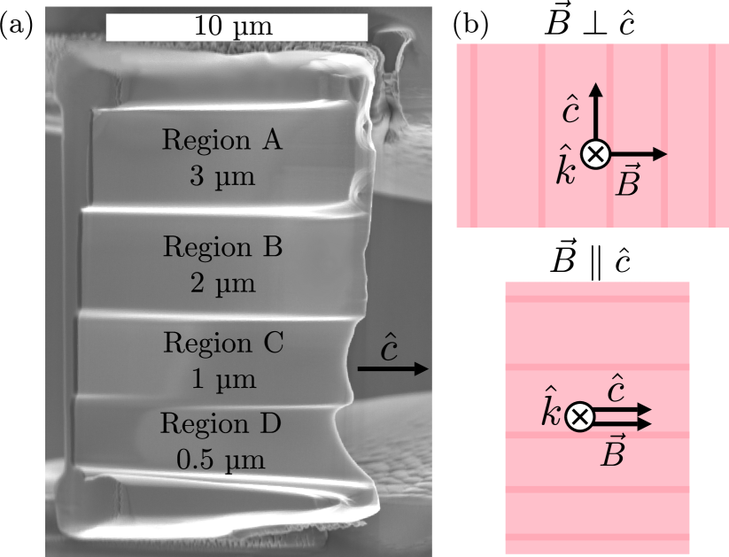
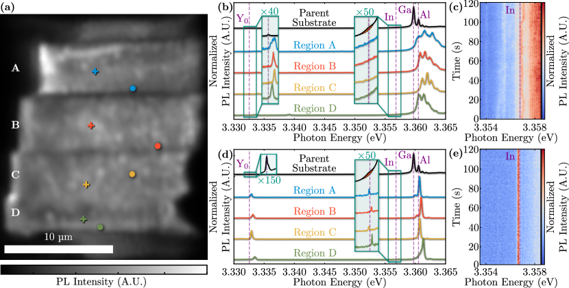
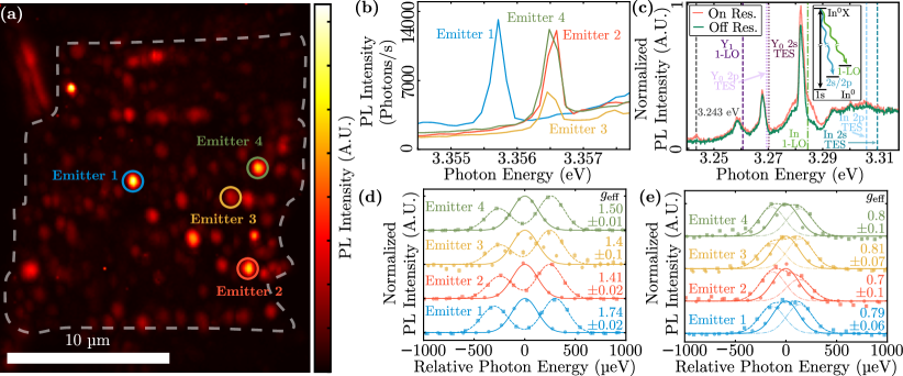
Fig. 2a displays a confocal PL image of the lamella post-annealing. PL spectra from the substrate and each region of the pre-annealed lamella are shown in Fig. 2b. The substrate spectrum shows a small shoulder at the In0X transition [12] with a peak intensity roughly times that of the Ga0X peak. Based on the measured Ga density and assuming that the relative peak intensity and donor concentration are proportional, we estimate In donors/cm3. With an excitation spot diameter of 450 nm, a 5 µm thick slice of the substrate would yield one In donor per excitation spot, with smaller concentrations for the µm thick steps of the lamella.
A weak Y0 line, related to excitons bound to structural defects [12], is observed in the substrate PL. After PFIB fabrication, an increase in the Y0 PL intensity relative to the Ga0X and Al0X lines is observed, which we ascribe to the creation of structural defects during fabrication(Fig. 2b). Additionally, an overall PL shift varying across the lamella is observed, consistent with differential strain environments. Within a single excitation spot, the Ga0X and Al0X lines also show splitting and broadening which we attribute to microscopic strain (Fig. 2b).
We monitored the PL spectra as a function of time in kinetic series measurements; Fig. 2c shows a series from region C. Multiple weak features are observed, with a stronger line at the In0X transition. Similar features are observed at multiple locations in the lamella (Supplemental Material [16], Sec. LABEL:si:donor_stability). These stronger emitters at the In0X transition exhibit discrete spectral jumps, a behavior characteristic of isolated single emitters in an unstable environment [49, 50, 51].
After annealing, the broad Ga0X and Al0X lines become single, sharp transitions, suggesting that annealing removed a majority of the milling-induced damage (Fig. 2d). A small overall PL shift persists after annealing. Interestingly, the intensity of the Ga0X line relative to the Al0X line is greatly diminished when compared to the substrate PL. The cause of this reduction is unknown.
Near the In0X line we now observe spots with strong, spectrometer-resolution limited emission (Fig. 2d right inset). A representative PL kinetic series is shown in Fig. 2(e). Compared to the pre-annealed PL spectrum, the PL emission at the In0X transition becomes stronger and spectrally stable. Additionally, the weaker features around the In0X region are no longer observed, suggesting that they may have been surface-related shallow defects which were eliminated via annealing [52].
To spatially resolve single In donors, we perform confocal PL scans while spectrally filtering the In0X emission; the resulting image is shown in Fig. 3a. Localized emission with spectrometer-resolution limited linewidths at In0X are observed (Fig. 3b). The highest density of emitters is found in regions B and C rather than the thicker region A. We note that the the total PL intensity is also brighter in these regions (Fig. 2a) and suspect that the PL intensity may be dominated by surface-related non-radiative recombination. While 5 keV PFIB polishing was performed across the entire sample, different regions were polished by different amounts which could account for the variation in PL intensity.
For the remainder of the paper, we focus on four emitters whose positions are labelled in Fig. 3a. The PL spectra corresponding to each emitter is shown in Fig. 3b, where the spectra has been shifted utilizing the location of the Al0X and Y0 lines to adjust for relative energy offsets induced by strain (Supplemental Material [16], Sec. LABEL:si:emitter_PL).
To verify these emitters as In donors, we resonantly excite the transition between the In0() state to the In0X state and collect the PL sideband consisting of the 1-LO phonon-replica and the two-electron satellites (TES) transitions. The TES transitions correspond to relaxation from the lowest In0X state to the excited and states of In0 (Fig 3c inset). Fig 3c displays the sideband PL for emitter 2 with both on- and off-resonant excitation (see Supplemental Material [16], Sec. LABEL:si:res_tes for emitters 3 and 4). For emitters 2–4, resonant PL enhancement is observed at the In 1-LO, 2s and 2p TES transitions [12], as well as an unidentified In-related transition at 3.243 eV (Supplemental Material [16], Sec. LABEL:fig:tes_em3_em4_implnt). We observe a large background in the In sideband PL. We believe that this is sideband PL from the tails of the much brighter Al0X and Ga0X zero-phonon transitions upon which the In0X transition resides. In contrast with the In-assigned sideband PL, the sideband PL background shifts with laser excitation energy. Resonant sideband enhancement is not observed for emitter 1.
We perform magneto-photoluminescence (magneto-PL) measurements with both and to verify that the observed Zeeman splittings are consistent with emission from neutral donors. Fig. 3d (Fig. 3e) shows the PL of each emitter at 0 T and 6 T with (). In both orientations, we only collect linearly polarized emission perpendicular to the crystal axis , which is expected to be 50 times larger than linearly polarized emission parallel to (Supplemental Material [16], Sec. LABEL:si:pol_rules and Refs. [23, 24, 25]). This strong polarization dependence is also experimentally observed (Supplemental Material [16], Sec. LABEL:si:pol_rules). The effective factor () for each orientation is calculated according to , where denotes the energy splitting of bound exciton transitions and denotes the Bohr magneton. This splitting results from the hole Zeeman splitting of D0X and the electron Zeeman splitting of D0. The hole factor () is then calculated according to (), where [14, 53].
In both orientations, the emission of all emitters splits into two peaks linearly dependent on field (Supplemental Material [16] Sec. LABEL:si:magnetoPL), consistent with a donor. If a donor electron is not present, as is the case for an ionized donor-bound exciton, electron-hole coupling yields a non-linear dependence [53]. Measured hole factors are consistent with ensemble measurements[53, 25, 13]. With , we find to range between and for all emitters. With , we find for emitter 1, and between and for emitters 2–4, which qualitatively follows the literature where reported values vary between and .
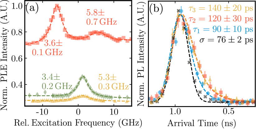
We utilize photoluminescence excitation (PLE) spectroscopy to determine the linewidth and spectral stability of emitters 2–4. In PLE measurements, we resonantly scan a continuous-wave laser over the In InX transition and collect sideband PL (Fig. 3c). The spectral stability under resonant excitation, with energy less than the ZnO band gap, supports that the donors remain in the neutral charge state in the absence of semiconductor carrier generation. This could be an advantage compared to deep-level defects such as the nitrogen-vacancy center in diamond which undergo two-photon ionization under resonant excitation [54] and require a charge repump laser [49, 50].
As shown in Fig. 4a, the high resolution PLE spectroscopy enables us to determine the absorption linewidth and also resolve multiple emitters. For example, for emitter 2 we observe a weak second peak corresponding to a second emitter. The emitter linewidths range between 3.4 GHz and 5.8 GHz.
The expected linewidth of a lifetime-limited emitter at 5.2 K is estimated by adding three different contributions. First, the line is split by 0.5 GHz due to the zero-field hyperfine interaction between the donor electron spin- and the In nuclear spin- ( MHz) [27, 26]). At 0 K, the two hyperfine lines would have a lifetime-limited linewidth of 120–150 MHz, given by the reported In ensemble lifetime [12, 21]. Each line is further broadened by 0.65 GHz due to a phonon-assisted thermal population relaxation between D0X states at 5.2 K [15]. Under these effects, the two lines are not resolvable, with a total effective linewidth of 1.2 GHz; times smaller than the observed values. Additionally, the disparity between the expected and measured linewidths could be a result of a shortened lifetime compared to the literature value.
We performed time-resolved PL measurements using pulsed laser excitation to probe the emitter lifetime. As shown in Fig. 4b, we observe excited state lifetimes between 90 ps and 140 ps, one order of magnitude smaller than expected [21]. Surface-related non-radiative recombination has been suggested to explain the energy-dependent D0X lifetime in bulk ZnO, where high-energy excitation absorbed near the ZnO surface results in shorter measured lifetimes [21]. The intensity of the emission does not increase when lowering the temperature to 2 K (Supplemental Material [16], Sec. LABEL:si:temp_dep), suggesting that the recombination mechanism is not thermally activated. The diminished lifetimes in the lamella correspond to an estimated radiative efficiency of 10 % and estimated lifetime-limited linewidths ranging from GHz, depending on the emitter. The total homogeneous linewidth increases to GHz once contributions due to phonons and the hyperfine interaction are included; hence, the measured linewidth, while only times larger than the lifetime-limited linewidth, has an additional unidentified broadening component of GHz. To realize spin-selective excitation, the non-radiative relaxation and this additional broadening mechanism need to be understood and eliminated.
In summary, we have demonstrated the isolation of single neutral shallow donors in ZnO by employing plasma focused ion beam milling techniques to isolate a small volume of ZnO. Through resonant excitation and magneto-PL, we identify three emitters as In donors. The isolated donors exhibit near lifetime-limited linewidths with charge-stable emission. The estimated 10 % radiative efficiency motivates future dedicated studies on surface damage and understanding of surface effects on near-surface quantum emitters in ZnO. However, ZnO is a fairly new quantum defect host and the relative ease of single donor isolation and observed signal recovery after one annealing step is promising. Additionally, the FIB-robust optical signal suggests FIB is appropriate for optical device fabrication in ZnO. Compatibility with FIB processing is important due to the monolithic nature of high-purity ZnO and the need for features small/comparable to the 369 nm transition wavelength. Finally, we note that this work further motivates the need for both high purity ZnO material to reduce the band-edge luminescence from unintentional dopants.
The authors thank Yusuke Kozuka for the bulk ZnO substrates. This material is based on work primarily supported by the U.S. Department of Energy (DOE), Office of Science, Office of Basic Energy Sciences, under Award No. DE-SC0020378, and partially supported by the National Science Foundation under Grant No. 1820614 and 2212017. B.E.M. and S.R.S. were supported for electron microscopy and interpretation by the DOE Office of Science National Quantum Information Science Research Centers, Co-design Center for Quantum Advantage (C2QA) under contract number DE-SC0012704. Pacific Northwest National Laboratory is a multiprogram national laboratory operated for the U.S. Department of Energy (DOE) by Battelle Memorial Institute under Contract No. DE- AC05-76RL0-1830. Lifetime measurements were supported by the National Science Foundation DMR-2212017. SIMS was supported through project No. 325573, funded by the Norwegian research council.
References
- Benjamin et al. [2009] S. Benjamin, B. Lovett, and J. Smith, Prospects for measurement-based quantum computing with solid state spins, Laser & Photonics Reviews 3, 556 (2009).
- Weber et al. [2010] J. R. Weber, W. F. Koehl, J. B. Varley, A. Janotti, B. B. Buckley, C. G. V. de Walle, and D. D. Awschalom, Quantum computing with defects, Proceedings of the National Academy of Sciences 107, 8513 (2010).
- Ladd et al. [2010] T. D. Ladd, F. Jelezko, R. Laflamme, Y. Nakamura, C. Monroe, and J. L. O’Brien, Quantum computers, Nature 464, 45 (2010).
- Wehner et al. [2018] S. Wehner, D. Elkouss, and R. Hanson, Quantum internet: A vision for the road ahead, Science 362, eaam9288 (2018).
- Orieux and Diamanti [2016] A. Orieux and E. Diamanti, Recent advances on integrated quantum communications, Journal of Optics 18, 083002 (2016).
- He et al. [2013] Y. He, Y.-M. He, Y.-J. Wei, X. Jiang, M.-C. Chen, F.-L. Xiong, Y. Zhao, C. Schneider, M. Kamp, S. Höfling, C.-Y. Lu, and J.-W. Pan, Indistinguishable tunable single photons emitted by spin-flip raman transitions in ingaas quantum dots, Phys. Rev. Lett. 111, 237403 (2013).
- De Greve et al. [2012] K. De Greve, L. Yu, P. L. McMahon, J. S. Pelc, C. M. Natarajan, N. Y. Kim, E. Abe, S. Maier, C. Schneider, M. Kamp, S. Höfling, R. H. Hadfield, A. Forchel, M. M. Fejer, and Y. Yamamoto, Quantum-dot spin–photon entanglement via frequency downconversion to telecom wavelength, Nature 491, 421 (2012).
- Gao et al. [2012] W. B. Gao, P. Fallahi, E. Togan, J. Miguel-Sanchez, and A. Imamoglu, Observation of entanglement between a quantum dot spin and a single photon, Nature 491, 426 (2012).
- Niaouris et al. [2022] V. Niaouris, M. V. Durnev, X. Linpeng, M. L. K. Viitaniemi, C. Zimmermann, A. Vishnuradhan, Y. Kozuka, M. Kawasaki, and K.-M. C. Fu, Ensemble spin relaxation of shallow donor qubits in ZnO, Phys. Rev. B 105, 195202 (2022).
- Tyryshkin et al. [2012] A. M. Tyryshkin, S. Tojo, J. J. L. Morton, H. Riemann, N. V. Abrosimov, P. Becker, H.-J. Pohl, T. Schenkel, M. L. W. Thewalt, K. M. Itoh, and S. A. Lyon, Electron spin coherence exceeding seconds in high-purity silicon, Nature Materials 11, 143 (2012).
- Balasubramanian et al. [2009] G. Balasubramanian, P. Neumann, D. Twitchen, M. Markham, R. Kolesov, N. Mizuochi, J. Isoya, J. Achard, J. Beck, J. Tissler, V. Jacques, P. R. Hemmer, F. Jelezko, and J. Wrachtrup, Ultralong spin coherence time in isotopically engineered diamond, Nature Materials 8, 383 (2009).
- Wagner et al. [2011] M. R. Wagner, G. Callsen, J. S. Reparaz, J.-H. Schulze, R. Kirste, M. Cobet, I. A. Ostapenko, S. Rodt, C. Nenstiel, M. Kaiser, A. Hoffmann, A. V. Rodina, M. R. Phillips, S. Lautenschläger, S. Eisermann, and B. K. Meyer, Bound excitons in ZnO: Structural defect complexes versus shallow impurity centers, Phys. Rev. B 84, 035313 (2011).
- Linpeng et al. [2018] X. Linpeng, M. L. Viitaniemi, A. Vishnuradhan, Y. Kozuka, C. Johnson, M. Kawasaki, and K.-M. C. Fu, Coherence properties of shallow donor qubits in , Phys. Rev. Applied 10, 064061 (2018).
- Wang et al. [2023] X. Wang, C. Zimmermann, M. Titze, V. Niaouris, E. R. Hansen, S. H. D’Ambrosia, L. Vines, E. S. Bielejec, and K.-M. C. Fu, Properties of donor qubits in formed by indium-ion implantation, Phys. Rev. Appl. 19, 054090 (2023).
- Niaouris et al. [2023] V. Niaouris, S. H. D’Ambrosia, C. Zimmermann, X. Wang, E. R. Hansen, M. Titze, E. S. Bielejec, and K.-M. C. Fu, Contributions to the optical linewidth of shallow donor - bound excitonic transition in ZnO (2023), arXiv:2307.12566 [quant-ph] .
- [16] See Supplemental Material at [URL will be inserted by publisher] for supplamentary measurements, and additional details of experimental methods, which includes Refs. [17, 18, 19, 20, 21, 22, 23, 24, 25].
- Dexter [1958] D. Dexter, Theory of the optical properties of imperfections in nonmetals, in Advances in Research and Applications, Solid State Physics, Vol. 6, edited by F. Seitz and D. Turnbull (Academic Press, 1958) pp. 353–411.
- Hilborn [1982] R. C. Hilborn, Einstein coefficients, cross sections, f values, dipole moments, and all that, American Journal of Physics 50, 982 (1982).
- Meyer et al. [2004] B. K. Meyer, H. Alves, D. M. Hofmann, W. Kriegseis, D. Forster, F. Bertram, J. Christen, A. Hoffmann, M. Straßburg, M. Dworzak, U. Haboeck, and A. V. Rodina, Bound exciton and donor–acceptor pair recombinations in ZnO, physica status solidi (b) 241, 231 (2004).
- Rössler et al. [1999] U. Rössler, R. Blachnik, J. Chu, R. Galazka, J. Geurts, J. Gutowski, B. Hönerlage, D. Hofmann, J. Kossut, R. Levy, et al., II-VI and I-VII Compounds; Semimagnetic Compounds: Supplement to Vols. III/17b, 22a (Print Version) Revised and Updated Edition of Vols. III/17b, 22a (CD-ROM), Landolt-Börnstein: Numerical Data and Functional Relationships in Science and Technology - New Series (Springer Berlin Heidelberg, 1999).
- Chen et al. [2013] S. L. Chen, W. M. Chen, and I. A. Buyanova, Dynamics of donor bound excitons in ZnO, Applied Physics Letters 102, 121103 (2013).
- Nichelatti [2002] E. Nichelatti, Complex refractive index of a slab from reflectance and transmittance: analytical solution, Journal of Optics A: Pure and Applied Optics 4, 400 (2002).
- Linpeng [2020] X. Linpeng, Donor Qubits in Direct Band GaP Materials, Ph.D. thesis, University of Washington (2020).
- Lambrecht et al. [2002] W. R. L. Lambrecht, A. V. Rodina, S. Limpijumnong, B. Segall, and B. K. Meyer, Valence-band ordering and magneto-optic exciton fine structure in ZnO, Phys. Rev. B 65, 075207 (2002).
- Wagner et al. [2009] M. R. Wagner, J.-H. Schulze, R. Kirste, M. Cobet, A. Hoffmann, C. Rauch, A. V. Rodina, B. K. Meyer, U. Röder, and K. Thonke, valence band symmetry related hole fine splitting of bound excitons in zno observed in magneto-optical studies, Phys. Rev. B 80, 205203 (2009).
- Block et al. [1982] D. Block, A. Hervé, and R. T. Cox, Optically detected magnetic resonance and optically detected ENDOR of shallow indium donors in ZnO, Phys. Rev. B 25, 6049 (1982).
- Gonzalez et al. [1982] C. Gonzalez, D. Block, R. Cox, and A. Herve´, Magnetic resonance studies of shallow donors in zinc oxide, Journal of Crystal Growth 59, 357 (1982).
- Buß et al. [2016] J. H. Buß, J. Rudolph, T. A. Wassner, M. Eickhoff, and D. Hägele, Optical manipulation of a multilevel nuclear spin in ZnO: Master equation and experiment, Phys. Rev. B 93, 155204 (2016).
- Neumann et al. [2008] P. Neumann, N. Mizuochi, F. Rempp, P. Hemmer, H. Watanabe, S. Yamasaki, V. Jacques, T. Gaebel, F. Jelezko, and J. Wrachtrup, Multipartite entanglement among single spins in diamond, Science 320, 1326 (2008).
- Morton et al. [2008] J. J. L. Morton, A. M. Tyryshkin, R. M. Brown, S. Shankar, B. W. Lovett, A. Ardavan, T. Schenkel, E. E. Haller, J. W. Ager, and S. A. Lyon, Solid-state quantum memory using the 31p nuclear spin, Nature 455, 1085 (2008).
- Merkel et al. [2008] S. T. Merkel, P. S. Jessen, and I. H. Deutsch, Quantum control of the hyperfine-coupled electron and nuclear spins in alkali-metal atoms, Physical Review A 78, 023404 (2008).
- Viitaniemi et al. [2022] M. L. K. Viitaniemi, C. Zimmermann, V. Niaouris, S. H. D’Ambrosia, X. Wang, E. S. Kumar, F. Mohammadbeigi, S. P. Watkins, and K.-M. C. Fu, Coherent spin preparation of indium donor qubits in single ZnO nanowires, Nano Letters 22, 2134 (2022), pMID: 35108020.
- Smith et al. [2019] J. M. Smith, S. A. Meynell, A. C. B. Jayich, and J. Meijer, Colour centre generation in diamond for quantum technologies, Nanophotonics 8, 1889 (2019).
- Durand et al. [2021] A. Durand, Y. Baron, W. Redjem, T. Herzig, A. Benali, S. Pezzagna, J. Meijer, A. Y. Kuznetsov, J.-M. Gérard, I. Robert-Philip, M. Abbarchi, V. Jacques, G. Cassabois, and A. Dréau, Broad diversity of near-infrared single-photon emitters in silicon, Phys. Rev. Lett. 126, 083602 (2021).
- Karasahin et al. [2022] A. Karasahin, R. M. Pettit, N. von den Driesch, M. M. Jansen, A. Pawlis, and E. Waks, Single quantum emitters with spin ground states based on cl bound excitons in znse, Phys. Rev. A 106, L030402 (2022).
- Melngailis [1987] J. Melngailis, Focused ion beam technology and applications, Journal of Vacuum Science & Technology B: Microelectronics Processing and Phenomena 5, 469 (1987).
- Matsui and Ochiai [1996] S. Matsui and Y. Ochiai, Focused ion beam applications to solid state devices, Nanotechnology 7, 247 (1996).
- Tseng [2005] A. A. Tseng, Recent developments in nanofabrication using focused ion beams, Small 1, 924 (2005).
- Moll [2018] P. J. Moll, Focused ion beam microstructuring of quantum matter, Annual Review of Condensed Matter Physics 9, 147 (2018).
- Luca et al. [2016] E. D. Luca, R. Sanatinia, S. Anand, and M. Swillo, Focused ion beam milling of gallium phosphide nanostructures for photonic applications, Opt. Mater. Express 6, 587 (2016).
- Ho et al. [2007] Y.-L. D. Ho, R. Gibson, C. Y. Hu, M. J. Cryan, J. G. Rarity, P. J. Heard, J. A. Timpson, A. M. Fox, M. S. Skolnick, M. Hopkinson, and A. Tahraoui, Focused ion beam etching for the fabrication of micropillar microcavities made of III-V semiconductor materials, Journal of Vacuum Science & Technology B: Microelectronics and Nanometer Structures Processing, Measurement, and Phenomena 25, 1197 (2007).
- Manoccio et al. [2021] M. Manoccio, M. Esposito, A. Passaseo, M. Cuscunà, and V. Tasco, Focused Ion Beam Processing for 3D Chiral Photonics Nanostructures, Micromachines 12, 10.3390/mi12010006 (2021).
- Zhong et al. [2018] T. Zhong, J. M. Kindem, J. G. Bartholomew, J. Rochman, I. Craiciu, V. Verma, S. W. Nam, F. Marsili, M. D. Shaw, A. D. Beyer, and A. Faraon, Optically addressing single rare-earth ions in a nanophotonic cavity, Phys. Rev. Lett. 121, 183603 (2018).
- Rubanov and Munroe [2004] S. Rubanov and P. Munroe, FIB-induced damage in silicon, Journal of Microscopy 214, 213 (2004).
- Rubanov and Munroe [2005] S. Rubanov and P. Munroe, Damage in III–V Compounds during Focused Ion Beam Milling, Microscopy and Microanalysis 11, 446–455 (2005).
- Bayn et al. [2011] I. Bayn, A. Bolker, C. Cytermann, B. Meyler, V. Richter, J. Salzman, and R. Kalish, Diamond processing by focused ion beam—surface damage and recovery, Applied Physics Letters 99, 10.1063/1.3658631 (2011).
- Sarcan et al. [2023] F. Sarcan, N. J. Fairbairn, P. Zotev, T. Severs-Millard, D. J. Gillard, X. Wang, B. Conran, M. Heuken, A. Erol, A. I. Tartakovskii, T. F. Krauss, G. J. Hedley, and Y. Wang, Understanding the impact of heavy ions and tailoring the optical properties of large-area monolayer ws2 using focused ion beam, npj 2D Materials and Applications 7, 23 (2023).
- Kucheyev et al. [2002] S. O. Kucheyev, P. N. K. Deenapanray, C. Jagadish, J. S. Williams, M. Yano, K. Koike, S. Sasa, M. Inoue, and K.-i. Ogata, Electrical isolation of ZnO by ion bombardment, Applied Physics Letters 81, 3350 (2002).
- Chakravarthi et al. [2021] S. Chakravarthi, C. Pederson, Z. Kazi, A. Ivanov, and K.-M. C. Fu, Impact of surface and laser-induced noise on the spectral stability of implanted nitrogen-vacancy centers in diamond, Phys. Rev. B 104, 085425 (2021).
- van Dam et al. [2019] S. B. van Dam, M. Walsh, M. J. Degen, E. Bersin, S. L. Mouradian, A. Galiullin, M. Ruf, M. IJspeert, T. H. Taminiau, R. Hanson, and D. R. Englund, Optical coherence of diamond nitrogen-vacancy centers formed by ion implantation and annealing, Phys. Rev. B 99, 161203 (2019).
- Ourari et al. [2023] S. Ourari, Ł. Dusanowski, S. P. Horvath, M. T. Uysal, C. M. Phenicie, P. Stevenson, M. Raha, S. Chen, R. J. Cava, N. P. de Leon, and J. D. Thompson, Indistinguishable telecom band photons from a single Er ion in the solid state, Nature 620, 977 (2023).
- Feng et al. [2021] C. Feng, L. Wu, P. Chen, T. Yang, B. Yu, and L. Qian, Repairing slight damages on monocrystalline silicon surface by thermal annealing, Materials Research Express 8, 045005 (2021).
- Rodina et al. [2004] A. V. Rodina, M. Strassburg, M. Dworzak, U. Haboeck, A. Hoffmann, A. Zeuner, H. R. Alves, D. M. Hofmann, and B. K. Meyer, Magneto-optical properties of bound excitons in ZnO, Phys. Rev. B 69, 125206 (2004).
- Aslam et al. [2013] N. Aslam, G. Waldherr, P. Neumann, F. Jelezko, and J. Wrachtrup, Photo-induced ionization dynamics of the nitrogen vacancy defect in diamond investigated by single-shot charge state detection, New Journal of Physics 15, 013064 (2013).