Epitaxial Y1Ba2Cu3O7 thin films on CeO2 buffer layers on sapphire substrates
Abstract
Pulsed laser deposition has been used to deposit Y1Ba2Cu307 layer on CeO2 buffer layers on (1102) sapphire. Both layers are epitaxial with the (110) direction of the CeO2 layer aligned with the 2021 direction of the sapphire substrate. The c-axis Y1Ba2Cu3O7 layer has its 100 direction aligned with the 110 direction of the CeO2. Cross-sectional transmission electron microscopy shows the epitaxy to be coherent and the interfaces to be abrupt at an atomic level. The best films have a critical current of A/cm2 at 4.2 K and lower microwave surface resistance than copper at 77 K and at a frequency of 31 GHz.
Electronic applications of high-temperature superconductor (HTS) thin films require films with high critical currents and uniform properties over the entire surface of the substrate. Due to the extreme anisotropy and short coherence lengths of HTS materials, thin films must be epitaxial in order to have the above properties. Good quality HTS films have been grown on substrates such as SrTiO3, MgO, yttria stabilized zirconia, and LaA1O3. These substrates have various shortcomings for electronic applications; high microwave losses, high dielectric constants, low mechanical strength, high cost, and lack of availability of large good quality single crystals. On the other hand, Si and sapphire (Al2O3) are excellent electronic materials and are commercially available in the form of essentially perfect, single-crystal wafers with epitaxial quality surfaces. Unfortunately, Si and Al react chemically with HTS materials at the thin-film growth temperatures. Attempts to grow HTS films directly on Si or sapphire use low growth temperatures and high deposition rates as well as requiring thick films to get away from the reacted interface.Berezin ; Boyce These techniques are in opposition to the requirements of epitaxial growth. A possible solution to this problem is to use a chemical diffusion barrier. The requirements of such a buffer layer are that it should not react significantly with the substrate or the HTS film and the layer must grow epitaxially on the substrate as well as allow the subsequent HTS layer to be epitaxial.Wu ; Wiener-Avnear ; Talvacchio ; Kingston ; Wu2
CeO2 has several properties which make it a good candidate as a buffer layer. It is a refractory material that is cubic with a lattice constant of 5.411 Å which is nearly the same lattice constant as Si. The dielectric constant of CeO2 is about 26, we do not know what its microwave frequency losses are. CeO2 has been grown epitaxially on Si by electron beam evaporation.Inoue Since Si grows epitaxially on sapphire, it is likely that CeO2 will do so also. It has also been determined that CeO2 and Y1Ba2Cu307 (YBCO) are mutually insoluble.Sampathkumaran ; Sladeczek There is a good possibility of obtaining a very clean interface on the scale of atomic ordering. We have found that CeO2 will grow epitaxially on MgO and sapphire and that good quality YBCO can be grown on the CeO2 buffer layer. In this letter, we will report on the deposition procedures and on the microstructure of YBCO on CeO2 films on (1102) oriented sapphire.
CeO2 layers were deposited by pulsed laser deposition (PLD) using techniques similar to the PLD methods that have been reported elsewhere.Boyce ; Wu3 The depositions were made in 0.20 Torr of oxygen, using a 248 nm HeF eximer laser focused to a spot giving a fluence of about 3 J cm-2. The substrate is mounted, using silver paint, on an Al2O3 ceramic plate which is heated from behind by a nickel-chromium resistive heating ribbon. Substrate temperatures, measured using an optical pyrometer, of about 740 °C are used for the CeO2 deposition.
The CeO2 layers used as buffer layers for YBCO were less than 20 nm thick and deposited by operating the laser at 10 Hz for a time of 120 s. The substrates were cooled in 500 Torr of oxygen and then the chamber let up to air to allow a YBCO target to be exchanged for the CeO2 target. A YBCO layer was then grown following the same procedure as was used for the Ce02 layer except for a slightly lower substrate temperature of 720 °C. YBCO layers between 300 and 500 nm thick were grown over deposition times of 20 to 35 min.
In this report we will concentrate on structural analysis, however we will first present a summary of electrical properties. The resistance ratio R(295 K)/R(100 K) is about 2.8 for these films. The better films have a sharp transition with zero resistance above K, whereas poorer films have a tail in the resistive transition but still go to zero resistance above K. The normal resistance of 260 µΩ cm at 295 K and 950 cm at 100 K are about the same as typical values quoted in the literature for YBCO. Over 50% of the films we grow are in the better category. X-ray diffraction and scanning electron microscopy (SEM) examination (including electron channeling) do not reveal a difference between the two. The critical current density of a 100 µm-wide line was A cm-2 at 84 K.
The microwave surface resistance of the films was measured qualitatively by placing the films on the end of a copper cavity immersed in liquid nitrogen. The was then measured at the resonant frequency of 31 GHz. Several films have given higher ’s than a copper end plate. Our system is not sensitive enough to quantify the surface resistance of the better films.
One sample was examined by a Faraday rotation magneto-optic technique.Batalla The 1-cm-square, 3200-Å-thick YBCO film was found to shield an applied field of 9 mT over its entire surface at 4.2 K. The observed trapped field implied a critical current density of Acm-2 in a field of 20 mT.
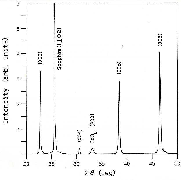
The YBCO layers are single phase c-axis oriented as shown by the x-ray diffraction spectrum in Fig. 1. The lines are strong and sharp [the half width of the (005) line is 0.26°] which is consistent with an epitaxial layer. The small peaks on the high angle side of the (003) and (006) peaks correspond with the lattice spacing of the (100) and (200) planes of the tetragonal phase, YBa2Cu3O7. The only CeO2 line present is the (200) line [we also see the (400) line at 2 = 69.5Å]. This indicates a single orientation of the Ce02 layer. The line is broadened having a width ) = 0.56°. If this broadening is due only to the thickness of the layer, the thickness can be calculated usingJames , where nm. This gives t = 16 nm which is slightly larger than the thickness measured by TEM.
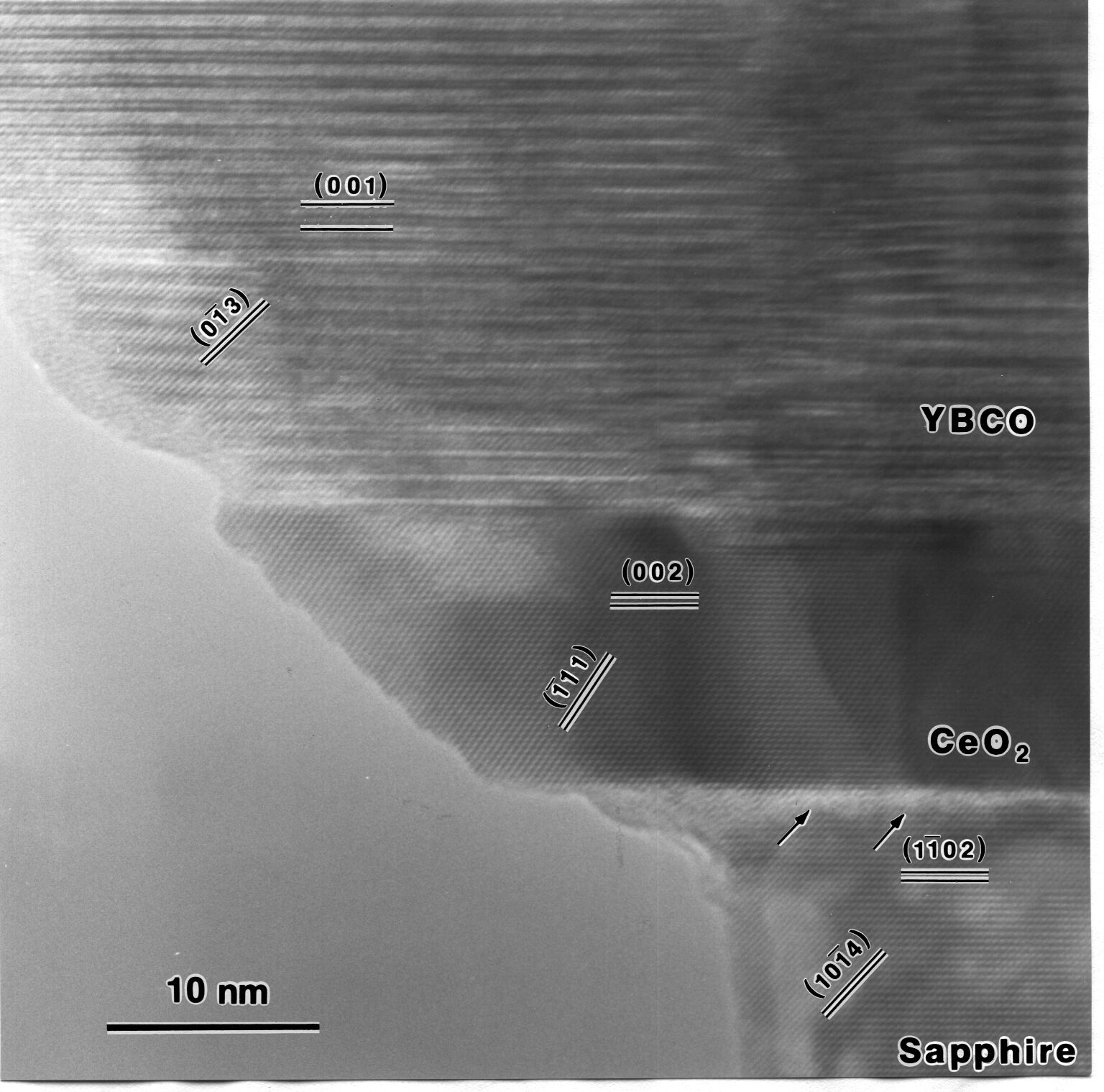
Transmission electron microscopy (TEM) was performed using a Philips EM430T operating at 250 kV. Samples were prepared by a small-angle cleavage technique described elsewhere.McCafFrey Shown in Fig. 2 is a cross section looking down the sapphire 2021 zone axis. In agreement with the XRD results the growth direction of the CeO2 is 001 and the growth direction of the YBCO is 001.
The in-plane alignment is with the (110) zone axis of the CeO2 parallel with the 2021 sapphire zone axis. The same alignment was found by electron channeling measurements made using a scanning electron microscope.
This is the same epitaxial alignment that is seen for Si on (1102) sapphire.Filby 15 The lattice mismatch is found noting that the (1120) and the (1104) planes in sapphire are parallel to the (100) and (010) planes of the CeO2. The spacings of 0.2379 and 0.2552 nm of the (1120) and the (1104) planes in sapphire have mismatches of 12% and 5.7% with the spacings CeO2 (100) planes. Any strain induced by the epitaxy due to such large lattice mismatches should be relaxed over the first two or three atomic layers by the formation of misfit dislocations. This is what we see in the cross-sectional micrograph. There is a disordered layer about two atomic rows ( nm) thick at the sapphire/Ce02 interface, which appear lighter in the micrograph due to strain contrast effects. Although the interface is disordered a majority of the (1014) sapphire planes line up with (111) Ce02 planes with an 8° tilt at the interface. This shows that the epitaxy is coherent.
The CeO2 buffer layer in Fig. 2 is about 13 nm thick. The top has atomically flat areas which appear to be separated by steps that are about 1 to 1.5 nm high. The epitaxial in-plane relation is that the (100) direction of the YBCO is parallel to the 110 CeO2 direction. Since the lattice mismatch for this orientation is less than 1%, the strain needed to accommodate the heteroepitaxy is small. This is consistent with the micrograph as there is no strain contrast at the YBCO/CeO2 interface. The (111) planes of the CeO2 are continuous with the (013) planes of the YBCO with a tilt of about 10° at the interface.
The epitaxial alignment for these layers, i.e., YBCO 100 parallel to sapphire 2021, is the same that has been observed for YBCO grown directly on (1102) sapphire.Boyce The same alignment has also been reported for YBCO on an yttria stabilized zirconia buffer layer on sapphire,Wu2 in which the buffer layer is oriented in the same way as the CeO2 reported here. It is interesting that the YBCO maintains the same alignment with the sapphire with or without a buffer layer.
We would like to comment on two further points. The good lattice match and the insolubility of Ce in YBCO make CeO2 a very good candidate for the insulating layer in a tunnel junction. This is due to the short coherence depth and the sensitivity of the superconducting properties of YBCO to strain and chemical impurities. Strain damage or chemical diffusion from the buffer layer traveling only one or two lattice constants into the YBCO would likely severely degrade tunneling properties. The results shown in Fig. 2 suggest it may be possible to grow a smooth continuous 2-nm-thick CeO2 insulating layer between two YBCO layers. The second point is that the lattice fringes of the CeO2 and sapphire extend right to the edge of the sample which had been exposed to the atmosphere for several days before TEM investigation. This is a dramatic demonstration of how these rugged materials maintain epitaxial quality surfaces. This is not true for the YBCO layer which is known from surface analysis methods to quickly develop a damaged top layer of carbonates and hydroxides.Budhani At the edge of the sample in Fig. 2, one can see an amorphous layer of about 2.5 nm thickness.
We have shown that YBCO films with excellent structural quality can be grown on sapphire with a CeO2 buffer layer. This is due to the epitaxial CeO2 buffer layer which is well lattice matched to YBCO and allows the use of a higher growth temperature than can be used for YBCO directly grown on sapphire.
The magneto-optic measurements were done by E. Batalla, some electrical measurements were done by Suso Gygax, and the microwave measurements were done by Dick Clark. We thank Peter Grant for helpful discussions. Finally, we greatly appreciate the careful work of Hue Tran who deposited the films.
References
- (1) A. B. Berezin, S. Pan, E. Ogawa, R. M. Silver, and A. L. DeLozanne, Physica C 162-164, 657 (1989).
- (2) J. B. Boyce, G. A. N. Connell, D. K. Fork, D. B. Fenner, K. Char, F. A. Ponce, F. Bridges, J. Tramontana, A. M. Viano, S. S. Laderman, R. C. Taber, S. Tahara, and T. H. Geballe, SPIE 1187, 136 ( 1989).
- (3) X. D. Wu, A. Inam, M. S. Hedge, B. Wilkens, C. C. Chang, D. M. Huang, L. Nazar, and T. Venkatesan, Appl. Phys. Lett. 54,754 (1989).
- (4) E. Wiener-Avnear, G. L. Kerber, J. E. McFall, J. W. Spar-go,and A. G. Toth, Appl. Phys. Lett. 56, 1802 (1990).
- (5) J. Talvacchio, G. R. Wagner, and H. C. Pohl, Physica C 162-164, 659 (1989).
- (6) J. J. Kingston, F. C Wellstood, P. Lench, A. H. Miklich, and J. Clarke, Appl. Phys. Lett. 56, 189 ( 1990).
- (7) X. D. Wu, R. E. Muenchausen, N. S. Nogar, A. Pique, R. Edwards, B. Wilkens, T. S. Ravi, D. M. Hwang, and C. Y. Chen, Appl. Phys. Lett. 58, 304 (1991).
- (8) T. Inoue, Y. Yamamoto, S. Koyama, S. Suzuki, and Y. Ueda, Appl. Phys. Lett. 56, 1332 (1990).
- (9) E. V. Sampathkumaran, A. Suzuki, K. Kahn, T. Shibuya, A. Tohdake, and M. Ishikawa, Jpn. J. Appl. Phys. 27, L584 (1988).
- (10) P. Sladeczek, U. Neukirch, C. T. Simmons, 0. Strebel, C. Laubschat, D. D. Sarma, and G. Kaindl, Physica C 153-155, 916 (1988).
- (11) X. D. Wu, A. Inam, T. Venkatesan, C. C. Chang, W. E. Chase, P. Barboux, J.-M Tarascon, and B. Wilkens, Appl. Phys. Lett. 52, 754 (1988).
- (12) E. Batalla, E. G. Zwartz, R. Goudrealt, and L. S. Wright, Rev. Sci. Instrum. 61, 2194 (1990).
- (13) R. W. James, Solid State Phys. 15, 169 (1963).
- (14) J. P. McCafFrey, Ultramicroscopy (to be published).
- (15) J. D. Filby and S. Nielsen, Brit. J. Appl. Phys. 18, 1357 (1967).
- (16) R. C. Budhani and M. W. Ruckman, Appl. Phys. -Lett. 55, 2354 (1989).