Continuous-wave GeSn light emitting diodes on silicon with m room-temperature emission
Abstract
Silicon-compatible short- and mid-wave infrared emitters are highly sought-after for on-chip monolithic integration of electronic and photonic circuits to serve a myriad of applications in sensing and communication. To address this longstanding challenge, GeSn semiconductors have been proposed as versatile building blocks for silicon-integrated optoelectronic devices. In this regard, this work demonstrates light-emitting diodes (LEDs) consisting of a vertical PIN double heterostructure p-Ge0.94Sn0.06/i-Ge0.91Sn0.09/n-Ge0.95Sn0.05 grown epitaxially on a silicon wafer using germanium interlayer and multiple GeSn buffer layers. The emission from these GeSn LEDs at variable diameters in the 40-120 m range is investigated under both DC and AC operation modes. The fabricated LEDs exhibit a room temperature emission in the extended short-wave range centered around 2.5 m under an injected current density as low as 45 A/cm2. By comparing the photoluminescence and electroluminescence signals, it is demonstrated that the LED emission wavelength is not affected by the device fabrication process or heating during the LED operation. Moreover, the measured optical power was found to increase monotonically as the duty cycle increases indicating that the DC operation yields the highest achievable optical power. The LED emission profile and bandwidth are also presented and discussed.
1 Introduction
Monolithic infrared (IR) solid-state light sources grown on silicon have attracted significant interest owing to their relevance to scalable photonic integrated circuits (PICs) and compatibility with complementary metal-oxide-semiconductor (CMOS) technologies 1, 2, 3. Among a plethora of applications, this monolithic integration is increasingly crucial to implementing compact and cost-effective IR sensing and imaging technologies. The former requires emitters operating at longer wavelengths in the IR range to overlap with the molecular fingerprint. For instance, emitters in the m range are useful for sensing both temperature and gas molecules such as CO, CO2, NH3, and N2O 4, 5, 6, 7, 8, 9, 10, 11, 12, 13, 14, 15. These applications call, however, for broadband emitters such as light emitting diodes (LEDs), particularly for spectroscopic detection of these critical gases generated in a chemical plant or for their atmospheric monitoring 16, 17. The current emitters serving this wavelength range consist predominantly of III-V compound semiconductors including GaSb- and InP-based device structures 18, 19, 20, 21. For instance, GaSb LEDs provide wavelength emission peaks between m and m 22, 23. Although GaSb-based lasers and super-luminescent LEDs possess higher tunability of the emitted wavelength 24, 25, 20, 26, their narrow band emission remains less favorable for spectroscopic gas detection. Notwithstanding the progress in developing III-V LEDs, these materials remain costly and their direct growth on silicon is typically associated with a degradation of device performance 27, thus hindering their integration in large-scale applications.
As an alternative, group IV GeSn semiconductors have been explored to circumvent these challenges. These semiconductors are epitaxially grown on silicon and thus can benefit from established scalable manufacturing. Moreover, the Sn content and strain can be controlled to tune the bandgap over the entire range of the IR wavelengths 28, 29, 30, 31, 32. Up-to-date, the very few reported GeSn LEDs are shown to function in the alternating current (AC) operation mode33, 34, 35, 36, 37. While AC-driven LEDs provide quasi-continuous-wave or pulse emission and mitigate the device heating by reducing the thermal power dissipation, direct current- (DC-) driven IR LEDs provide a continuous-wave emission, which is ideal for imaging and portable infrared systems that utilize DC batteries 38, 39. Herein, a GeSn vertical PIN LED with an emission peak in the range of m is demonstrated. The achieved GeSn LEDs are shown to operate under DC bias at a relatively low injection current. Before delving into the device performance, the material growth and characterization are first presented to elucidate the basic properties of the PIN heterostructure including lattice strain and Sn content. Additionally, an eight-band model is implemented to estimate the band alignment of the grown GeSn stack to evaluate the electronic structure of the obtained double heterostructure. Afterward, the electrical and optical measurements are presented to investigate the LED operation under DC- and AC-driven operation modes, the emission wavelength, the emission power profile, and the bandwidth.
2 Results and discussion
Starting from a 4-inch Si(100) wafer, a PIN GeSn double heterostructure was grown on a Ge virtual substrate (Ge-VS) using four GeSn buffer layers in a low-pressure chemical vapor deposition (CVD) reactor. The PIN GeSn layers were grown at temperatures of , , and ∘C, respectively. The growth temperature was optimized to reach the targeted content and strain while considering the possible fluctuations in Sn incorporation that occur due to the partial relaxation of strain and/or the presence of dopants 40, 41. The p- and n-type doping were achieved using diborane (B2H6) and arsine (AsH3) precursors. The obtained active doping surpasses cm-3 for both doping types, as confirmed by capacitance-voltage (C-V) measurements. A cross-sectional transmission electron micrograph (TEM) of the as-grown heterostructure is depicted in Fig.1(a) indicating a total thickness of 1.9 m from the Si/Ge-VS interface up to the sample surface. To estimate the strain and Sn composition in this stack, X-ray diffraction (XRD) reciprocal space mapping (RSM) around the asymmetrical (-2-24) reflection was acquired, as displayed in Fig.1(b). The Ge-VS peak indicates an in-plane tensile strain of % due to cyclic thermal annealing applied to improve the Ge-VS crystalline quality. However, GeSn buffer layers #1 to #4 are under a compressive strain, which remains relatively low reaching % in #3 and #4 layers. The p-Ge0.94Sn0.06 layer is fully relaxed, whereas the i-Ge0.91Sn0.09 layer shows a compressive strain of . Additionally, the pseudomorphic growth on the i-Ge0.91Sn0.09 yields a tensile strain of in the n-Ge0.95Sn0.05. As it can be seen in Fig.1(a), the thicknesses of the n-Ge0.95Sn0.05, i-Ge0.91Sn0.09, and p-Ge0.94Sn0.06 layers are , , and nm, respectively. While i- and n-layers exhibit high crystalline quality, at the TEM scale, the p-layer and the multi-layer stack underneath show dislocations and defects, especially, at the Si/Ge-VS interface, where the gliding of misfit dislocations is promoted rather than the propagation of threading dislocations toward the upper portion of the stacking.
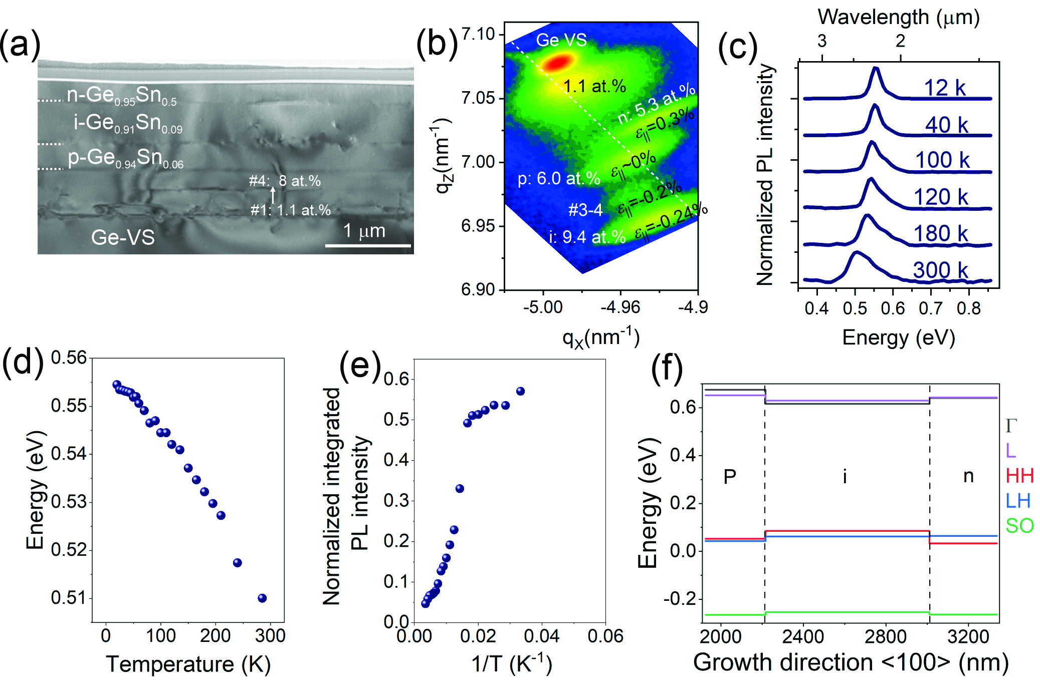
To investigate the IR emission of the as-grown PIN multi-layer structure, temperature-dependent photoluminescence (PL) measurements were carried out, as shown in Fig. 1(c). The PL spectra were measured at temperatures in the 12–300 K range. The emission peak is observed at 0.554 eV with a full width at half maximum (FWHM) of 31.8 meV at 12 K. Since the PL emission at 12 K is obtained at a low excitation power density of 231 W/cm2, the constant peak energy from 12 K till 55 K (Fig. 1(d)) is most likely attributed to shallow optically active localized levels near the bandgap edges 42. However, as the temperature increases above 55 K a progressive redshift is observed up to 300 K, as shown in Fig. 1(d). In Fig.1(e), the integrated PL intensity, normalized to that measured at 12 K, is plotted as a function of the inverse of temperature. It is noticeable that the PL emission decreases as the temperature increases, and this drop in PL is more remarkable above 55 K. It can be inferred from the monotonic increase of both PL integrated intensity (Fig.1(e)) and emission energy (Fig.1(d)) that, as the temperature decreases, the recombination is dominated by radiative mechanisms rather than phonon and impurity-ionization related nonradiative mechanisms, which is consistent with the band gap directness of the investigated heterostructure over the temperature range 12 K to 300 K 42.
Since both strain and composition can have a significant influence on the GeSn bandgap energy, an eight-band model with envelope function approximation 43 was implemented to calculate the band structure of the whole stack. The bandgap lineup in Fig.1(f) is calculated at 300 K. The eight-band k.p Ge1-xSnx material parametrization is based on that reported in early studies 44, 45, 46, while strain implementation is based on the Bir-Pikus formalism 47. To account for the inaccuracy of Vegard’s law in estimating the bandgaps of Ge1-xSnx alloys, bandgap bowing parameters are introduced for L and high-symmetry points 48, 44. The computed band alignment is displayed in Fig.1(f). It is noteworthy that the i-Ge0.91Sn0.09 layer has a smaller direct band gap of eV compared to the p-Ge0.94Sn0.06 and n-Ge0.95Sn0.05 layers which have bandgap energies of eV and eV, respectively. This result confirms the formation of a double heterostructure at the i-layer of the GeSn PIN stack. It is also noted that tensile strain in the n-layer has reduced its bandgap energy compared to that of the p-layer which contains more Sn content but a higher compressive strain.
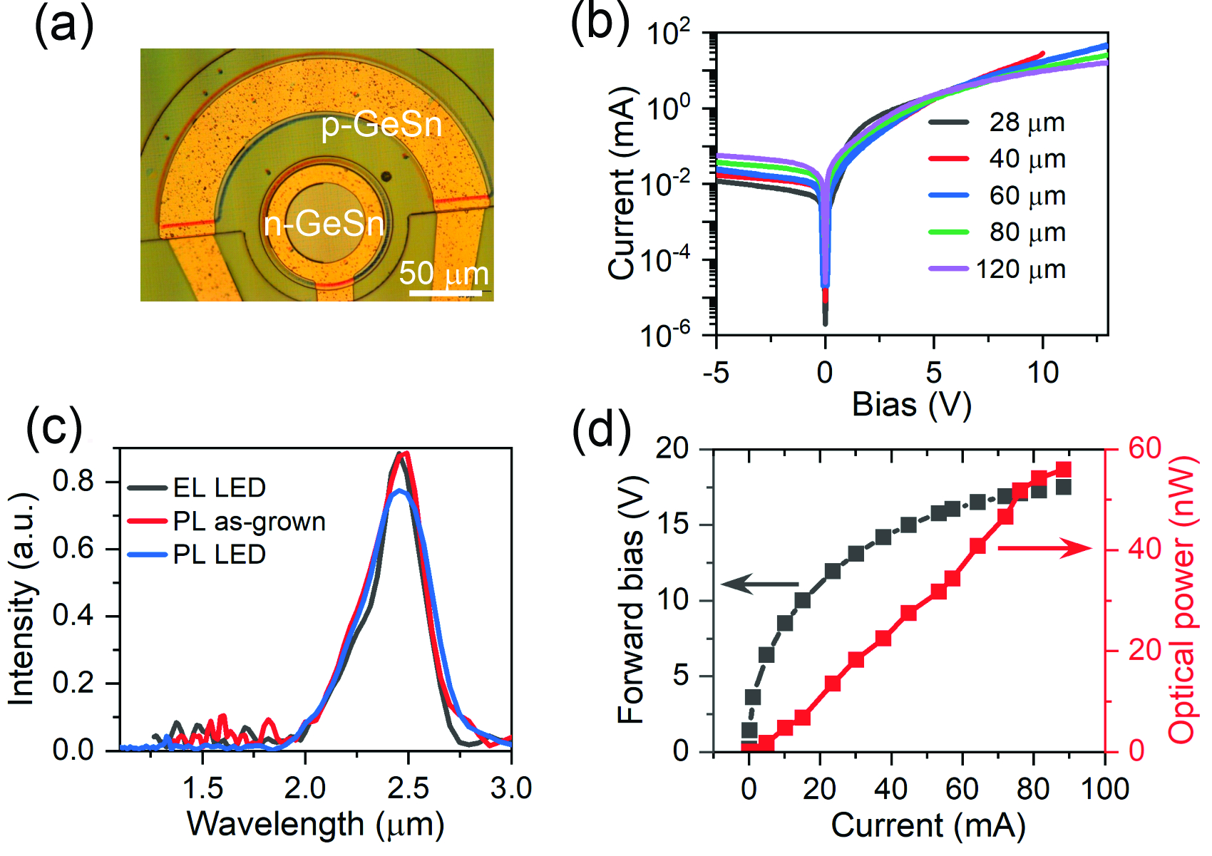
The main steps of the GeSn LED device fabrication include chlorine-based ICP dry etch down to the Ge-VS layer, etch down to the p-GeSn layer forming active circular bumps of various diameters, wet chemical passivation of the etched sidewalls followed by SiO2 deposition, BOE etch of contacts openings in the SiO2 thin-film, and, finally, e-beam deposition of Ti/Au contacts, as shown in Fig.2(a). To analyze the LED device performance under DC operation mode, the I-V curves were first measured under DC bias, as shown in Fig.2(b), for device diameters in the range of m to m. In reverse bias, the measured current ranges from 0.01 mA to 0.08 mA at -5 V as the device’s active area increases from m to m. In forward bias, the LED current reaches about 2 mA at 5 V regardless of the device diameter. This indicates that by simply down-scaling the device size, the rectification ratio increases from approximately one order of magnitude at a device diameter of m to two orders of magnitude at a diameter of m. As the DC forward bias increases to 10 V, the m device reaches breakdown at a current of about 20 mA, while it exceeds 100 mA at a bias 15 V in larger area devices.
The electroluminescence (EL) emission of the m LED at an injection current of 15 mA was spectrally analyzed using an FTIR spectrometer and liquid nitrogen (LN) cooled InSb photodetector, as displayed in Fig. 2(c). The recorded room temperature EL spectrum peaks at m. To rule out any shift in the EL peak that might result from any possible stress build-up during device fabrication or heating through the injected current, the EL spectrum was compared to the PL of both an as-grown sample and a fabricated device (Fig.2(c)). It is evident that the EL and PL peaks overlap with each other meaning that the EL peak is intrinsic to the material properties and not affected by the device fabrication process or heating during the LED operation.
The optical power emitted from the m LED was evaluated up to 90 mA yielding 58 nW, as measured by an extended InGaAs (Ex-InGaAs) commercial detector (Fig.2(d)). The emitted optical power is negligible until the DC bias exceeds 3.5 V, which constitutes the turn-on voltage of the LED. While the emitted optical power is nonlinear with the applied DC bias, it is linear with the injection current, which is most likely due to the higher bias required to increase the current injection into the double heterostructure LED. This m LED reaches breakdown at 17.8 V.
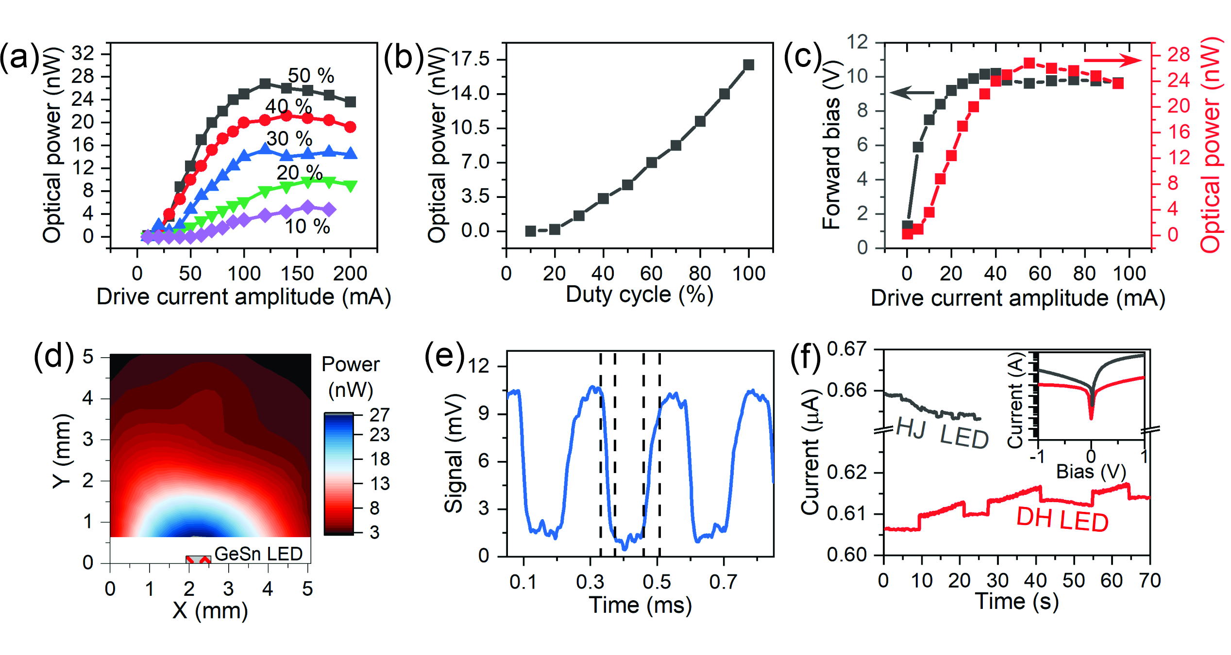
The emitted optical power under quasi-continuous wave (qCW) operation mode is investigated, as shown in Fig.3(a). The qCW is a rectangular voltage waveform applied to the LED with a preset duty cycle and injection current amplitude. As the duty cycle increases from 10% to 50%, the emitted optical power increases significantly, however, all curves reach saturation as the amplitude of the injection current exceeds 100 mA most likely because of trap-assisted leakage and non-radiative recombination. Fig.3(b) shows the emitted optical power as the duty cycle is varied from 10% to 100% at an injection current amplitude of 30 mA. The optical power is monotonically increasing as the duty cycle increases indicating that the DC operation of these LEDs would yield the highest achievable optical power.
The optical power emitted by the m LED under qCW bias of 50 % duty cycle was measured up to an amplitude of 90 mA yielding 28 nW, as shown in Fig.3(c). The emitted optical power is nonlinear with the applied bias and the injection current. This m LED reaches saturation around 10.2 V. This saturation is related to the increased injection current above 50 mA equivalent DC current and not related to the applied bias, which remains below the breakdown voltage.
In Fig.3(d), the optical power profile of the m LED is investigated. To acquire this map, the LED was mounted on a scanning stage, and an Ex-InGaAs photodetector was used to measure the emitted optical power as the x position of the LED is varied while the photodetector is moved vertically upward in the y direction after each completed x scan. It is evident that the EL emission follows a Lambertian profile and the emitted power reduces to half as the detector moves 1 mm upward. The highest power of 27 nW was recorded when the detector was closest to the LED (0.7 mm away) and the drive injection current was 45 mA through the m LED under DC operation.
The LED bandwidth is also investigated using the Ex-InGaAs photodetector and a high-bandwidth oscilloscope. The measured signal is displayed in Fig.3(e), and it indicates a fall time of s which corresponds to an LED bandwidth of Fall time, i.e. kHz. The low LED bandwidth is most likely related to an increase in the carrier lifetime plausibly caused by the trapped photocarriers at the bandgap energy step at the i-layer and p-layer interface. This was confirmed by comparing the emission of this LED to that of another PIN GeSn LED at a similar Sn content but without a noticeable energy offset at the p- and i-layer interface. The latter exhibits a higher forward bias current compared to the former but emits significantly lower power, as shown in Fig.3(f). Additionally, owing to the relatively small bandgap of the GeSn active layer, thermal radiative emission is expected to be significant,49 especially at high driving current, which also reduces the LED bandwidth.
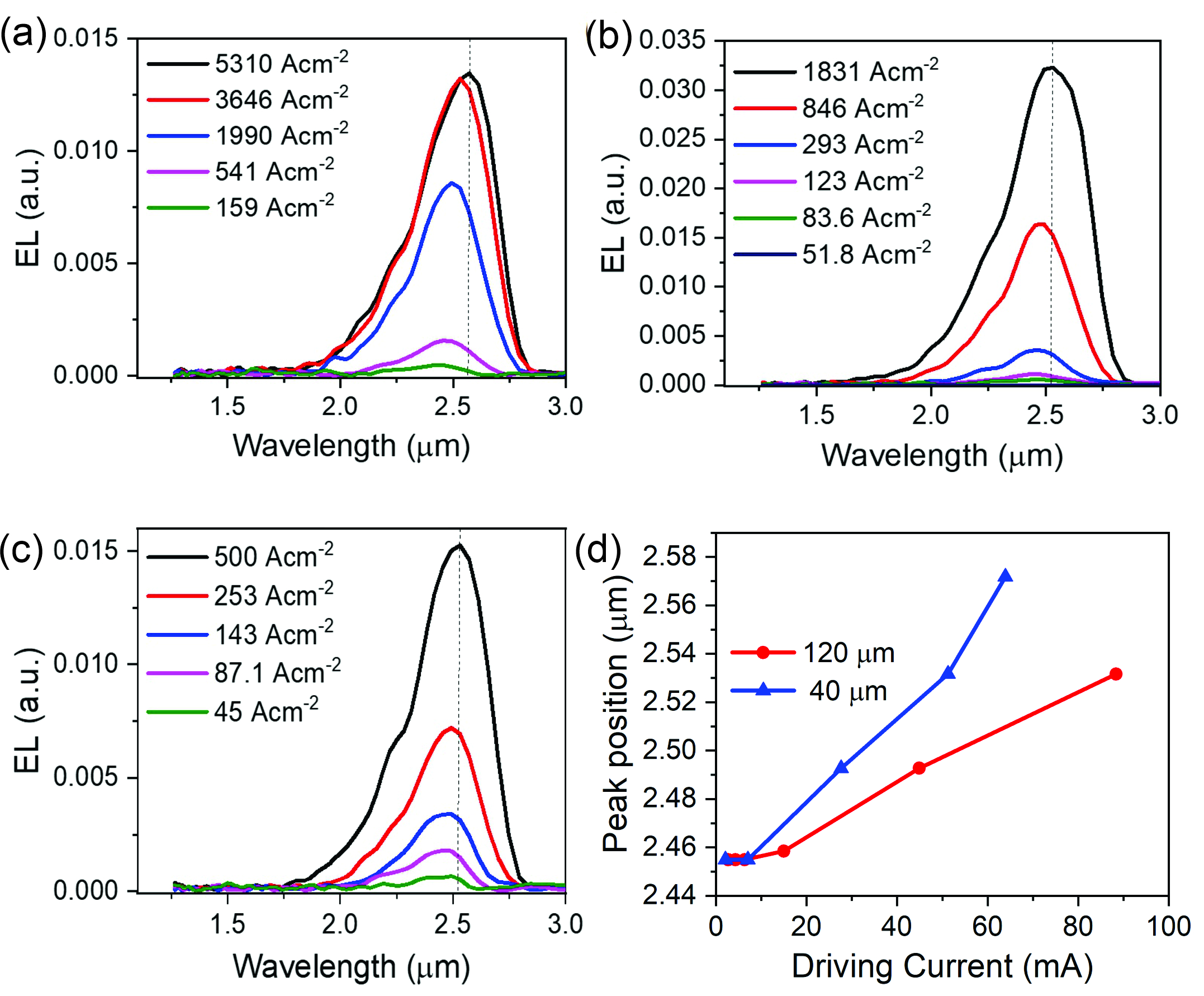
The effect of device diameter size on the emitted power and the change of emission peak position as a function of the driving current is displayed in Fig.4. The EL emission spectra from and m LEDs are measured at various DC injection levels. It is evident that as the device diameter increases, the injection current reduces. Moreover, the lowest injection current, corresponding to the smallest measurable EL, reduces from A/cm2 (m device) to A/cm2 (m device). Another observation from Fig.4 is that the EL peak redshifts as the injection current increases regardless of the device diameter. This redshift is larger in the m device as compared to the m device. More precisely, for the m device, the EL peak reaches m at the highest injection current of 500 A/cm2, whereas the injection current of 5310 A/cm2 in the m device corresponds to the EL peak position of m. The EL peaks are centered at m and m at DC injection currents of mA and mA in the m and m LEDs, respectively. The redshift of the EL peak at high current injection levels is most likely caused by the heating effect which becomes more prevalent in smaller devices.
3 Conclusion
In this work, GeSn-based extended-SWIR vertical LEDs monolithically integrated on silicon have been demonstrated. The PIN heterostructure consisting of p-Ge0.94Sn0.06/i-Ge0.91Sn0.09/n-Ge0.95Sn0.05 layers was grown following a step-graded growth protocol to control their strain and content. The obtained LEDs show an emission peak at a wavelength range of m depending on the injection current level and the LED device diameter. These LEDs have shown injection current density as low as Acm for a m diameter device and demonstrated both DC and qCW (AC) operation. The emitted power profile was found to be lambartian in shape and the highest emitted power was found to be nW at m at an injection current of mA. These LEDs show a bandwidth that is most likely attributed to an increase in the carrier lifetime due to trapped photocarriers at the i-layer and p-layer interface. The demonstrated group IV GeSn-based LEDs are promising for on-chip integrated extended-IR light emitters for compact and cost-effective gas sensing and imaging applications. However, more work is needed to improve their structural properties and optimize their performance to reach emission powers sufficiently high to be relevant for practical applications.
3.1 Funding:
The work carried out in Montréal was supported by Natural Science and Engineering Research Council of Canada (Discovery, SPG, and CRD Grants), Canada Research Chairs, Canada Foundation for Innovation, Mitacs, PRIMA Québec, Defence Canada (Innovation for Defence Excellence and Security, IDEaS), the European Union’s Horizon Europe research and innovation programme under grant agreement No 101070700 (MIRAQLS), and the US Army Research Office Grant No. W911NF-22-1-0277.
3.2 Acknowledgement:
The authors would like to thank Joel Bouchard for technical support.
References
- Powell et al. 2022 Powell, K.; Li, L.; Shams-Ansari, A.; Wang, J.; Meng, D.; Sinclair, N.; Deng, J.; Lončar, M.; Yi, X. Integrated silicon carbide electro-optic modulator. Nature Communications 2022, 13, 1851
- Kim et al. 2023 Kim, Y.; Assali, S.; Joo, H.-J.; Koelling, S.; Chen, M.; Luo, L.; Shi, X.; Burt, D.; Ikonic, Z.; Nam, D., et al. Short-wave infrared cavity resonances in a single GeSn nanowire. Nature Communications 2023, 14, 4393
- Hu et al. 2017 Hu, T.; Dong, B.; Luo, X.; Liow, T.-Y.; Song, J.; Lee, C.; Lo, G.-Q. Silicon photonic platforms for mid-infrared applications. Photonics Research 2017, 5, 417–430
- Zia et al. 2019 Zia, N.; Viheriälä, J.; Koivusalo, E.; Guina, M. High-power single mode GaSb-based 2 m superluminescent diode with double-pass gain. Applied Physics Letters 2019, 115
- Mathews et al. 2021 Mathews, G. C.; Blaisdell, M.; Lemcherfi, A. I.; Slabaugh, C. D.; Goldenstein, C. S. High-bandwidth laser-absorption measurements of temperature, pressure, CO, and H2O in the annulus of a rotating detonation rocket engine. AIAA Scitech 2021 Forum. 2021; p 0418
- Stritzke et al. 2015 Stritzke, F.; Diemel, O.; Wagner, S. TDLAS-based NH3 mole fraction measurement for exhaust diagnostics during selective catalytic reduction using a fiber-coupled 2.2-m DFB diode laser. Applied Physics B 2015, 119, 143–152
- Ji et al. 2022 Ji, Y.; Duan, K.; Lu, Z.; Ren, W. Mid-infrared absorption spectroscopic sensor for simultaneous and in-situ measurements of ammonia, water and temperature. Sensors and Actuators B: Chemical 2022, 371, 132574
- Lamoureux and Desgroux 2021 Lamoureux, N.; Desgroux, P. In situ laser-induced fluorescence and ex situ cavity ring-down spectroscopy applied to NO measurement in flames: microprobe perturbation and absolute quantification. Energy & Fuels 2021, 35, 7107–7120
- Bader et al. 2020 Bader, A.; Pfenning, A.; Schade, A.; Knebl, G.; Weih, R.; Rawal, Y.; Worschech, L.; Hartmann, F.; Höfling, S. Progress on mid-infrared optoelectronic devices: interband cascade lasers, interband cascade detectors, and resonant tunneling diodes. Infrared Remote Sensing and Instrumentation XXVIII. 2020; pp 114–123
- Ryczko et al. 2021 Ryczko, K.; Zielińska, A.; Sęk, G. Interband cascade active region with ultra-broad gain in the mid-infrared range. Materials 2021, 14, 1112
- Olafsen and Rumman 2020 Olafsen, L. J.; Rumman, N. Optically-pumped mid-infrared interband cascade lasers. 2020 IEEE Texas Symposium on Wireless and Microwave Circuits and Systems (WMCS). 2020; pp 1–4
- Dolores-Calzadilla et al. 2017 Dolores-Calzadilla, V.; Romeira, B.; Pagliano, F.; Birindelli, S.; Higuera-Rodriguez, A.; Van Veldhoven, P.; Smit, M.; Fiore, A.; Heiss, D. Waveguide-coupled nanopillar metal-cavity light-emitting diodes on silicon. Nature Communications 2017, 8, 14323
- Aziz et al. 2017 Aziz, M.; Xie, C.; Pusino, V.; Khalid, A.; Steer, M.; Thayne, I. G.; Cumming, D. R. Multispectral mid-infrared light emitting diodes on a GaAs substrate. Applied Physics Letters 2017, 111
- Shterengas et al. 2016 Shterengas, L.; Kipshidze, G.; Hosoda, T.; Wang, M.; Feng, T.; Belenky, G. Cascade type-I quantum well GaSb-based diode lasers. Photonics. 2016; p 27
- Li et al. 2018 Li, Z.-L.; Chang, B.-H.; Lin, C.-H.; Lee, C.-P. Dual-wavelength GaSb-based mid infrared photonic crystal surface emitting lasers. Journal of Applied Physics 2018, 123
- Mikhailova et al. 2007 Mikhailova, M.; Stoyanov, N.; Andreev, I.; Zhurtanov, B.; Kizhaev, S.; Kunitsyna, E.; Salikhov, K.; Yakovlev, Y. Optoelectronic sensors on GaSb-and InAs-based heterostructures for ecological monitoring and medical diagnostics. Optical Sensing Technology and Applications. 2007; pp 581–589
- Stoyanov et al. 2012 Stoyanov, N. D.; Salikhov, K. M.; Kalinina, K. V.; Zhurtanov, B. E.; Kizhaev, S. S. Middle infrared LEDs: key element for new generation chemical sensors. Optical Components and Materials IX. 2012; pp 331–336
- Dai Nguyen et al. 2022 Dai Nguyen, T.; Kim, J.; Lee, S. Growth of ingaassb/gasb compound for infrared optoelectronic devices. Condensed Matter and Interphases 2022, 24, 250–255
- Alexandrov et al. 2002 Alexandrov, S.; Gavrilov, G. A.; Kapralov, A.; Karandashev, S. A.; Matveev, B. A.; Sotnikova, G. Y.; Stus, N. M. Portable optoelectronic gas sensors operating in the mid-IR spectral range (3–5 um). Second International Conference on Lasers for Measurement and Information Transfer. 2002; pp 188–194
- Sprengel et al. 2015 Sprengel, S.; Andrejew, A.; Federer, F.; Veerabathran, G.; Boehm, G.; Amann, M.-C. Continuous wave vertical cavity surface emitting lasers at 2.5 m with InP-based type-II quantum wells. Applied Physics Letters 2015, 106
- Meyer et al. 2020 Meyer, J. R.; Bewley, W. W.; Canedy, C. L.; Kim, C. S.; Kim, M.; Merritt, C. D.; Vurgaftman, I. The interband cascade laser. Photonics. 2020; p 75
- Danilova et al. 2005 Danilova, T.; Zhurtanov, B.; Imenkov, A.; Yakovlev, Y. P. Light-emitting diodes based on GaSb alloys for the 1.6–4.4 m mid-infrared spectral range. Semiconductors 2005, 39, 1235–1266
- Tournié and Cerutti 2019 Tournié, E.; Cerutti, L. Mid-infrared optoelectronics: materials, devices, and applications; Woodhead publishing, 2019
- Coldren 2000 Coldren, L. A. Monolithic tunable diode lasers. IEEE Journal of Selected Topics in Quantum Electronics 2000, 6, 988–999
- Lee et al. 2007 Lee, B. G.; Belkin, M. A.; Audet, R.; MacArthur, J.; Diehl, L.; Pflügl, C.; Capasso, F.; Oakley, D. C.; Chapman, D.; Napoleone, A., et al. Widely tunable single-mode quantum cascade laser source for mid-infrared spectroscopy. Applied Physics Letters 2007, 91, 231101
- Karioja et al. 2017 Karioja, P.; Alajoki, T.; Cherchi, M.; Ollila, J.; Harjanne, M.; Heinilehto, N.; Suomalainen, S.; Viheriälä, J.; Zia, N.; Guina, M., et al. Multi-wavelength mid-IR light source for gas sensing. Photonic Instrumentation Engineering IV. 2017; pp 194–202
- Moutanabbir and Gösele 2010 Moutanabbir, O.; Gösele, U. Heterogeneous Integration of Compound Semiconductors. Annual Review of Materials Research 2010, 40, 469–500
- Atalla et al. 2023 Atalla, M. R.; Kim, Y.; Assali, S.; Burt, D.; Nam, D.; Moutanabbir, O. Extended-SWIR GeSn LEDs with Reduced Footprint and Efficient Operation Power. ACS Photonics 2023,
- Moutanabbir et al. 2021 Moutanabbir, O.; Assali, S.; Gong, X.; O’Reilly, E.; Broderick, C. A.; Marzban, B.; Witzens, J.; Du, W.; Yu, S.-Q.; Chelnokov, A.; Buca, D.; Nam, D. Monolithic infrared silicon photonics: The rise of (Si)GeSn semiconductors. Applied Physics Letters 2021, 118, 110502
- von den Driesch et al. 2015 von den Driesch, N.; Stange, D.; Wirths, S.; Mussler, G.; Holländer, B.; Ikonic, Z.; Hartmann, J. M.; Stoica, T.; Mantl, S.; Grützmacher, D.; Buca, D. Direct Bandgap Group IV Epitaxy on Si for Laser Applications. Chemistry of Materials 2015, 27, 4693–4702
- Buca et al. 2022 Buca, D.; Bjelajac, A.; Spirito, D.; Concepción, O.; Gromovyi, M.; Sakat, E.; Lafosse, X.; Ferlazzo, L.; von den Driesch, N.; Ikonic, Z.; Grützmacher, D.; Capellini, G.; El Kurdi, M. Room Temperature Lasing in GeSn Microdisks Enabled by Strain Engineering. Advanced Optical Materials 2022, 10, 2201024
- Wu et al. 2023 Wu, S.; Zhang, L.; Wan, R.; Zhou, H.; Lee, K. H.; Chen, Q.; Huang, Y.-C.; Gong, X.; Tan, C. S. Ge0.92 Sn0.08/Ge multi-quantum-well LEDs operated at 2 m wavelength on a 12-inch Si substrate. Photonics Research 2023, 11, 1606–1612
- Huang et al. 2019 Huang, B. J.; Chang, C. Y.; Hsieh, Y. D.; Soref, R. A.; Sun, G.; Cheng, H. H.; Chang, G. E. Electrically Injected GeSn Vertical-Cavity Surface Emitters on Silicon-on-Insulator Platforms. ACS Photonics 2019, 6, 1931–1938
- Peng et al. 2020 Peng, L.; Li, X.; Liu, Z.; Liu, X.; Zheng, J.; Xue, C.; Zuo, Y.; Cheng, B. Horizontal GeSn/Ge multi-quantum-well ridge waveguide LEDs on silicon substrates. Photonics Research 2020, 8, 899
- Stange et al. 2017 Stange, D.; von den Driesch, N.; Rainko, D.; Roesgaard, S.; Povstugar, I.; Hartmann, J.-M.; Stoica, T.; Ikonic, Z.; Mantl, S.; Grützmacher, D.; Buca, D. Short-wave infrared LEDs from GeSn/SiGeSn multiple quantum wells. Optica 2017, 4, 185
- Bertrand et al. 2019 Bertrand, M.; Pauc, N.; Thai, Q.; Chrétien, J.; Casiez, L.; Quintero, A.; Rodriguez, P.; Khazaka, R.; Aubin, J.; Hartmann, J., et al. Mid-infrared GeSn-based LEDs with Sn content up to 16%. 2019 IEEE 16th International Conference on Group IV Photonics (GFP). 2019; pp 1–2
- Gallagher et al. 2015 Gallagher, J. D.; Senaratne, C. L.; Sims, P.; Aoki, T.; Menéndez, J.; Kouvetakis, J. Electroluminescence from GeSn heterostructure pin diodes at the indirect to direct transition. Applied Physics Letters 2015, 106, 091103
- Thirumalai 2018 Thirumalai, J. Light-emitting diode: An outlook on the empirical features and its recent technological advancements; BoD–Books on Demand, 2018
- Lasance et al. 2014 Lasance, C. J.; Poppe, A., et al. Thermal management for LED applications; Springer, 2014; Vol. 2
- Assali et al. 2019 Assali, S.; Nicolas, J.; Moutanabbir, O. Enhanced Sn incorporation in GeSn epitaxial semiconductors via strain relaxation. Journal of Applied Physics 2019, 125, 025304
- Atalla et al. 2022 Atalla, M. R. M.; Assali, S.; Koelling, S.; Attiaoui, A.; Moutanabbir, O. High-Bandwidth Extended-SWIR GeSn Photodetectors on Silicon Achieving Ultrafast Broadband Spectroscopic Response. ACS Photonics 2022, 9, 1425–1433
- Assali et al. 2021 Assali, S.; Dijkstra, A.; Attiaoui, A.; Bouthillier, É.; Haverkort, J. E.; Moutanabbir, O. Midinfrared Emission and Absorption in Strained and Relaxed Direct-Band-Gap Ge 1- x Sn x Semiconductors. Physical Review Applied 2021, 15, 024031
- Bahder 1992 Bahder, T. B. Erratum: Eight-band kp model of strained zinc-blende crystals [Phys. Rev. B 41, 11 992 (1990)]. Phys. Rev. B 1992, 46, 9913–9913
- Chang et al. 2010 Chang, G.-E.; Chang, S.-W.; Chuang, S. L. Strain-Balanced GezSn1-zSixGeySn1-x-y Multiple-Quantum-Well Lasers. IEEE Journal of Quantum Electronics 2010, 46, 1813–1820
- Lu Low et al. 2012 Lu Low, K.; Yang, Y.; Han, G.; Fan, W.; Yeo, Y.-C. Electronic Band Structure and Effective Mass Parameters of Ge1-xSnx Alloys. Journal of Applied Physics 2012, 112, 103715
- Polak et al. 2017 Polak, M. P.; Scharoch, P.; Kudrawiec, R. The Electronic Band Structure of Ge1-xSnx in the Full Composition Range: Indirect, Direct, and Inverted Gaps Regimes, Band Offsets, and the Burstein–Moss Effect. Journal of Physics D: Applied Physics 2017, 50, 195103
- Bir and Pikus 1974 Bir, G. L.; Pikus, G. E. Symmetry and strain-induced effects in semiconductors; Wiley, 1974
- Bertrand et al. 2019 Bertrand, M.; Thai, Q.-M.; Chrétien, J.; Pauc, N.; Aubin, J.; Milord, L.; Gassenq, A.; Hartmann, J.-M.; Chelnokov, A.; Calvo, V.; Reboud, V. Experimental Calibration of Sn-Related Varshni Parameters for High Sn Content GeSn Layers. Annalen der Physik 2019, 531, 1800396
- Buca et al. 2022 Buca, D.; Bjelajac, A.; Spirito, D.; Concepción, O.; Gromovyi, M.; Sakat, E.; Lafosse, X.; Ferlazzo, L.; von den Driesch, N.; Ikonic, Z., et al. Room Temperature Lasing in GeSn Microdisks Enabled by Strain Engineering. Advanced Optical Materials 2022, 10, 2201024