Support-based transfer and contacting of individual nanomaterials for in-situ nanoscale investigations
Abstract
Although in-situ transmission electron microscopy (TEM) has been gaining importance in recent years, difficulties in sample preparation have limited the number of studies on electrical properties. Here, a support-based preparation method of individual 1D and 2D materials is presented, which yields a reproducible sample transfer for electrical investigation by in-situ TEM. Using a mechanically rigid support grid allows the reproducible transfer and contacting to in-situ chips by focused ion beam with minimum damage and contamination. The transfer quality is assessed by exemplary studies of different nanomaterials, including a monolayer of WS2. Preliminary results from in-situ test experiments give an overview of possible studies, which concern the interplay between structural properties and electrical characteristics on the individual nanomaterial level as well as failure analysis under electrical current or studies of electromigration, Joule heating and related effects. The TEM measurements can be enriched by additional correlative microscopy techniques, which allow the study with a spatial resolution in the range of a few microns. Although developed for in-situ TEM, the present transfer method is also applicable to transferring nanomaterials to similar chips for performing further studies or even for using them in potential electrical/optoelectronic/sensing devices.
keywords:
in-situ transmission electron microscopy , nanomaterial , sample preparation , electrical properties , focused ion beamThis is the Preprint version of our article:
1 Introduction
The detailed study of structure, composition and properties of nanomaterials is crucial to understand them in detail, to achieve an improvement of their synthesis and to yield a successful application. With respect to electrical properties of 1D nanomaterials, great effort has been invested in the characterization of numerous individual nanotubes (NTs) with the help of scanning electron microscopy (SEM) and electron-beam lithography (EBL), e.g., of carbon NTs [1, 2] but also of related structures [3, 4, 5, 6]. This approach allows the analysis of electrical properties of individual nanomaterials, but the exact structure and composition of that particular nanomaterial, including defects or dopants down to the atomic level, is typically not acquired. Thus, such studies only give ensemble values for the, e.g., conductivity and lack the determination of the structure-property relation at the individual nanomaterial level.
Transmission electron microscopy (TEM) and related spectroscopic techniques are frequently used to study composition and structure of individual nanomaterials at atomic resolution. In recent years, in-situ or operando TEM studies have been gaining importance to study nanomaterials under application-relevant conditions and to trace their evolution under external stimuli. In comparison to in-situ heating studies or experiments in gas or liquid environment, any electrical measurement requires an additional, controlled contacting of the sample. Therefore, careful preparation and contacting has been necessary for in-situ biasing studies [7, 8, 9, 10, 11, 12]. The preparation is mostly performed with the help of the focused ion beam (FIB) technique [7, 8, 13, 12] or by sample preparation directly on the in-situ TEM chip [14, 9]. Most of these studies are based on bulk materials, where the final thinning step of the sample can be performed on the chip and after contacting, allowing to clean previously deposited Pt-based contamination [15, 16, 7, 12]. In contrast, the inevitable damage and contamination of the specimen when trying to use a FIB to directly transfer and contact, e.g., an individual NT, has limited the number of studies, where individual nanomaterials have been transferred and used as specimen for in-situ TEM electrical characterization [17, 18]. A few electrical in-situ studies have been conducted with the help of an atomic force microscopy (AFM) tip (Nanofactory TEM holder),[19, 20] but the approach has strong requirements for sample geometry, lacks reproducibility and electrical contacting is challenging. A FIB-based sample preparation of individual nanoparticles suspended on a thin film has been suggested for conventional TEM and electron tomography analysis [21].
In this paper we present a support-based method that allows the preparation of a previously-studied 1D or 2D nanomaterial for in-situ electrical studies with minimum contamination and damage. The method allows to screen a conventional TEM sample for a suitable or desired individual 1D or 2D material and subsequently transfer it in a FIB-assisted process to an in-situ chip. The transfer requires the mechanical stability of a silicon nitride based TEM grid, which also strongly facilitates the contacting of the material to the contact pads. Moreover, this approach allows correlative microscopy, e.g., Raman measurements before and after the in-situ TEM experiment. The transfer method has been developed for in-situ TEM but can be used similarly to transfer nanomaterials to chips with similar design. In this manuscript, a general guideline of the preparation method is explained in detail, the transfer quality is evaluated for different samples and finally, possible studies are presented via example experiments performed on different 1D and 2D nanomaterials.
2 Materials and Methods
Three TEM grids were investigated as possible supports for the in-situ transfer process. (1) Thicker carbon films (C-Flat, 40 nm), (2) UltrAu gold films (Quantifoil) and (3) silicon nitride (SiNx) films (PELCO) with regular arrays of holes were tested. The last ones consist in SiNx membranes with 200 nm thickness and an array of holes either with a diameter of 2.5 m or with multiple diameters between 70 and 1.25 m. As SiNx is insulating, a conductive coating is necessary to avoid charging in TEM and SEM, which has to be chosen depending on the composition of the nanomaterial and on the desired in-situ application. Experiments were performed with Pd and Mo coatings by sputter deposition (Leica EM ACE200 and AJA Orion 5 UHV) or C coatings by carbon-thread evaporation (Leica EM ACE200) with thicknesses below 20 nm.
For demonstration of the preparation process, we have selected various nanomaterials: NTs and flakes of the misfit-layered compounds (MLCs) LaS-TaS2 [22, 23] and SmS-TaS2 [24] , WS2 in the form of nanotubes [25] and as epitaxially grown monolayer[26] and graphene oxide (GO), synthesized by oxidation of graphite flakes using a modified Hummers method [27].
The FIB transfer was performed with a Helios 650 dual-beam instrument (Thermo Fisher Scientific), equipped with a Ga-ion source, an Omniprobe needle and a Pt-based precursor gas for focused electron beam (FEBID) or focused ion beam induced deposition (FIBID) of contacts. Employed parameters are detailed in the following section.
The TEM experiments were conducted in two aberration-corrected Titan microscopes (Thermo Fisher Scientific). TEM, electron energy-loss spectroscopy (EELS) in TEM mode (parallel illumination and collection angle of 11.9 mrad) and selected-area electron diffraction (SAED) was performed in the image-corrected instrument equipped with a Gatan Image Filter (GIF) Tridiem and operated at an electron energy of 300 keV, which was decreased to 80 keV for the GO sample. Scanning (S)TEM imaging, energy-dispersive X-Ray spectroscopy (EDX) and SAED were conducted in the probe-corrected microscope with a high-brightness gun (X-FEG) operated at 300 kV (120 kV for the WS2 monolayer sample and 80 kV for GO) and an Oxford Instruments Ultim X-MaxN 100TLE detector for EDX measurements.
In-situ experiments were performed with a DENSsolutions Wildfire (4 pins) sample holder. A Keithley Instruments 2450 SourceMeter (Tektronix) was used as current/voltage supply and measuring device for electrical characterization. For the in-situ electrical characterization, we designed and fabricated chips with a heating device and contacts for two-probe electrical characterization: Starting from a 4” (100) Si wafer with 380 um thickness, coated with 1 m of low-stress SiNx on both sides, two optical lithography steps were employed to first fabricate windows in the back SiNx by reactive ion etching (20 sccm SF6, 0.19 mbar, 200 W, 15 min) and secondly define contacts and heating element on the front side in a subsequent sputtering process of 5 nm Ti + 150 nm Pt (AJA Orion 5 UHV). The membrane is created by defined wet etching of the (100) Si in a KOH bath at 80°C and the wafer is cut into individual chips with a wafer saw.
Raman spectra were acquired with a confocal Raman Alpha 300 M+ (WiTec) with a 633 nm laser operated at 0.5 mW power and a 100x objective with numerical aperture of 0.9. The spectrometer was operated with 1800 grooves/mm grating.
3 Support-based nanomaterial transfer
3.1 Process description
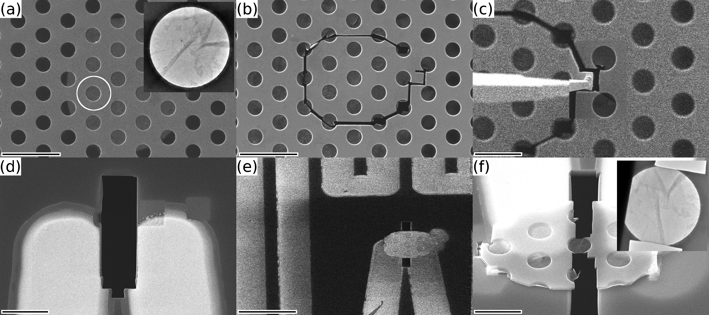
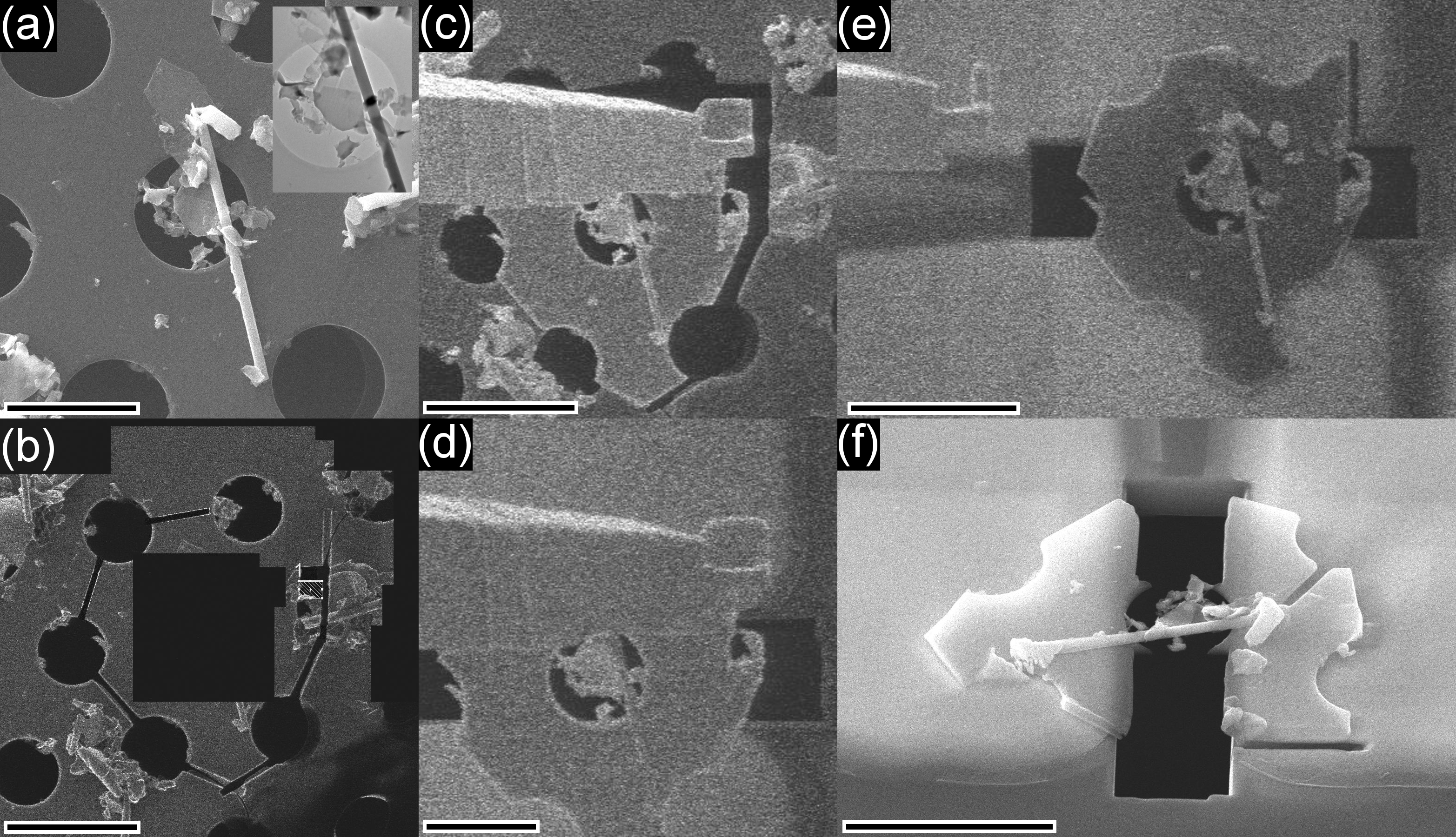
The following list details the point-by-point description of the preparation process. The example transfers in this work were performed with slight variations and the list therefore rather aims to describe the essential steps of the proposed sample preparation. Figure 1 shows six SEM or FIB images covering the major steps of the FIB part of the process for an example transfer using a GO sample. A second exemplary transfer of a NT and flake made of the MLC LaS-TaS2 is shown in Figure S1 in the supporting information.
-
1.
Thin (10-20 nm) metal coating of holey SiNx grids (C or Mo or similar metal with high melting point). Coating should be double-sided for 1D nanomaterials and for 2D nanomaterials on the opposite side of the later deposition of the film.
- 2.
-
3.
TEM analysis of sample, including electron spectroscopic techniques (EDX and EELS). Selection of nanomaterial with desired characteristics (inset in Figure 1a, Figure S1a in SI). Acquisition of a low-magnification image with location marked. Possible additional correlative microscopy techniques that can be performed on the individual nanomaterial basis.
-
4.
Location of hole with selected nanomaterial in SEM (Figure 1a) including position with respect to membrane (on top or bottom side). In this example, the film is located on the bottom side of the membrane, which is needed to avoid the insulating SiNx layer between nanomaterial and contact pad after transfer to the chip.
-
5.
Cut of SiNx membrane around the hole containing the nanomaterial by FIB (stage tilted to 52°) leaving one remaining bridge and preparation of ”landing zone” for take-out needle (Figure 1b).
-
6.
Contacting take-out needle to landing zone by Pt-FIBID with stage tilted to 0°.
-
7.
Cutting open the remaining bridge by FIB and retraction of needle with attached SiNx membrane carrying the selected nanomaterial (Figure 1c).
-
8.
Transfer of sample to in-situ chip, in which a hole has been milled previously by FIB with dimensions (between few (tens of) nm to few m) according to the selected nanomaterial and holey membrane (Figure 1d).
-
9.
Careful approach of membrane and nanomaterial to the metal contacts. Due to electrostatic charging, SiNx membrane attaches easily to the metal contact pads, leading to a decrease in contrast of the membrane when in contact (Figure S1e).
-
10.
Contacting nanomaterial or membrane to metal contacts by Pt-FIBID. As mentioned below, this is a crucial aspect as the quality of the contacts is critical for performing reliable electrical measurements, but, on the other hand, extensive FIBID inflicts contamination to the nanomaterial. In the GO example, it has been done on one side only at this point (c.f. area with bright contrast on the right side of the membrane in Figure 1e) and after the next step on the second side.
-
11.
Disconnection of landing zone with attached micro needle from rest of SiNx membrane by FIB and removal of micro needle (Figure 1e). This step can be switched with the previous one to reduce contamination of nanomaterial with the risk of a possible (partial) detachment of the SiNx membrane with nanomaterial from the in-situ chip.
-
12.
Removal of SiNx in the hole area of the in-situ chip in order that that the nanomaterial is the only connection between the contact pads (Figure 1f).
After this last step, an in-situ TEM experiment and possible correlative microscopy/spectroscopy measurements can be developed.
3.2 Avoiding damage and minimizing contamination
For the best transfer, damage and contamination of the individual nanomaterials have to be avoided. The main source of damage is a direct impact of heavy Ga+ ions on the nanomaterial. Therefore, imaging of the sample area with primary Ga+ ions has to be completely avoided in the transfer process by imaging only areas around the actual sample position using small scanning windows (see Figure S1b). To minimize damage by secondary ions created during milling or imaging of surrounding areas, FIB voltage and current should be chosen accordingly. The minimum values for both should be chosen, where sufficient imaging and milling quality is obtained. For the pre-cutting of the membrane (step 5), 16 kV yielded best results, as milling quality de- and Ga implantation increases when lowering the voltage even further. Thus, in most example transfers, we used 16 kV as well for the other steps, but, as discussed below, 5 kV was chosen for FIBID and subsequent milling processes (steps 6 & 7 and 10 & 11) for the WS2 monolayer samples to minimize contamination. Ion beam currents were smaller than 20 pA for all applications.
Contamination arises from the deposition of Pt-based precursor gases adsorbed on the nanomaterial induced by secondary electrons and ions. Secondary electrons are generated both by primary electrons and ions, so imaging with both beams in areas around the nanomaterial position has to be kept at a minimum after a FIBID/FEBID process. Imaging with the electron beam was mainly performed at 5 keV and 100 pA but the electron energy was increased to 16 keV for imaging the in-situ chip after the transfer to avoid excessive charging of its membrane.
In some experiments, we tried FEBID using 5 keV and 1.7 nA, however, FIBID has provided a higher success rate for contacting the micro-needle to the SiNx membrane at minimum dose, as the ion beam incident angle (stage at 0°) allows to directly irradiate the area between needle and membrane. The tip of the needle was thinned down to less than a m and we used a FIBID deposition window with a size of approximately 0.8x0.8 m2. For a fast and effective contacting of the micro-needle to the membrane, a conductive coating of the membrane surface has proven to be helpful, requiring the metal coating in step 1. A possible reason could be that the adhesion of the precursor gas molecules on the insulating SiNx is low.
As the precursor gases remain adsorbed on the sample for a prolonged time, even after closing the valve, imaging or milling has to be avoided for some time after the FIBID process. The factor that limits the waiting time is mechanical drift of the lift-out needle. A large drift and resulting mechanical pressure on the substrate may lead to a rupture of the membrane. To minimize this drift, the micro-needle should be driven with a small final speed (1 m/s) and let come to a rest for a few minutes close to the landing zone before contacting.
Another possible source of contamination is redeposition, which is caused during FIB milling when the material that is milled away adsorbs on areas close by. In the cutting step of the SiNx membrane before take out, the milling areas are located at a rather large distance of a few microns to the actual sample area. In step 12, when milling away the membrane on the in-situ chip, cleaning cross sections with a direction towards the sample are employed. In the performed experiments, effects derived from redeposition could not be detected (see also section 3.4).
3.3 Studied alternative approaches
Several alternative approaches were studied in this work. Initial tries to transfer nanomaterials by direct contacting to the micro-needle were not satisfactory due to stronger inevitable contamination during the FIBID/FEBID contacting processes. In addition to the SiNx support, holey TEM grids made of thick amorphous carbon and gold were tested. However, both films do not possess the mechanical stability necessary to completely avoid bending of the films during the transfer and they usually do not attach easily on the second contact pad located away from the micro needle. This may require significantly higher amount of FIBID and delicate operations with the needle.
3.4 Reference sample preparation
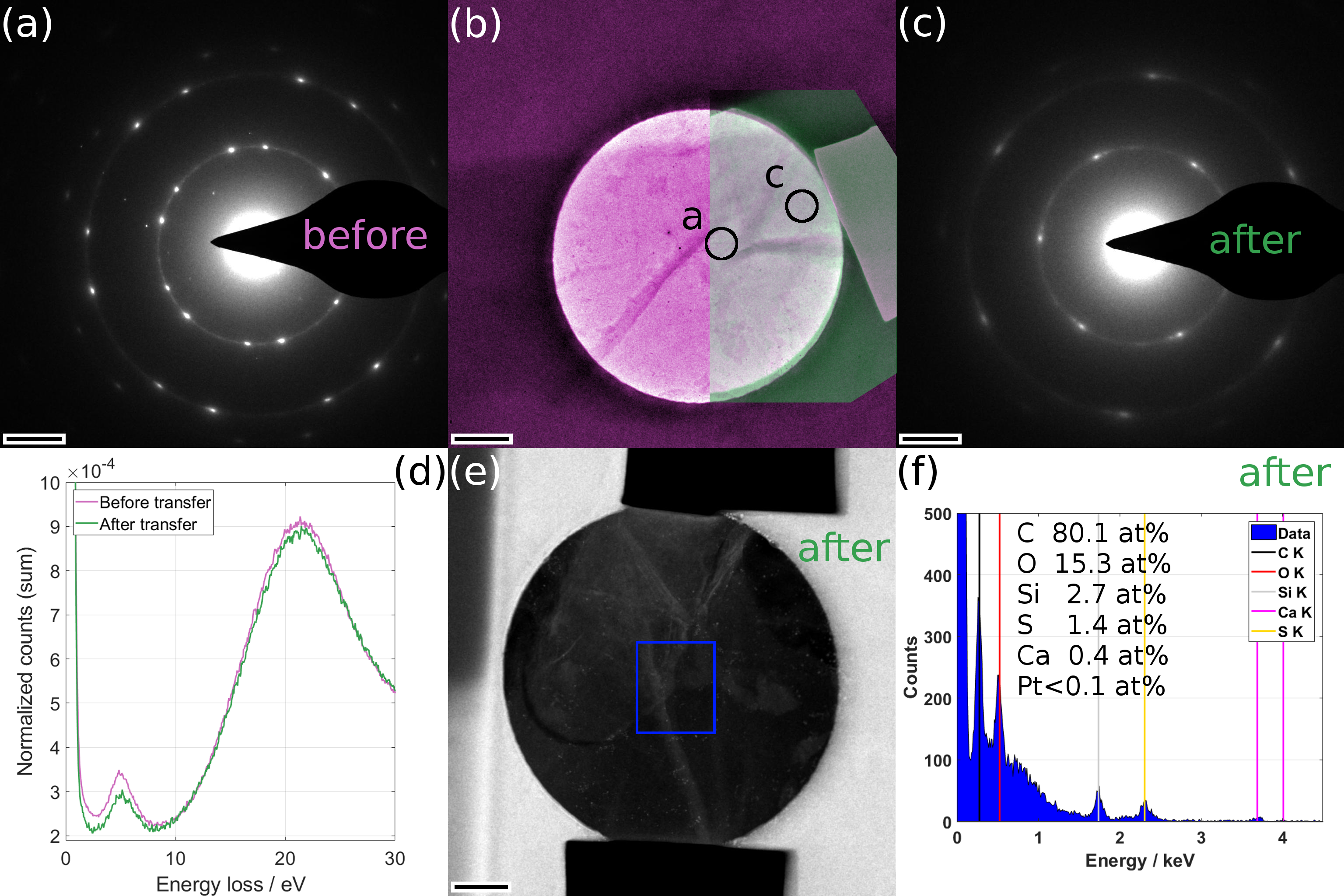
To study the impact of the sample preparation process and to establish a baseline for electrical measurements, we prepared a reference chip using a carbon-coated SiNx membrane only, i.e., without any nanomaterial. Figure 2 shows SEM images (a-d), electrical measurements (e-g) and TEM analysis (h-k) of the chip at different stages of the process. Figure 2c shows that switching points 10 (contacting of membrane to chip contacts by FIBID) and 11 (removal of needle) of the process is possible, as the SiNx membrane remains in contact with the chip after removal of the needle even without previous fixation by FIBID. A mechanical fixation is however needed before venting the SEM-FIB instrument and also required for electrical contacting (Figure 2d).
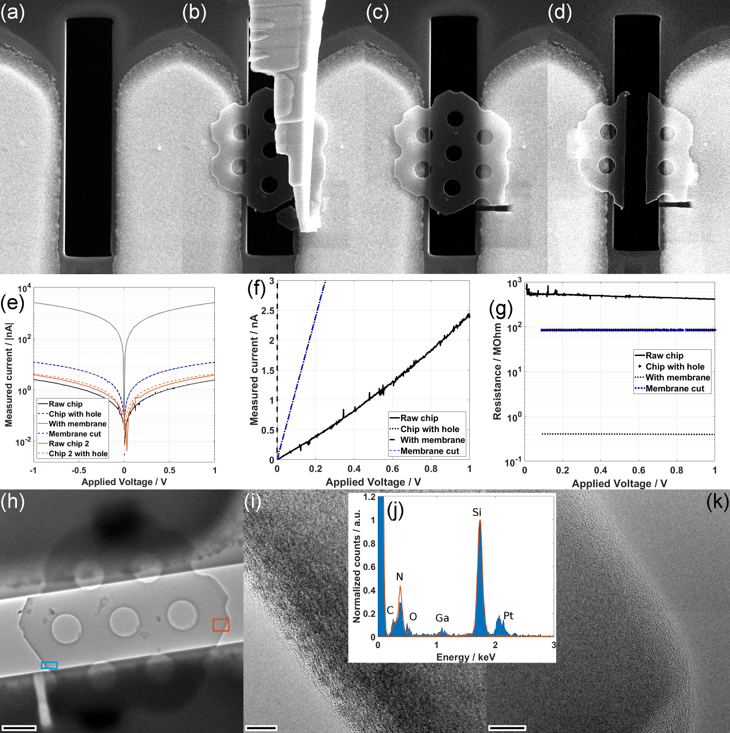
The I-V curves displayed in Figure 2e were acquired at four stages of the preparation process: (i) of the raw chip (solid line), (ii) after milling the hole between the contacts (dashed line), (iii) after transferring the membrane (dotted line) and (iv) after milling away the SiNx membrane (blue dashed line). When comparing the curves before and after milling of the hole between the contacts, an increase in current is observed, which amounts to almost one order of magnitude for chip 1 and is smaller for a second reference chip 2 (orange lines). This increase in current and related decrease in resistance (Figure 2g), is related to Ga incorporation in the SiNx membrane. The I-V curve of the untreated chip contains a non-linear component (Figure 2f), which is expected for insulating SiNx. The curve is linear after milling of the hole, consistent with a metallic behavior due to Ga presence.
A jump in current of over two orders of magnitude occurs when the C-coated SiNx membrane is transferred to the chip (Figure 2e) and the resistance decreases from 80 MOhm to 400 kOhm (Figure 2g). This shows that one can assume that only a negligible amount of the applied current will pass through the chip once a material with metallic or semiconducting behavior and a resistance below 1 MOhm is placed on the chip. The I-V curve acquired after removal of the SiNx membrane (Figure 2d) is identical to the one acquired before the transfer, proving that redeposition is negligible and is not affecting the electrical properties of the chip.
4 Evaluation of transferred samples
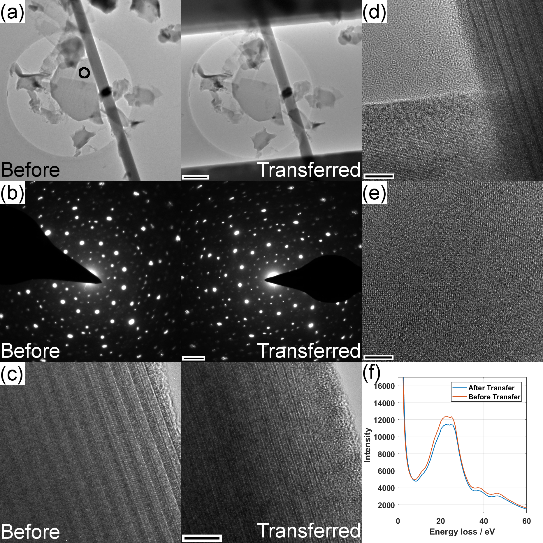
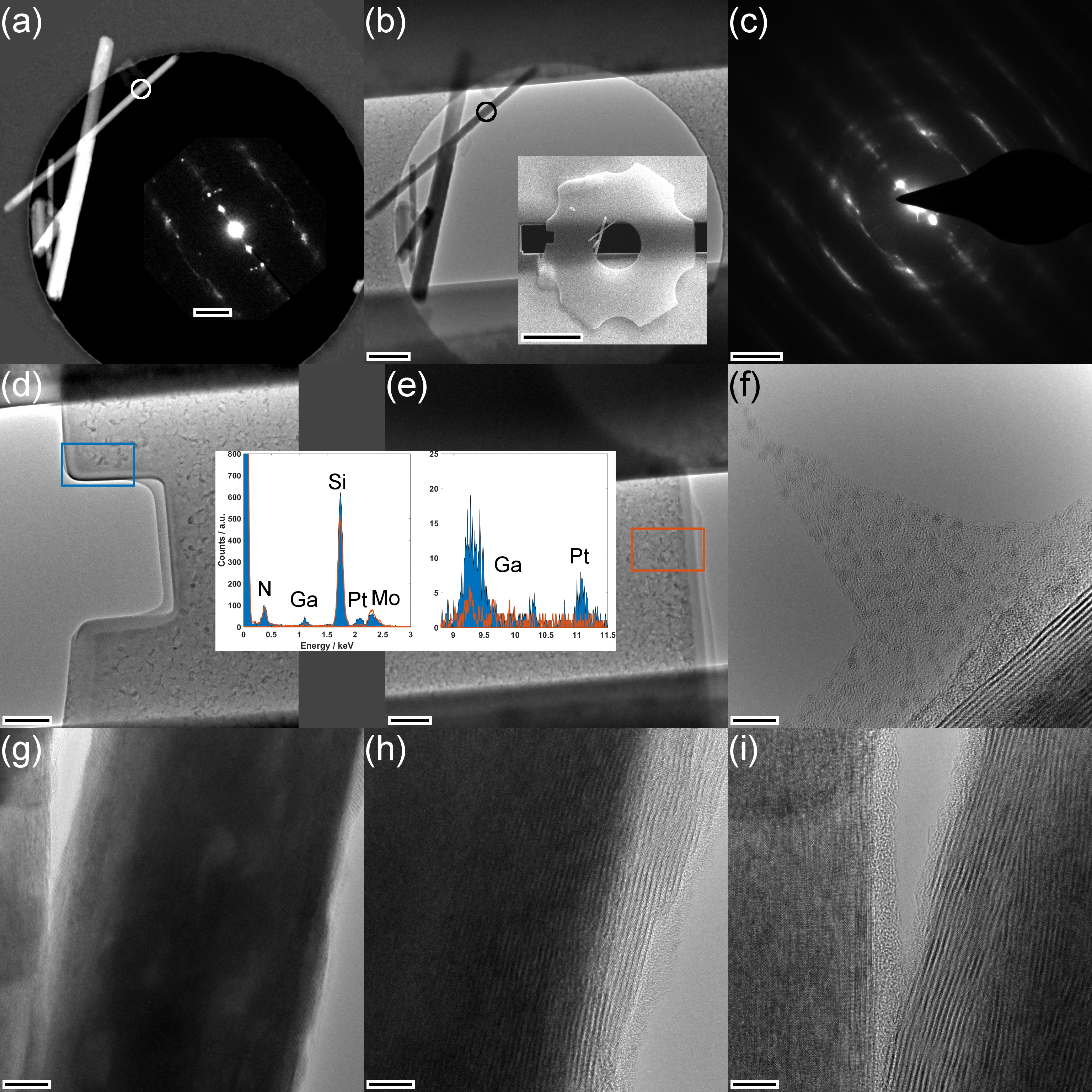
The quality of the transfer process has been evaluated for different sample transfer. First, we discuss the LaS-TaS2 NT and flake sample, whose transfer is described in Figure S1.Figure 3a-c shows a comparison of the nanomaterial before and after the transfer. In the TEM images taken at lower magnification (Figure 3a), no change induced by the transfer process is observable. On the right-hand side of Figure 3a, the edges of the hole in the in-situ chip are visible at the top and bottom of the TEM image. In Figure 3b, the fine structures of the rich selected-area electron diffraction (SAED) pattern acquired of the MLC flake as marked in (a) are preserved after the transfer.
When looking on the right border of the transferred NT, a small (less than 5 nm) amorphous deposit, which was not present before the transfer process, can be observed (Figure 3c). This amorphous contamination is attributed to the deposition of Pt-C precursor gases by secondary electrons or ions created during the FIB milling of the membrane after contacting the micro-needle to the sample and after contacting of the sample to the in-situ chip. The deposit is only observed on the right side of the NT as the FIB milling location lies to the right side of the NT (Figure S1c-e) and then, the generated secondary electrons or ions cannot easily reach the left side of the NT. The left part of the NT and the flake are therefore perfectly preserved after transfer (Figure 3d and e). Furthermore, the low-loss EEL spectrum obtained from the thin flake does not show a significant change during the transfer process (Figure 3f), with the split of the plasmon peak and the Ta-O2,3 edge clearly visible.
A comparison of the GO specimen before and after the transfer described in Figure 1 is found in the SI, Figure S2. The graphene backbone of the heterogeneous GO film is clearly preserved as shown by SAED and also morphology and even minor contamination (Si, S, Ca) is maintained perfectly during the transfer process. Pt or Ga contamination could not be found by EDX analysis after the transfer ( 0.1 at%).
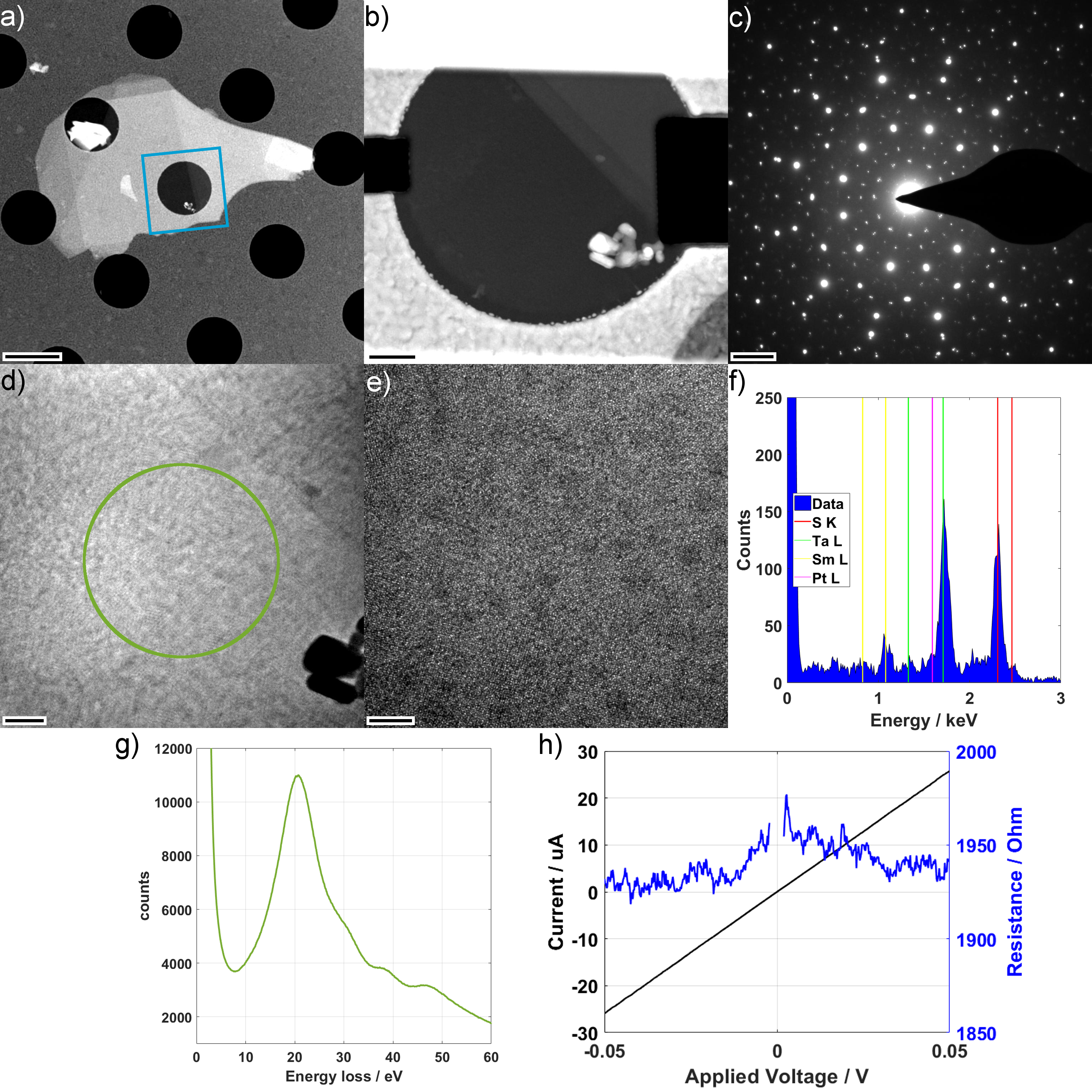
Figure S3 in the supplementary information (SI) shows the transfer evaluation of a second transferred LaS-TaS2 NT, which is as well preserved in its original state. Figure S4 shows the transfer evaluation of an inorganic 2D material, a flake made of the MLC SmS-TaS2,[24] for which we used an UltrAu support grid as sample support. As the SmS-TaS2 flake itself is mechanically very rigid, no bending of the sample during transfer was observed. This facilitated a successful contacting to the in-situ chip despite using the Au support. No modification or damage of the structure can be observed when analyzed by (S)TEM imaging, SAED and EELS. In this example, small Pt nanoparticles (5 nm) can be distinguished on the flakes’ surface and the relative amount of Pt in the flake amounts to 1 at% as determined by EDX quantification. Ideed, the actual Pt content might be less, as fluorescence signal stemming from the Pt contact pads of the in-situ chip can add to the measured Pt intensity. The total thickness of the flake is estimated to 36 nm using low-loss EELS data, the Malis formula and an average atomic number determined from EDX results.[29] Figure S4h shows an I-V characterization of the flake.
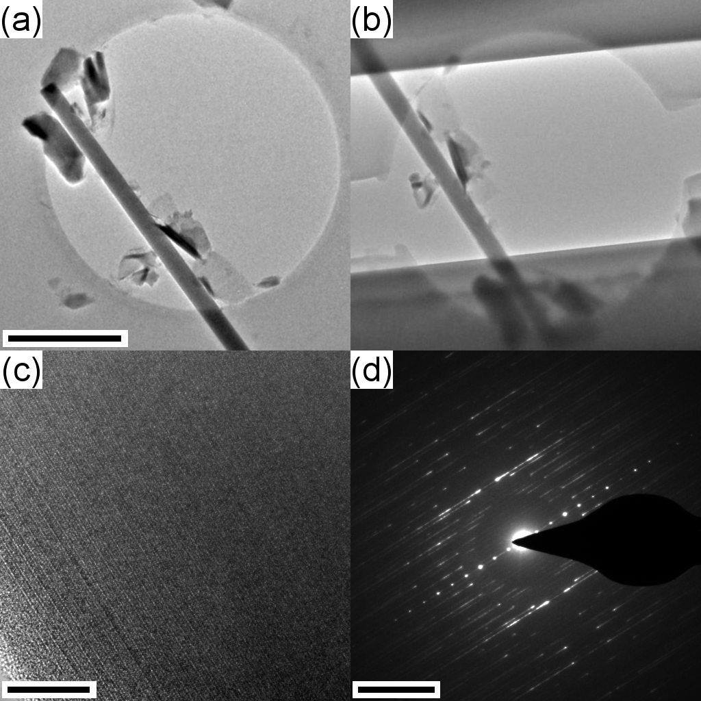
An example transfer of a WS2 NT [25] is depicted in Figure S5 showing a similar picture of a transfer without damage and with a minor Pt contamination.
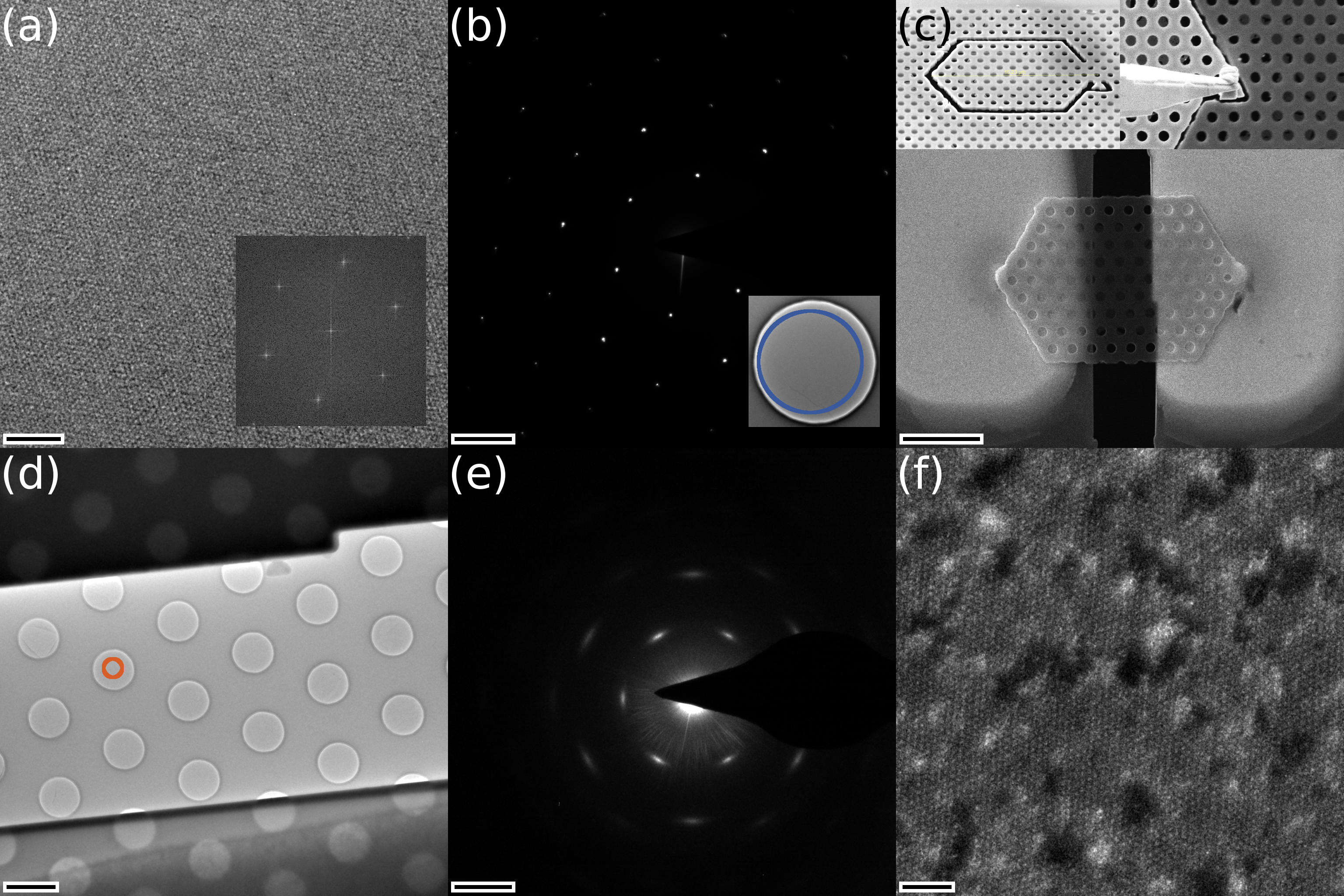
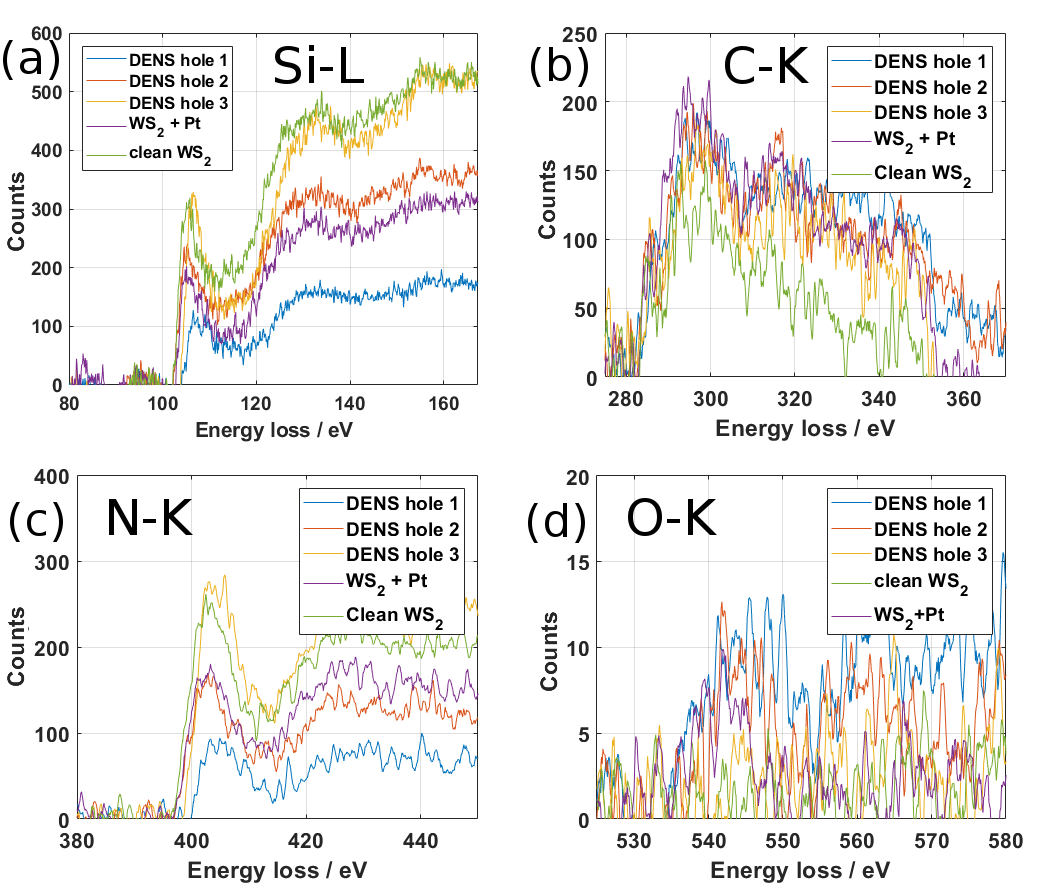
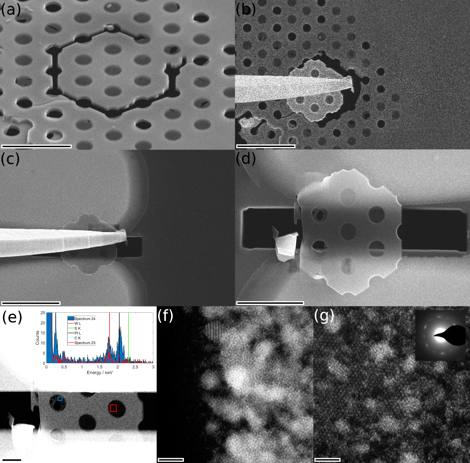
In the shown example sample transfer processes of nanomaterials, damage of the sample could not be observed and contamination is limited to a very thin amorphous Pt/C layer. For the shown larger 1D or 2D inorganic nanomaterials, this contamination is negligible allowing to study their properties by in-situ electrical TEM. To study the limits of the proposed method, we tested it to transfer a monolayer WS2 sample epitaxially grown on sapphire.[26] In a first step, the WS2 was transferred from the sapphire substrate to a SiNx TEM grid using a polystyrene-based floating approach (Figure S6).[30] Secondly, the monolayer, sustained by the SiNx holey membrane, was transferred to an in-situ chip by the method proposed in this work. The results described in Figure 4 were obtained with an operating voltage of 5 kV for the Ga ion beam for all the process steps. Figure 4a and b show a HRTEM image and a SAED pattern from the monolayer on the SiNx TEM grid after the first transfer step. Figure 4c gives an overview of the FIB-based transfer by three SEM images. Figure 4d shows a TEM image of the transferred sample revealing that, in most of the holes in the central area of the holey membrane, the film remained intact. A comparison of the SAED pattern before (b) and after (e) the transfer (not obtained on the identical sample’s area) indicates that, although the WS2 remains the largest contribution, the reflections have smeared out considerably and have also lost in intensity. This is confirmed by the HRSTEM image in Figure 4f, in which the WS2 lattice is found in the major part of the area with dark amorphous parts and brighter particles.
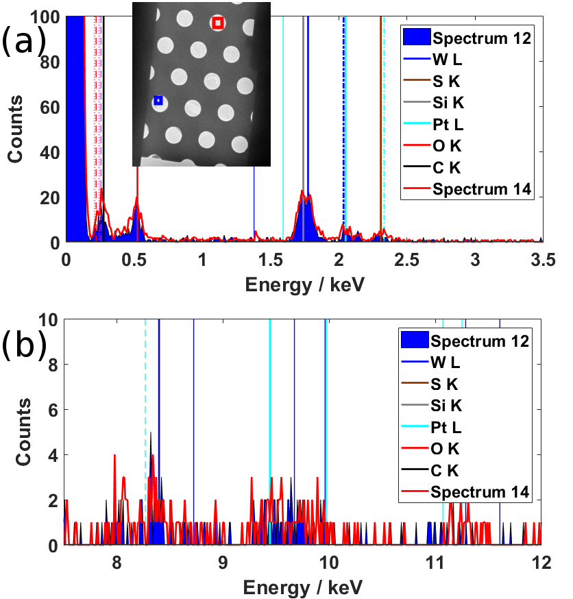
Spectroscopic analysis of the transferred sample and comparison with the WS2 sample before transfer to the in-situ chip is shown in Figure S7 and S8. After transfer, Pt is detected only in minute quantity by EDX, considerably less than W (Figure S7). As the contacts of the in-situ chip are made of Pt, the signal might be almost completely caused by fluorescence, as no Pt nanoparticles were found by STEM imaging. The EDX spectra also show the presence of Si, which is confirmed by EELS. Figure S8 shows the comparison of EEL spectra obtained from three holes of the sample described in Figure 4 with spectra from a WS2 monolayer after the first transfer step and an area with Pt contamination. Two trends are visible in the EELS results: Firstly, the Si and N contributions, related to a contamination stemming most probably from the SiNx TEM grid, are found most in the pristine sample and decrease for the areas where damage is observed. Secondly, the trend is opposite regarding C and O. This indicates that the contamination caused by the FIB-based transfer is minimum as only a small quantity of material is added. The stronger effect is related to damage, most probably caused by secondary ions, which induce a two-fold effect: an amorphisation and a removal of the SiNx contamination.
Figure S9 and S10 depict two additional sample transfers of the WS2 monolayer sample, where operating voltages of 5 and 16 kV (Figure S9) and 16 kV only (Figure S10) were employed. The results clearly show that the proposed method yields reproducible results and they also confirm that lowering the voltage of the Ga ions during and directly after the FIBID processes to 5 kV decreases the contamination on the WS2 monolayer, showing that this step is crucial to minimize damage and contamination. In contrast, the operating voltage used for the cutting of the membrane is not a critical parameter as results shown in Figure 4 and S9 are similar.
5 Preliminary in-situ TEM studies
The ability to apply electrical current to an individual nanomaterial while being able to study structure and composition at atomic resolution opens up a range of potential applications. Figure 5 summarizes several preliminary results from this area that we obtained on different materials. Besides the study the electrical properties of individual nanomaterials and linking it to their exact structure and composition, the presented preparation process allows the investigation of the electrical breakdown failure. Figure 5a shows a TEM image of a SmS-TaS2 NT after electric breakdown. A clear difference between upper and lower side at the rupture site can be distinguished indicating a large contribution from electromigration instead of a purely Joule-heating induced failure. For this sample, the SiNx membrane was coated with Pd, which formed droplets during the heating step conducted before the application of current to induce the breakdown. In the TEM image of a SmS-TaS2 flake, broken due to application of short high voltage pulses (Figure 5b, transfer shown in Figure S4), one can distinguish darker areas at the remaining edges, which were identified by EDX to be slightly deficient in S indicating a change in composition of the flake.
When using a combined in-situ chip for heating and electrical characterization, temperature-dependent effects on structure and electrical properties can be studied. Figure 5c, for example, shows the temperature-dependent I-V characterization of a NT sample, where the SiNx membrane was located between the NT and the metal contacts of the chip. The membrane acts as an insulating barrier for the electrical current, whose resistivity is strongly coupled to the sample temperature. The gradient of the I-V curves indeed increases over one magnitude when increasing the heating current from 0 (blue curve) to 5.9 mA (red curve), which translates to a decrease in resistivity of over one magnitude from 2.6 MOhm to 220 kOhm. The heating current is increased in a way to linearly increase the heating power and the temperature is estimated to increase linearly from room temperature to about 850°C. However, as we used a two-probe setting for controlling the heating device, the sample temperature can only be estimated. The I-V curves shown in Figure 5c imply that the SiNx membrane should always be located on top of the NT to facilitate a characterization of the nanomaterial without influences of an insulating barrier.
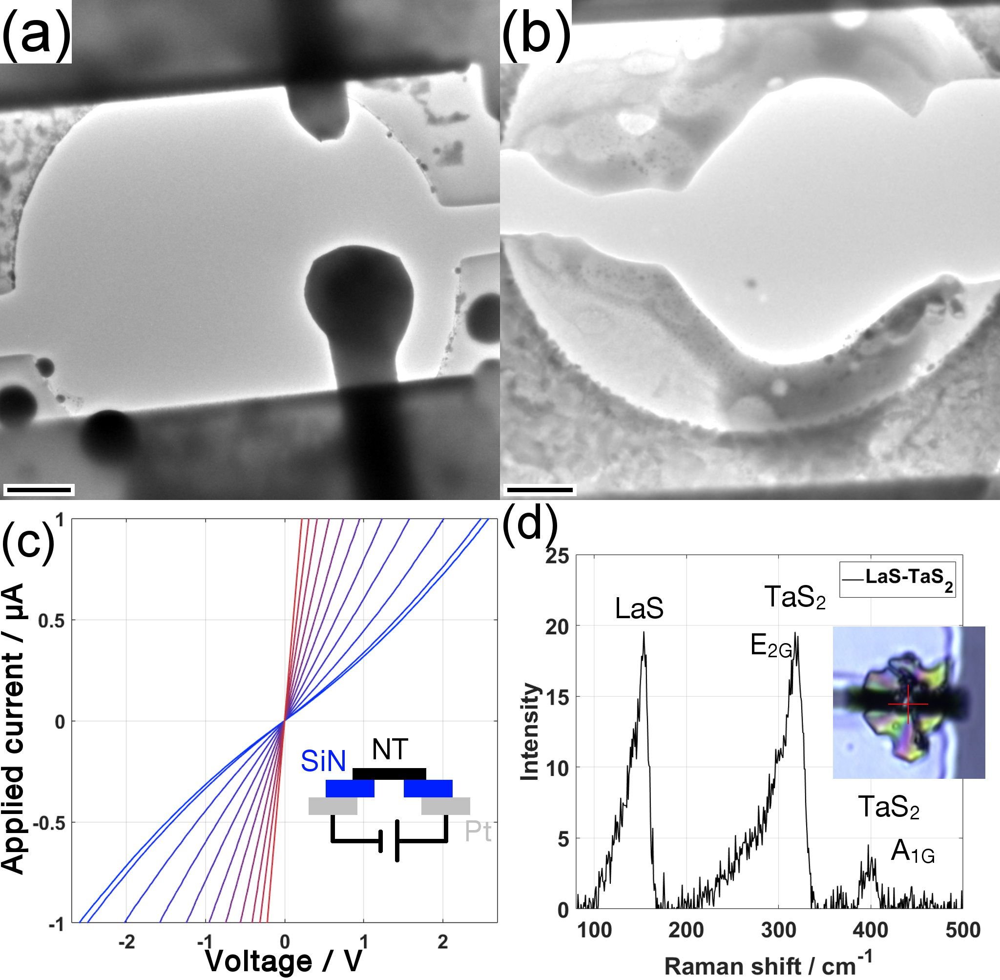
The sample transferred to the in-situ chip not only allows dedicated in-situ TEM studies but also gives the possibility to perform correlative microscopy techniques. Figure 5d shows a Raman spectrum obtained from the LaS-TaS2 sample described in Figures S1 and 3. The spectrum shows peaks in three different areas: The modes corresponding to the LaS subsystem are located between 100 and 200 cm-1 and the E2G and the A1G modes of the TaS2 lattice are found at 324 and 400 cm-1, corresponding well with literature values of this material. [23, 31].
These exemplary results illustrate the capabilities of the in-situ TEM measurements that can be performed on the transferred samples. Further detailed experiments, out of the scope of the current manuscript, will be published elsewhere with the focus on the materials’ investigations.
6 Summary and outlook
We have introduced a method facilitating and improving the transfer and contacting of individual nanomaterials to microchips with electrical contacts in a reproducible way, e.g., for electrical and/or thermal characterization by in-situ transmission electron microscopy (TEM). The benefit of using a SiNx membrane as sample support for a focused ion beam (FIB) based transfer of the nanomaterial is threefold: It firstly allows to move the necessary contacting to a lift-out needle away from the area of interest to avoid damage and minimize contamination. Secondly, it provides the mechanical stability needed to transport the nanomaterial without bending, which on its own might not possess a sufficient mechanical rigidity. Finally, it guarantees a good attachment and subsequent contacting to the metal contacts of the in-situ chip due to electrostatic charging.
With the explained process, we prepare different 1D and 2D nanomaterials, including a WS2 monolayer, with minimum damage and contamination, which is the basis for a successful in-situ experiment. Preliminary results from test experiments show that these in-situ experiments can be of different nature, including an electrical characterization linked to structure and composition at the atomic level and failure analysis upon application of electrical currents. Moreover, studies of electron-beam induced current (EBIC) or the formation of electrical current paths are possible. These studies can be combined with additional heating or possibly be performed in liquid or gas environment using specific sample holders. Moreover, further correlative microscopy and spectroscopy techniques, which allow the local analysis in the 1 m range, can be performed before and after the in-situ TEM experiments.
In addition to in-situ TEM studies, the presented transfer can be utilized to transfer nanomaterials to any other microchip that possesses electrical contacts (with or without a hole in between) and where it is not possible to synthesize the nanomaterial directly on the chip.
Acknowledgements
The authors acknowledge funding from the European Union’s Horizon 2020 research and innovation programme under the Marie Sklodowska-Curie grant agreement No 889546, by the Spanish MICINN (PID2019-104739GB-100/AEI/10.13039/501100011033 ) and from the European Union H2020 programs “ESTEEM3” (Grant number 823717). The microscopy works have been conducted in the Laboratorio de Microscopias Avanzadas (LMA) at Universidad de Zaragoza. Sample courtesy from MB Sreedhara and R. Tenne (WS2 and MLC NTs and flakes, Weizmann Institute of Science, Israel), A. Cohen and A. Ismach (WS2 monolayer, Tel Aviv University, Israel) and W. Maser and A. Benito (GO, Instituto de Carboquimica, CSIC, Zaragoza) is acknowledged. We thank I. Echañiz for support with acquisition of Raman spectra.
Supplementary information
References
-
[1]
Z. Yao, C. L. Kane, C. Dekker,
High-field electrical
transport in single-wall carbon nanotubes, Physical Review Letters 84 (13)
(2000) 2941–2944.
doi:10.1103/physrevlett.84.2941.
URL http://dx.doi.org/10.1103/PhysRevLett.84.2941 -
[2]
J.-W. Huang, C. Pan, S. Tran, B. Cheng, K. Watanabe, T. Taniguchi, C. N. Lau,
M. Bockrath, Superior
current carrying capacity of boron nitride encapsulated carbon nanotubes with
zero-dimensional contacts, Nano Letters 15 (10) (2015) 6836–6840.
doi:10.1021/acs.nanolett.5b02716.
URL http://dx.doi.org/10.1021/acs.nanolett.5b02716 -
[3]
F. M. Brunbauer, E. Bertagnolli, J. Majer, A. Lugstein,
Electrical transport
properties of single-crystal al nanowires, Nanotechnology 27 (38) (2016)
385704.
doi:10.1088/0957-4484/27/38/385704.
URL http://dx.doi.org/10.1088/0957-4484/27/38/385704 -
[4]
Z. Lin, R. Zhan, L. Li, H. Liu, S. Jia, H. Chen, S. Tang, J. She, S. Deng,
N. Xu, J. Chen,
Defect-concentration dependence
of electrical transport mechanisms in cuo nanowires, RSC Advances 8 (4)
(2018) 2188–2195.
doi:10.1039/c7ra11862g.
URL http://dx.doi.org/10.1039/C7RA11862G -
[5]
T. A. Empante, A. Martinez, M. Wurch, Y. Zhu, A. K. Geremew, K. Yamaguchi,
M. Isarraraz, S. Rumyantsev, E. J. Reed, A. A. Balandin, L. Bartels,
Low resistivity and
high breakdown current density of 10 nm diameter van der waals
tase<sub>3</sub> nanowires by
chemical vapor deposition, Nano Letters 19 (7) (2019) 4355–4361.
doi:10.1021/acs.nanolett.9b00958.
URL http://dx.doi.org/10.1021/acs.nanolett.9b00958 - [6] K. S. Roy, S. Hettler, R. Arenal, L. S. Panchakarla, Strontium-deficient sr x coo 2 –coo 2 nanotubes as a high ampacity and high conductivity material, Materials Horizons 9 (8) (2022) 2115–2127. doi:10.1039/D1MH01987B.
- [7] Y. Sato, T. Gondo, H. Miyazaki, R. Teranishi, K. Kaneko, Electron microscopy with high accuracy and precision at atomic resolution: In-situ observation of a dielectric crystal under electric field, Applied Physics Letters 111 (6) (2017) 062904. doi:10.1063/1.4986361.
- [8] Q. Zhang, X. He, J. Shi, N. Lu, H. Li, Q. Yu, Z. Zhang, L.-Q. Chen, B. Morris, Q. Xu, P. Yu, L. Gu, K. Jin, C.-W. Nan, Atomic-resolution imaging of electrically induced oxygen vacancy migration and phase transformation in srcoo2.5-s, Nature Communications 8 (1) (2017) 4791. doi:10.1038/s41467-017-00121-6.
- [9] L. Molina-Luna, S. Wang, Y. Pivak, A. Zintler, H. H. Pérez-Garza, R. G. Spruit, Q. Xu, M. Yi, B.-X. Xu, M. Acosta, Enabling nanoscale flexoelectricity at extreme temperature by tuning cation diffusion, Nature Communications 9 (1) (2018) 682. doi:10.1038/s41467-018-06959-8.
- [10] T. Ishida, H. Hiroshima, K. Higuchi, M. Tomita, K. Saitoh, T. Tanji, Development of a voltage–applicable heating specimen holder for in situ observations of solid oxide fuel cells with an environmental transmission electron microscope, Surface and Interface Analysis 52 (9) (2020) 584–590. doi:10.1002/sia.6788.
- [11] M. Arita, A. Tsurumaki-Fukuchi, Y. Takahashi, Filamentary switching of reram investigated by in-situ tem, Japanese Journal of Applied Physics 59 (SG) (2020) SG0803. doi:10.35848/1347-4065/ab709d.
- [12] P. Nukala, M. Ahmadi, Y. Wei, S. de Graaf, E. Stylianidis, T. Chakrabortty, S. Matzen, H. W. Zandbergen, A. Björling, D. Mannix, D. Carbone, B. Kooi, B. Noheda, Reversible oxygen migration and phase transitions in hafnia-based ferroelectric devices, Science 372 (6542) (2021) 630–635. doi:10.1126/science.abf3789.
- [13] S. Gorji, A. Kashiwar, L. S. Mantha, R. Kruk, R. Witte, P. Marek, H. Hahn, C. Kübel, T. Scherer, Nanowire facilitated transfer of sensitive tem samples in a fib, Ultramicroscopy 219 (2020) 113075. doi:10.1016/j.ultramic.2020.113075.
- [14] T. Kozlova, M. Rudneva, H. W. Zandbergen, In situ tem and stem studies of reversible electromigration in thin palladium–platinum bridges, Nanotechnology 24 (50) (2013) 505708. doi:10.1088/0957-4484/24/50/505708.
- [15] Martial Duchamp, Qiang Xu, Rafal E Dunin-Borkowski, Convenient preparation of high-quality specimens for annealing experiments in the transmission electron microscope, Microscopy and Microanalysis 20 (6) (2014) 1638–1645. doi:10.1017/S1431927614013476.
- [16] S. Vijayan, J. R. Jinschek, S. Kujawa, J. Greiser, M. Aindow, Focused ion beam preparation of specimens for micro-electro-mechanical system-based transmission electron microscopy heating experiments, Microscopy and Microanalysis 23 (4) (2017) 708–716. doi:10.1017/S1431927617000605.
- [17] Z. Xu, Y. Bando, L. Liu, W. Wang, X. Bai, D. Golberg, Electrical conductivity, chemistry, and bonding alternations under graphene oxide to graphene transition as revealed by in situ tem, ACS Nano 5 (6) (2011) 4401–4406. doi:10.1021/nn103200t.
- [18] S. Hettler, D. Sebastian, M. Pelaez-Fernandez, A. M. Benito, W. K. Maser, R. Arenal, In-situ reduction by joule heating and measurement of electrical conductivity of graphene oxide in a transmission electron microscope, 2D Materials 8 (3) (2021) 031001. doi:10.1088/2053-1583/abedc9.
- [19] D. Golberg, M. Mitome, K. Kurashima, C. Y. Zhi, C. C. Tang, Y. Bando, O. Lourie, In situ electrical probing and bias-mediated manipulation of dielectric nanotubes in a high-resolution transmission electron microscope, Applied Physics Letters 88 (12) (2006) 1513. doi:10.1063/1.2186987.
- [20] Z. Aslam, R. Nicholls, A. A. Koos, V. Nicolosi, N. Grobert, Investigating the structural, electronic, and chemical evolution of b-doped multi-walled carbon nanotubes as a result of joule heating, The Journal of Physical Chemistry C 115 (50) (2011) 25019–25022. doi:10.1021/jp206424v.
- [21] X. Huang, Y. Tang, C. Kübel, Di Wang, Precisely picking nanoparticles by a “nano-scalpel” for 360° electron tomography, Microscopy and Microanalysis 28 (6) (2022) 1981–1988. doi:10.1017/S1431927622012247.
- [22] L. Lajaunie, G. Radovsky, R. Tenne, R. Arenal, Quaternary chalcogenide-based misfit nanotubes lns(se)-tas(se)2 (ln = la, ce, nd, and ho): Synthesis and atomic structural studies, Inorg. Chem. 57 (2) (2018) 747–753. doi:10.1021/acs.inorgchem.7b02680.
- [23] S. Hettler, M. B. Sreedhara, M. Serra, S. S. Sinha, R. Popovitz-Biro, I. Pinkas, A. N. Enyashin, R. Tenne, R. Arenal, Ys-tas2 and yxla1-xs-tas2 (0 x 1) nanotubes: A family of misfit layered compounds, ACS Nano 14 (5) (2020) 5445–5458. doi:10.1021/acsnano.9b09284.
- [24] M. B. Sreedhara, K. Bukvišová, A. Khadiev, D. Citterberg, H. Cohen, V. Balema, A. K Pathak, D. Novikov, G. Leitus, I. Kaplan-Ashiri, M. Kolíbal, A. N. Enyashin, L. Houben, R. Tenne, Nanotubes from the misfit layered compound (sms)1.19tas2: Atomic structure, charge transfer, and electrical properties, Chemistry of materials : a publication of the American Chemical Society 34 (4) (2022) 1838–1853. doi:10.1021/acs.chemmater.1c04106.
- [25] M. B. Sreedhara, Y. Miroshnikov, K. Zheng, L. Houben, S. Hettler, R. Arenal, I. Pinkas, S. S. Sinha, I. E. Castelli, R. Tenne, Nanotubes from ternary ws2(1-x)se2x alloys: Stoichiometry modulated tunable optical properties, Journal of the American Chemical Society 144 (23) (2022) 10530–10542. doi:10.1021/jacs.2c03187.
- [26] A. Cohen, P. K. Mohapatra, S. Hettler, A. Patsha, K. V. L. V. Narayanachari, P. Shekhter, J. Cavin, J. M. Rondinelli, M. Bedzyk, O. Dieguez, R. Arenal, A. Ismach, Tungsten oxide mediated quasi-van der waals epitaxy of ws 2 on sapphire, ACS nano 17 (6) (2023) 5399–5411. doi:10.1021/acsnano.2c09754.
- [27] S. Víctor-Román, E. García-Bordejé, J. Hernández-Ferrer, J. M. González-Domínguez, A. Ansón-Casaos, A. M. T. Silva, W. K. Maser, A. M. Benito, Controlling the surface chemistry of graphene oxide: Key towards efficient zno-go photocatalysts, Catal. Today 357 (2020) 350–360. doi:10.1016/j.cattod.2019.05.049.
- [28] C. Li, A. P. Tardajos, D. Wang, D. Choukroun, K. van Daele, T. Breugelmans, S. Bals, A simple method to clean ligand contamination on tem grids, Ultramicroscopy 221 (2021) 113195. doi:10.1016/j.ultramic.2020.113195.
- [29] R. F. Egerton, Electron Energy-Loss Spectroscopy in the Electron Microscope, 3rd Edition, Springer Science+Business Media LLC, Boston, MA, 2011. doi:10.1007/978-1-4419-9583-4.
- [30] A. Gurarslan, Y. Yu, L. Su, Y. Yu, F. Suarez, S. Yao, Y. Zhu, M. Ozturk, Y. Zhang, L. Cao, Surface-energy-assisted perfect transfer of centimeter-scale monolayer and few-layer mos2 films onto arbitrary substrates, ACS nano 8 (11) (2014) 11522–11528. doi:10.1021/nn5057673.
- [31] G. Radovsky, R. Popovitz-Biro, T. Lorenz, J.-O. Joswig, G. Seifert, L. Houben, R. E. Dunin-Borkowski, R. Tenne, Tubular structures from the lns–tas 2 (ln = la, ce, nd, ho, er) and lase–tase 2 misfit layered compounds, J. Mater. Chem. C 4 (1) (2016) 89–98. doi:10.1039/C5TC02983J.