On-demand single photon emission in the telecom C-band from nanowire-based quantum dots
Abstract
Single photon sources operating on-demand at telecom wavelengths are required in fiber-based quantum secure communication technologies. In this work we demonstrate single photon emission from position-controlled nanowire quantum dots emitting at nm. Using above-band pulsed excitation, we obtain single photon purities of . These results represent an important step towards the scalable manufacture of high efficiency, high rate single photon emitters in the telecom C-band.
Long-haul terrestrial optical fiber networks operate at wavelengths in the C-band ( nm) where transmission losses are minimum. In quantum secure communications, photon loss is particularly important as it presents a loophole allowing eavesdroppers to go undetected. As such, there is currently a strong research effort to develop single photon sources operating at high rates and high efficiencies in the telecom C-bandX. Cao (2019).
Solid-state single photon emitters, and in particular, semiconductor quantum dot emittersArakawa and Holmes (2020), are a promising candidate: they offer on-demand operation at high rates and can be incorporated in photonic structures that allow for high efficiency collection. To date, quantum dots grown in both the InAs/InPMiyazawa et al. (2005); Takemoto et al. (2007, 2010); Birowosuto et al. (2012); Miyazawa et al. (2016); Müller et al. (2018); Musiał et al. (2020); Anderson et al. (2020); Musiał et al. (2021); Anderson et al. (2021); Holewa et al. (2022) and InGaAs/GaAsPaul et al. (2017); Carmesin et al. (2018); Nawrath et al. (2019); Bauer et al. (2021); Nawrath et al. (2021); Zeuner et al. (2021); Łukasz Dusanowski et al. (2022) material systems have demonstrated single photon emission in the C-band, including on-demand generationTakemoto et al. (2015); Miyazawa et al. (2016); Paul et al. (2017); Musiał et al. (2020); Nawrath et al. (2021). Current efforts are focused on establishing the indistinguishability of sequential photons emitted from such sources using two-photon interference measurements Nawrath et al. (2019, 2021); Anderson et al. (2021). The above platforms all employ quantum dots grown via Stranski-Krastanov nucleation or droplet epitaxyAnderson et al. (2021), meaning that the dots nucleate at random positions on the substrate and are, thus, difficult to scalably incorporate into devices.
In contrast, quantum dots grown by selective-area vapour-liquid-solid epitaxy (SA-VLS)Dalacu et al. (2011) are well-defined sections of a lower bandgap semiconductor surrounded by a higher bandgap nanowire. Such nanowire-based quantum dots can be incorporated in photonic structures that provide high efficiency collectionDalacu et al. (2019) and importantly, are by definition grown with position-control, offering much desired scalabilityLaferrière et al. (2022). To date, we have demonstrated single photon emission from nanowire quantum dots from wavelengths mDalacu et al. (2012) to the telecom O-bandLaferrière et al. (2023).
In this article, we extend the operating range of these site-selected single photon sources to the telecom C-band. Using above-band, pulsed excitation we obtain single photon emission at nm with a probability of multiphoton emission of . These results open possibilities for generating single photons across the C-band using structures fabricated with a scalable approach that is compatible with the silicon material systemChauvin et al. (2012).
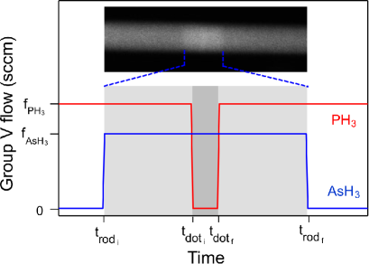
The nanowire quantum dots used in this work are based on InAsxP1-x sections in bottom-up InP nanowire cores grown using S-A VLS epitaxy, described in detail elsewhere Dalacu et al. (2011); Laferrière et al. (2022). Such structures typically operate at nm due to a low arsenic concentration of . To shift to longer wavelengths, we adopt a dot-in-a-rod structure Haffouz et al. (2020) previously used to demonstrate efficient single photon generation in the O-bandLaferrière et al. (2023). In this structure, the dot is incorporated within an InAsyP1-y rod which is embedded within the InP nanowire core. To grow these structures, we employ the switching sequence shown in Fig. 1. The rod is defined by introducing AsH3 into the growth chamber for a time whilst the dot is defined by switching off the PH3 flow for .
Four samples were grown, labelled A, B, C and D, where the growth conditions for the nanowire core were varied as shown in Table 1. Sample A was grown using the same conditions previously used to obtain O-band emission, namely the rod was grown using PH3 and AsH3 flow rates of sccm and sccm, respectively. In Samples B and C, the AsH3 flow rate was increased to sccm and sccm, respectively, whilst in D, the AsH3 flow rate was the same as in sample B but the dot growth time was increased to 6.5 seconds. In all cases the nanowire cores were clad with an InP shell to increase the total diameter of the nanowire. This diameter, , is an important parameter in designing the nanowire structures: it determines the radiative recombination lifetime of excitons in the quantum dot and for insufficiently clad nanowire cores may result in inhibited spontaneous emission ratesHaffouz et al. (2018). Here we target diameters for which nm at an emission wavelength of nm.
| Sample | ||||
|---|---|---|---|---|
| (sccm) | (sccm) | (s) | (s) | |
| A | 2 | 1 | 20 | 3.5 |
| B | 2 | 1.5 | 20 | 3.5 |
| C | 2 | 2 | 20 | 3.5 |
| D | 2 | 1.5 | 20 | 6.5 |
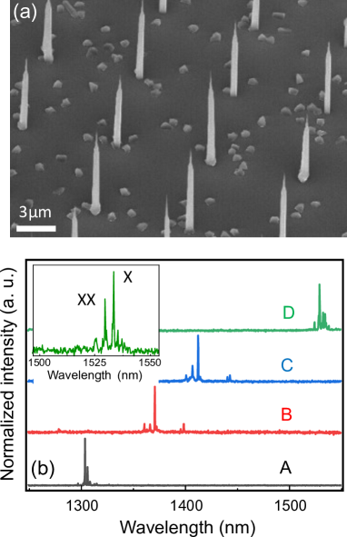
Spectrally-resolved photoluminescence (PL) measurements at 4 K were made in a closed-cycle He cryostat. Individual nanowires from a patterned array were excited above-band using continuous wave (CW) excitation at nm through a 100x cryogenic objective (numerical aperture = 0.81), see Fig. 2(a). The PL was collected through the same objective, coupled into a SMF-28 fiber and directed to a spectrometer equipped with a liquid nitrogen-cooled InGaAs linear array detector. Exemplary PL spectra of individual nanowire quantum dots from each sample, measured at excitation powers close to saturation, are shown in Fig. 2(b). Each spectrum consists of several discrete peaks, each peak corresponding to a different excitonic complex in the s-orbital of the dot. At low excitation power, we typically observe two dominant peaks (see inset) which we associate with emission from the neutral exciton, , and the biexciton .
The s-shell emission from Sample A is observed at nm, as expected from the previous studyLaferrière et al. (2023). Increasing the AsH3 flow to 1.5 sccm (Sample B) results in a redshift of 70 nm. This shift, due to a reduction in confinement from the barrier and in the dot, is a consequence of the higher arsenic concentration in the rod and dot, respectively. We note that incorporation of the rod will also increase the arsenic concentration in the dot for a given AsH3 flow by reducing memory effects in the reaction chamber i.e. the occurance of phosphorous tailing.
A further increase of the AsH3 flow to 2 sccm (Sample C) produces an additional redshift of 40 nm for an emission wavelength of nm. If, instead of reducing the confinement using composition, we simply increase the thickness of the dot (Sample D), we obtain a much larger redshift of 160 nm, (compare with Sample B) such that this sample emits at nm (i.e. in the C-band).
For this sample, we determined the diameter of the nanowire from scanning electron microscopy images, Fig. 2(a). We measured values of nm which correspond to at the emission wavelength nm i.e. significantly larger than the optimal value of Dalacu et al. (2019). For devices with such a high ratio, there will be a reduction of the total emission rate in addition to the coupling into the mode of interest, HE11, of nearly a factor of two in both cases. We also note that, unlike the optimized devices, this structure supports higher order TE01 and TM01 modes, although, this should not impact performance since an emitter on-axis of an ideal nanowire does not couple to these modes.
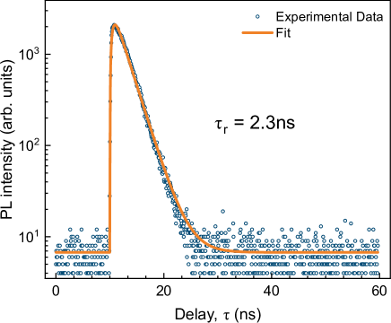
To evaluate the impact of the high ratio on the emission rate, we measured the radiative lifetime of the peak. The peak was selected using a tunable filter (bandwidth pm) and sent to a fiber-coupled superconducting nanowire single photon detector (SNSPD). Excitation was above-band ( nm) with a 100 ps pulsed laser at a repetition rate of 5 MHz. The PL decay curve, plotted in Fig. 3, shows a simple mono-exponential behaviour which we fit with an expression of the form where is an offset delay and () is the biexciton PL rise (decay) time. From the fit, we extract a radiative lifetime ns. This value is larger than that typically observed for the decay in optimized nanowire structures, consistent with the expected increase in lifetime based on the ratioXX .
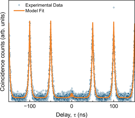
To verify the single photon purity of peak at nm we performed a second-order correlation measurement using a fiber-based Hanbury–Brown-Twiss setup. Here, the filtered emission was sent to two SNSPDs via a 50:50 fiber beamsplitter and excitation was with the nm pulsed source but with the repetition rate increased to 20 MHz. The measured coincidences, , are plotted in Fig. 4 (blue open circles) and show a significant reduction of the peak at relative to the side peaks indicative of high purity single photon emission.
The measured correlations were simulated using a stochastic model described in detail elsewhereLaferrière et al. (2020); Mnaymneh et al. (2020). In the simulation, coincidences around zero delay are attributed to a re-excitation processAichele et al. (2004); Santori et al. (2004) and modelled as a competition between the band-to-band decay rate in the barrier, the carrier capture rate into the dot, and the radiative decay rate of the exciton. We assume negligible contribution from uncorrelated emission (e.g. spectral pollution from nearby emitters) since the nanowire device contains a single quantum dot. Using the model fit (orange curve in Fig. 4) we calculate the single photon purity from the ratio of coincidences in the zero-delay peak relative to the side peaks. We obtain a raw value of which is reduced to after background subtraction.
Finally, we note that the count rates of the C-band emitter were significantly reduced, by a factor of , compared to an optimized O-band deviceLaferrière et al. (2023). This reduction was observed regardless of the type of excitation i.e. CW versus pulsed, suggesting that device efficiency rather than the transition lifetime is responsible. The lower efficiencies can result from less efficient coupling of the emitter to the fundamental waveguide mode, , due to the high ratio, as discussed above. Further, since we have increased the dot thickness to achieve C-band emission, there may be mixing of the valence ground state resulting in excitons with polarizations that do not couple to the HE11Haffouz et al. (2018). Lastly, the taper geometry of the nanowire may not be optimal for C-band emissionDalacu et al. (2021) resulting in a reduced collection efficiency of the HE11 into the external optical system. We speculate that minor modifications in the nanowire design, implemented in future growths, will produce devices with a greater than 10-fold improvement in efficiency.
In summary, we have extended our previous work on nanowire quantum dot telecom emitters to demonstrate, to our knowledge for the first time, C-band single photon emission from such structures. We measured single photon purities of at an emission wavelength of nm. Residual multi-photon emission events were attributed to re-excitation of the quantum dot from the same excitation pulse. With increased collection efficiencies and higher emission rates anticipated in optimized structures, position-controlled nanowires offer a viable route for the scalable manufacture of single photon emitters for fiber-based quantum secure communications technologies.
This work was supported by the Natural Sciences and Engineering Research Council of Canada through the Discovery Grant SNQLS, the National Research Council of Canada through the Quantum Sensing Challenge Program project ‘Telecom Photonic Resources for Quantum Sensing’ and the Canadian Space Agency through the collaborative project ‘Field Deployable Single Photon Emitters for Quantum Secured Communications’.
DATA AVAILABILITY The data that support the findings of this study are available from the corresponding author upon reasonable request.
References
- X. Cao (2019) F. D. X. Cao, M. Zopf, J. Semicond. 40, 071901 (2019).
- Arakawa and Holmes (2020) Y. Arakawa and M. J. Holmes, Appl. Phys. Rev. 7, 021309 (2020).
- Miyazawa et al. (2005) T. Miyazawa, K. Takemoto, Y. Sakuma, S. Hirose, T. Usuki, N. Yokoyama, M. Takatsu, and Y. Arakawa, J. J. Appl. Phys. 44, L620 (2005).
- Takemoto et al. (2007) K. Takemoto, M. Takatsu, S. Hirose, N. Yokoyama, Y. Sakuma, T. Usuki, T. Miyazawa, and Y. Arakawa, J. Appl. Phys. 101, 081720 (2007).
- Takemoto et al. (2010) K. Takemoto, Y. Nambu, T. Miyazawa, K. Wakui, S. Hirose, T. Usuki, M. Takutsu, N. Yokoyama, K. Yoshino, and A. Tomita, Appl. Phys. Exp. 3, 092802 (2010).
- Birowosuto et al. (2012) M. Birowosuto, H. Sumikura, S. Matsuo, H. Taniyama, P. van Veldhoven, R. Nötzel, and M. Notomi, Sci. Rep. 2, 321 (2012).
- Miyazawa et al. (2016) T. Miyazawa, K. Takemoto, Y. Nambu, S. Miki, T. Yamashita, H. Terai, M. Fujiwara, M. Sasaki, Y. Sakuma, M. Takatsu, T. Yamamoto, and Y. Arakawa, Appl. Phys. Lett. 109, 132106 (2016).
- Müller et al. (2018) T. Müller, J. Skiba-Szymanska, A. Krysa, J. Huwer, M. Felle, M. Anderson, R. Stevenson, J. Heffernan, D. Ritchie, and A. Shields, Nat. Commun. 9, 862 (2018).
- Musiał et al. (2020) A. Musiał, P. Holewa, P. Wyborski, M. Syperek, A. Kors, J. P. Reithmaier, G. Sek, and M. Benyouce, Adv. Quant. Technol. 3, 1900082 (2020).
- Anderson et al. (2020) M. Anderson, T. Müller, J. Huwer, J. Skiba-Szymanska, A. B. Krysa, R. M. Stevenson, J. Heffernan, D. A. Ritchie, and A. J. Shields, NPJ Quant. Inform. 6, 14 (2020).
- Musiał et al. (2021) A. Musiał, P. Mikulicz, A. Zielińska, P. Sitarek, P. Wyborski, M. Kuniej, J. Reithmaier, G. Sȩk, and M. Benyoucef, Appl. Phys. Lett. 118, 221101 (2021).
- Anderson et al. (2021) M. Anderson, T. Müller, J. Skiba-Szymanska, J. H. Krysa, R. M. Stevenson, J. Heffernan, D. A. Ritchie, and A. J. Shields, Appl. Phys. Lett. 118, 014003 (2021).
- Holewa et al. (2022) P. Holewa, A. Sakanas, U. M. Gür, P. Mrowiński, A. Huck, A. M. Bi-Ying Wang, K. Yvind, N. Gregersen, M. Syperek, and E. Semenova, ACS Photon. 9, 2273 (2022).
- Paul et al. (2017) M. Paul, F. Olbrich, J. Hoschele, S. Schreier, J. Kettler, S. L. Portalupi, M. Jetter, and P. Michler, Appl. Phys. Lett. 111, 033102 (2017).
- Carmesin et al. (2018) C. Carmesin, F. Olbrich, T. Mehrtens, M. Florian, S. Michael, S. Schreier, C. Nawrath, M. Paul, J. Hoschele, B. Gerken, J. Kettler, S. Portalupi, M. Jetter, P. Michler, A. Rosenauer, and F. Jahnke, Phys. Rev. B 98, 125407 (2018).
- Nawrath et al. (2019) C. Nawrath, F. Olbrich, M. Paul, S. L. Portalupi, M. Jetter, and P. Michler, Appl. Phys. Lett. 115, 023103 (2019).
- Bauer et al. (2021) S. Bauer, D. Wang, N. Hoppe, C. Nawrath, J. Fischer, N. Witz, M. Kasche, C. Schweikert, M. Jetter, S. L. Portalupi, M. Berroth, and P. Michler, Appl. Phys. Lett. 119, 211101 (2021).
- Nawrath et al. (2021) C. Nawrath, H. Vural, J. Fischer, R. Schaber, S. L. Portalupi, M. Jetter, and P. Michler, Appl. Phys. Lett. 118, 244002 (2021).
- Zeuner et al. (2021) K. Zeuner, K. D. Jöns, L. Schweickert, C. R. Hedlund, C. N. Lobato, T. Lettner, K. Wang, S. Gyger, E. Schöll, S. Steinhauer, M. Hammar, and V. Zwiller, ACS Photon. 8, 2337 (2021).
- Łukasz Dusanowski et al. (2022) Łukasz Dusanowski, C. Nawrath, S. L. Portalupi, M. Jetter, T. Huber, S. Klembt, P. Michler, and S. Höfling, Nat. Commun. 13, 748 (2022).
- Takemoto et al. (2015) K. Takemoto, Y. Nambu, T. Miyazawa, Y. Sakuma, T. Yamamoto, S. Yorozu, and Y. Arakawa, Sci. Rep. 5, 14383 (2015).
- Dalacu et al. (2011) D. Dalacu, K. Mnaymneh, X. Wu, J. Lapointe, G. C. Aers, P. J. Poole, and R. L. Williams, Appl. Phys. Lett. 98, 251101 (2011).
- Dalacu et al. (2019) D. Dalacu, P. J. Poole, and R. L. Williams, Nanotechnol. 30, 232001 (2019).
- Laferrière et al. (2022) P. Laferrière, E. Yeung, I. Miron, D. B. Northeast, S. Haffouz, J. Lapointe, M. Korkusinski, P. J. Poole, R. L. Williams, and D. Dalacu, Sci. Rep. 12, 6376 (2022).
- Dalacu et al. (2012) D. Dalacu, K. Mnaymneh, J. Lapointe, X. Wu, P. Poole, G. Bulgarini, V. Zwiller, and M. Reimer, Nano Lett. 12, 5919 (2012).
- Laferrière et al. (2023) P. Laferrière, S. Haffouz, D. B. Northeast, P. J. Poole, R. L. Williams, and D. Dalacu, Nano Lett. 23, 962 (2023).
- Chauvin et al. (2012) N. Chauvin, M. H. H. Alouane, R. Anufriev, H. Khmissi, K. Naji, G. Patriarche, C. Bru-Chevallier, and M. Gendry, Appl. Phys. Lett. 100, 011906 (2012).
- Haffouz et al. (2020) S. Haffouz, P. J. Poole, J. Jin, L. Wu, X. Ginet, K. Mnaymneh, D. Dalacu, and R. L. Williams, Appl. Phys. Lett. 117, 113102 (2020).
- Haffouz et al. (2018) S. Haffouz, K. D. Zeuner, D. Dalacu, P. J. Poole, J. Lapointe, D. Poitras, K. Mnaymneh, X. Wu, M. Couillard, M. Korkusinski, E. Schöll, K. D. Jöns, V. Zwiller, and R. L. Williams, Nano Lett. 18, 3047 (2018).
- (30) We note that the quoted decay time is for nm emitters and it is likely that this decay time is wavelength dependent. .
- Laferrière et al. (2020) P. Laferrière, E. Yeung, L. Giner, S. Haffouz, J. Lapointe, G. C. Aers, P. J. Poole, R. L. Williams, and D. Dalacu, Nano Lett. 20, 3688 (2020).
- Mnaymneh et al. (2020) K. Mnaymneh, D. Dalacu, J. McKee, J. Lapointe, S. Haffouz, J. F. Weber, D. B. Northeast, P. J. Poole, G. C. Aers, and R. L. Williams, Adv. Quant. Tech. 3, 1900021 (2020).
- Aichele et al. (2004) T. Aichele, V. Zwiller, and O. Benson, New J. Phys. 6, 90 (2004).
- Santori et al. (2004) C. Santori, D. Fattal, J. Vučković, G. S. Solomon, and Y. Yamamoto, New. J. Phys. 6, 89 (2004).
- Dalacu et al. (2021) D. Dalacu, P. J. Poole, and R. L. Williams, Nanomaterials 11, 1201 (2021).