Amorphous VOx films with high temperature coefficient of the resistivity grown by reactive e-beam evaporation of V metal
Abstract
Amorphous VOx films without a hysteretic phase transition are stable with respect to thermal cycling and highly demanded as sensitive elements of the resistive thermometers and microbolometers. In this paper we present simple and low-temperature growth of amorphous vanadium oxide films by reactive electron beam evaporation of vanadium metal in mBar oxygen atmosphere. The temperature coefficient of the resistivity (TCR) of the films is weakly sensitive to substrate material and temperature and could be tuned by oxygen pressure in the growth chamber up to -2.2% /K. The resistivity value is stable for months. It depends on the substrate material and substrate temperature during the evaporation. Simplicity and controllability of the method should lead to various laboratory and industrial applications.
I Introduction
Vanadium oxides are fascinating materials with strongly-correlated physicsKim et al. (2004) and yet puzzling phase transitionsMorin (1959); Cavalleri et al. (2004). On the other hand these materials are stableSong et al. (2017), bio-compatibleNie et al. (2014) and widely functionalHu et al. (2023). Strong temperature and deformation dependence of their properties could be used for bolometric Wang et al. (2013), thermometric Zia et al. (2017), thermochromic applications Ma et al. (2021), for strain sensorsHu et al. (2010) and actuators Liu et al. (2014).
Crystalline VO2 demonstrates structural and electronic hysteretic phase transitions at 68 ∘C with the change of crystal lattice symmetry accompanied by strong variation in conductivity and refraction coefficient. The transition temperature, hysteresis loop width and the scale of the conductivity change across the transition could be tuned by stoichiometryGriffiths and Eastwood (2003), dopingSoltani et al. (2004); Émond, Hendaoui, and Chaker (2015) and disorderRamirez et al. (2015). Importantly, the material preserves strong dependence of the physical properties on temperature even far from the transition. Phase transition leads to degradation of the films with thermal cycling and to the uncertain temperature dependence of the resistivity. From the view of electronic device fabrication it is therefore desirable to avoid the transitionAinabayev et al. (2023).
Amorphous films of VOx, where is close to 2Rehman and Dezhi (2015); Chen, Jiang, and Li (2014); Podraza et al. (2012); Venkatasubramanian et al. (2009); Petnikota et al. (2018) are well approved solutions for bolometry and thermometry Zia et al. (2017). They have strong -dependence of the resistivity without a transition. Typical values of the TCR (temperature coefficient of the resistivity) are about -2% per K in a wide range of temperatures from 0 to 100 CelsiusZia et al. (2017); Venkatasubramanian et al. (2009)).
There are many approaches to the growth of the vanadium oxide thin films, including reactive magnetron sputteringZhu et al. (2021), epitaxyAinabayev et al. (2023), pulsed laser deposition Bukhari et al. (2020), chemical vapour depositionBahlawane and Lenoble (2014), high-temperature oxidationPedrosa et al. (2016) and anodic oxidationStefanovich et al. (2004) of the vanadium films, e-beam evaporation of vanadium oxidesAryasomayajula, Reddy, and Nagendra (2008); Marvel et al. (2012); Ramana et al. (1998), spray pyrolysis Benkahoul et al. (2017); Tadeo et al. (2019), atomic layer depositionBlanquart et al. (2013). In particular, most of amorphous films reportedRehman and Dezhi (2015); Chen, Jiang, and Li (2014); Podraza et al. (2012); Venkatasubramanian et al. (2009); Petnikota et al. (2018) are fabricated by reactive magnetron sputtering.
As a rule, VOx thin film fabrication requires rather high temperatures 350-500 ∘C and/or annealing/oxidation at elevated temperatures. At such temperatures properties of vanadium oxides thin films are extremely sensitive to temperature, exposition time and oxygen concentrationBukhari et al. (2020). Therefore careful adjustment of the film preparation procedure is needed, including the process gas pressure and composition (O2/Ar ratio). Thus the reactive magnetron growth of amorphous VOx with high TCR is not a simple process.
Electron beam evaporation of metals in reactive gas atmospere is an alternative to reactive magnetron sputtering. It was shown to be an effective way to grow amorphous thin films of SnOx Behrouznejad (2023), TiOx Lin et al. (2009), AlOx and some nitrides Mencia, Lin, and Manucharyan (2021). To the best of our knowledge this approach was not previously used for VOx.
In this paper we grow amorphous VOx films with excellent properties by reactive electron beam evaporation. Vanadium metal target is used for e-beam evaporation in 10-4 mBar oxygen atmosphere, driven by continious gas flow. This route is low-temperature and very easily reproducible in almost any e-beam evaporation machine. The properties of the obtained films (TCR and resistivity value) are analogous to magnetron films and depend smoothly on three technological parameters: oxygen flow (and hence pressure), evaporation rate and substrate temperature. Optical characterization of the film (Raman, ellipsometry and transmission spectra) confirms the amorphous character and stoichiometry close to VO2. We speculate that the evaporated vanadium atoms interact with the oxygen both in the chamber during the flight and at the substrate surface. We also demonstrate compatibility of the film technology with lift-off process thus showing up the application potential.
II Methods
We grow vanadium oxide thin films using Plassys MEB-550S electron beam evaporation machine with multiple crucibles. Vanadium is evaporated from tungsten crucible. The distance between the crucible and the substrate is 0.5 m. The base vacuum of the system is 3 mBar. We add 99.9999% oxygen to the chamber using mass flow controller and measure the pressure in the range from 10-6 to mBar. For the sake of comparison we evaporate the same film thickness (mostly 30 nm) according to the the quartz monitor calibrated to vanadium. The substrate temperature could be stabilized in the range 30-700 ℃.
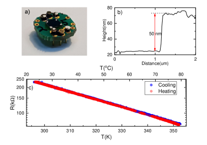
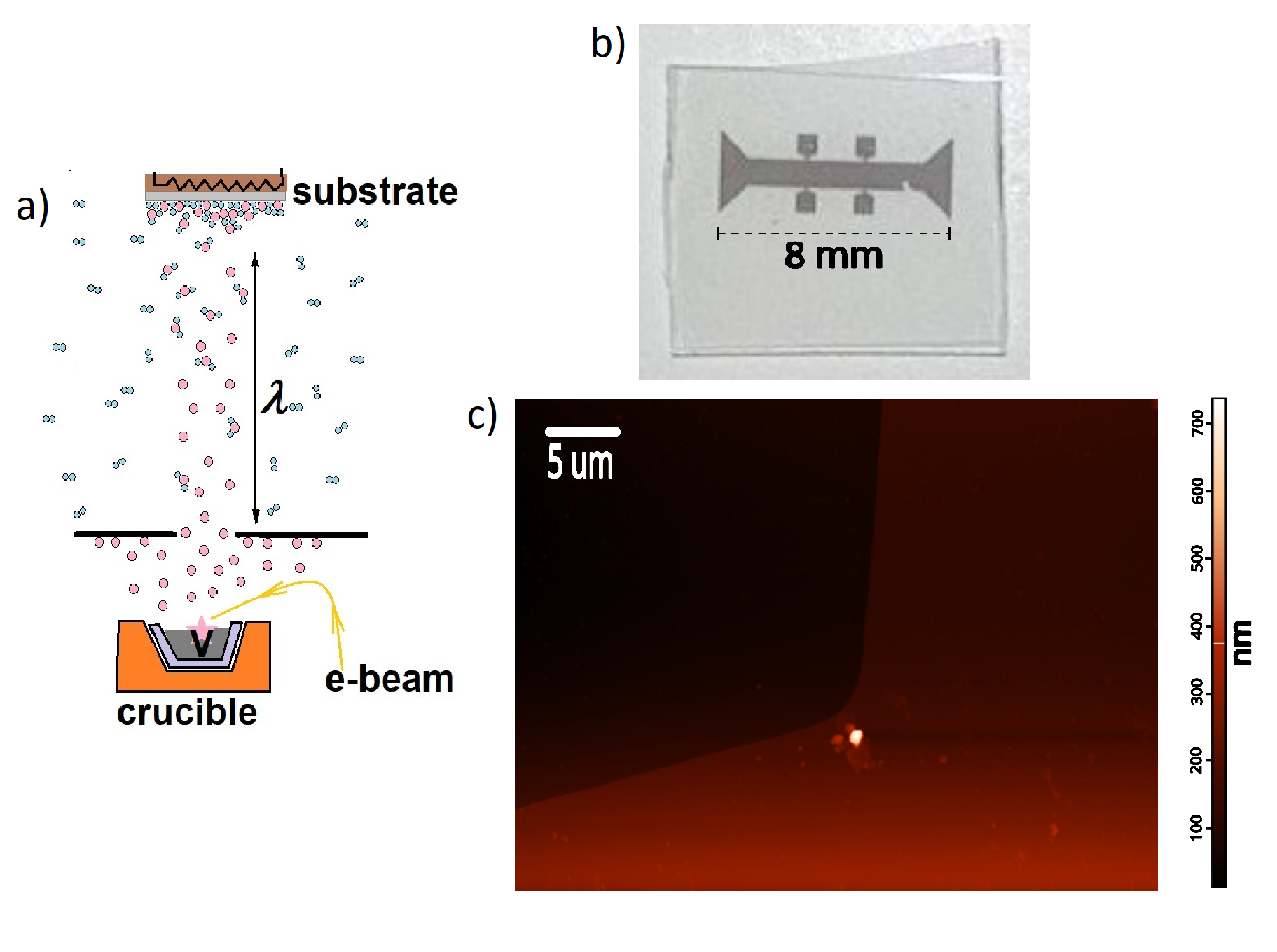
Substrate temperature, oxygen flow and evaporation rate, taken from the quartz thickness monitor are thus the growth technological parameters. The films are evaporated on different substrates (glass or sapphire). The films were characterized using atomic force microscopy in the tapping mode (Solver 47 by NT-MDT). Temperature dependence of the resistivity of the rectangular pieces in the Van der Pauw geometry was measured using home-made setup on the basis of NI 6351 data acquisition card in the range from 20 to 80 ∘C. A sample mounted for transport measurements is shown in Fig.1a. Raman spectra at 532 nm were collected using Olympus BX-51 metallographic microscope with EnSpectr R532 express analyzer.
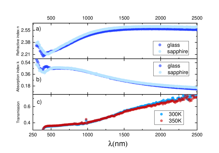
Spectral reflectance and transmittance measurements were performed over the range from 300 to 2500 nm using the J.A. Woollam VASE ellipsometer. In order to find refractive and absorption indices from the experimentally measured ellipticity parameters we model the sample as consisting of a substrate (glass or sapphire) and thin film and solve numerically the system of equations:
Here and are ellipticity parameters, is the angle of incidence, are the indices of refraction and absorption of the substrate, respectively, is the film thickness.
We chose physically plausible solution with continuous smooth spectra that satisfy the requirement .
III Results
We grew a series of thin films with the same nominal thickness (30nm) and different substrates, growth temperatures, oxygen flows and growth rates. According to AFM Fig.1b in all VOx films the real thickness is about 50 nm, that is apparently independent of the technological parameters. Raman spectra do not show up characteristic peaks. Temperature dependencies of the resistivity has no temperature hysteresis inherent to VO2, as shown in Fig.1c. All these facts together with ellipsometry measurements (see below) consistently prove the amorphous structure of the films.
The transport properties depend smoothly on the technological parameters. Let us discuss the main results:
-
1.
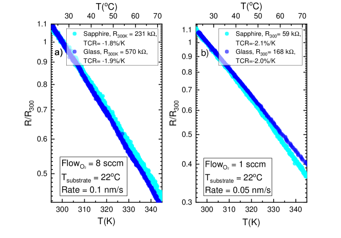
For different substrates (glass and sapphire) the TCR values for the films grown in one process are similar (Fig.2). At the same time the resistivity value for the film on glass is higher. These results are reproducible for various technological parameters (compare Fig.2a. and Fig.2b). Since the substrate holder is at room temperature and the films are amorphous, the actual temperature at the surface during the growth might be different for glass and sapphire substrates. This difference may affect the size of the VOx nanograins and the values of the resistivity in turn.
We present all results below for the sapphire substrate.
-
2.
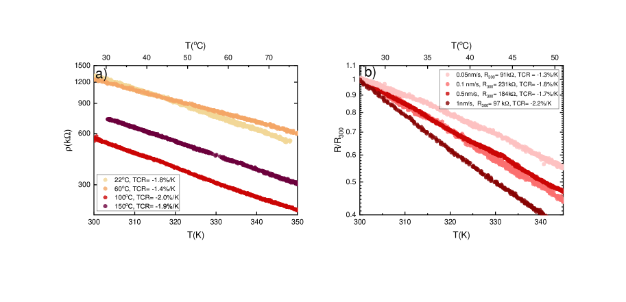
For a fixed value of oxygen flow and growth rate the resistivity of the VOx films does not depend strongly of the substrate temperature, as shown in Fig.3a: the resistivity variation is less than twofold. TCR does not demonstrate an apparent temperature dependence.
As a rule, vanadium oxides are grown at much higher substrate temperatures (above 300℃). Correspondingly, the film properties depend strongly on the substrate temperature. For example, the only paper on reactive e-beam evaporation of vanadium oxides, that we found Schuler et al. (1995), reports crystalline V2O3 films with properties strongly dependent on substrate temperature in the range 500-800 ℃.
In our work the substrate is relatively cold, therefore the oxidation threshold is mainly covered by the kinetic energy of evaporated vanadium, rather than by thermal motion energy of substrate atoms.
-
3.
For a fixed substrate temperature (22℃) and oxygen flow (8 sccm) the dependence on growth rate is related to the stoichiometry of the film (Fig.3b).
When the growth rate is low, there is excess of oxygen and the composition is shifted to V2O5: the films have higher resistivity and lower TCR. As the flow increases, the stoichiometry tends to VO2, resistivity decreases and TCR rises Walls et al. (2022). Further increase of V flow was technologically not desirable and could damage the crucible. When we attempted to grow at the maximal rate 1 nm/s and lower oxygen flow (1 sccm), a metallic-like film was formed with several tens Ohm/ resistivity and almost zero TCR.
-
4.
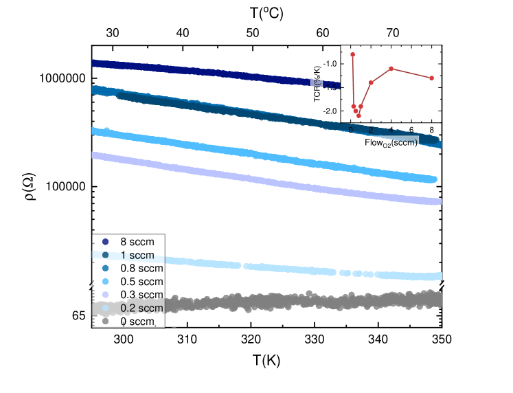
Dependence of the film resistance on oxygen flow is shown in Fig.4. The resistivity at 300K increases smoothly with oxygen flow for a fixed substrate temperature and growth rate. Pure vanadium film with 65 Ohm/ resistance is shown for the reference. An increase in film resistance with an oxygen flow corresponds to the well-known tendency in vanadium oxides Mazur et al. (2022). The non-monotonic dependence of TCR on oxygen flow was observed (see Fig.4 insert). There is a certain value of oxygen flow (1 sccm) at which TCR reaches it minimum (-2.2 %/K.), that probably corresponds to optimal stoichiometry. This TCR value is in agreement with the results obtained for magnetron-grown amorphous VOx films Rehman and Dezhi (2015); Venkatasubramanian et al. (2009). Similar films are used in commercial bolometric thermal imagers.
IV Optical measurements (Ellipsometry)
For optical measurements we grew two 80 nm thick films with the optimal growth parameters (1 sccm O2 flow, growth rate 0.05 nm/s and 22℃ substrate temperature). The optical parameter values appear to be approximately the same on both substrates (Fig.5a, Fig.5b), indicating that the substrate material does not affect the film.
V Growth mechanism
Vanadium may potentially get oxidized either on the substrate surface or during the flight in the growth chamber. The oxidation of vanadium on a substrate is well known to depend strongly on temperature. Independence of the TCR on substrate temperature suggests that essential part of the oxidation occurs on fly, as shown in the scheme of the process (Fig. 6a ).
It is useful to evaluate some figures related to the process. Mass of vanadium atom is 50 a.e.m., while oxygen molecule O2 has a mass of 32 a.e.m. Typical temperature of the evaporated vanadium atoms is about the melting temperature of vanadium 2500 K or even higher. Oxygen has room temperature 300 K. Therefore oxygen molecule has almost an order of magnitude smaller momentum than vanadium . Momentum is conserved during the collision and subsequent chemical reaction. Therefore vanadium does not deflect strongly from its trajectory. The growth rate (e.g. 0.5 nm/s ), divided by molecule volume Å3 gives the amount of V atoms per unit area and time, those achieve a substrate atoms/(cm2 s). The residual oxygen ( mbar) produces molecules hits to surface, that is atoms/(cm2 s), i.e. the flux of vanadium is smaller than the flux of oxygen. However, the probability of the chemical reaction between the cold surface and oxygen at room temperature is even smaller and the main process is on-fly oxidation.
Mean free path of vanadium atoms in the residual oxygen gas can be estimated as , where is the oxygen concentration 6 atoms/cm3, and is vanadium-oxygen scattering cross-section cm-2 (here we use vanadium atomic radius Åand oxygen molecular radius Å). Mean free path is about 0.4 m for the typical process gas pressure mbar. The distance between the electron beam source and the substrate is 0.5 m. In other words, vanadium atom with high probability meets oxygen molecule prior to achievement of a substrate. However for lower pressures mean free path is larger than substrate-to-crucible distance and the oxidation occurs at the substrate. The stoichiometry is shifted towards lower oxygen content as seen from TCR, Fig. 3.
We note that this is an oversimplified qualitative picture. In fact vanadium oxides have a tendency to form clusters up to 10 vanadium atomsAsmis and Sauer (2008). Low substrate temperature, arbitrary orientation of the clusters/ molecules and random oxidation of the V atoms does not allow forming crystalline structure of the film.
VI Discussion. Applications.
The thickness, TCR and resistivity values of our films are analogous to the reactive magnetron sputtered films from Ref. Chen, Jiang, and Li (2014). In our case however a much wider range of parameters are tested and smooth systematic dependencies of the properties are demonstrated. The main advantage of our growth method is its stability and simplicity. Vanadium metal is much easily available than vanadium oxide targets, there is also not so many requirements to stabilization of the temperature regime or gas mixture composition. Our process appeared to be so well controllable because the thermal energy of the evaporated vanadium ( K) fits well the oxidation reaction, and also because there is a long fly path where interaction with oxygen occurs. In case of magnetron sputtering many technological parameters have to be adjusted to achieve the proper energy of the V atoms and oxide formation.
The adhesion of the film to the substrate might be improved if the substrate surface is dehydrated e.g. by heating or ion bombardment. Importantly even without this preliminary procedure the adhesion is strong enough so the film survives lift-off process with standard photoresist (AZ 1512 HS). Figure 6b shows a photo of the lift-off formed mesa-stucture, and Fig. 6c shows an AFM image with a smooth edge. Lift-off process allows forming patterns without etching, that might be crucial for device fabrication. For the VOx grown at elevated temperatures this microelectronic process is impossible because the photoresist will not survive and most probably decompose. High reproducibility of the film properties in combination with lift-off process or stencil lithographyVazquez-Mena et al. (2015) may allow to pattern resistive thermometers with the pre-defined nominal resistivity on arbitrary substrates. Measurement within Hall bar geometry allowed us check that Van der Pauw value of the resistance in the same film is determined correctly. Importantly, our films did not show up any signs of degradation after 3 months of storage at ambient conditions.
Further modification of the properties is possible if the films are annealed. For example, In Ref. Venkatasubramanian et al. (2009) similar films were obtained by magnetron sputtering and then annealed.
VII Conclusions
We developed a reactive electron beam evaporation method of growth for stable amorphous VOx thin films, where . This multifunctional material is highly demanded for uncooled microbolometers and our films appeared to be similar to those grown by reactive magnetron sputtering. Compared to magnetron sputtering our process requires lower substrate temperature and is better controllable. We show experimentally and explain smooth dependence of the film properties on technological parameters.
References
- Kim et al. (2004) H.-T. Kim, B.-G. Chae, D.-H. Youn, S.-L. Maeng, G. Kim, K.-Y. Kang, and Y.-S. Lim, “Mechanism and observation of mott transition in vo2-based two- and three-terminal devices,” New Journal of Physics 6, 52 (2004).
- Morin (1959) F. J. Morin, “Oxides which show a metal-to-insulator transition at the neel temperature,” Phys. Rev. Lett. 3, 34–36 (1959).
- Cavalleri et al. (2004) A. Cavalleri, H. H. W. Chong, S. Fourmaux, T. E. Glover, P. A. Heimann, J. C. Kieffer, B. S. Mun, H. A. Padmore, and R. W. Schoenlein, “Picosecond soft x-ray absorption measurement of the photoinduced insulator-to-metal transition in ,” Phys. Rev. B 69, 153106 (2004).
- Song et al. (2017) Y. Song, T.-Y. Liu, B. Yao, T.-Y. Kou, D.-Y. Feng, X.-X. Liu, and Y. Li, “Amorphous mixed-valence vanadium oxide/exfoliated carbon cloth structure shows a record high cycling stability,” Small 13, 1700067 (2017), https://onlinelibrary.wiley.com/doi/pdf/10.1002/smll.201700067 .
- Nie et al. (2014) G. Nie, L. Zhang, J. Lei, L. Yang, Z. Zhang, X. Lu, and C. Wang, “Monocrystalline vo2 (b) nanobelts: large-scale synthesis, intrinsic peroxidase-like activity and application in biosensing,” J. Mater. Chem. A 2, 2910–2914 (2014).
- Hu et al. (2023) P. Hu, P. Hu, T. D. Vu, M. Li, S. Wang, Y. Ke, X. Zeng, L. Mai, and Y. Long, “Vanadium oxide: Phase diagrams, structures, synthesis, and applications,” Chemical Reviews 123, 4353–4415 (2023).
- Wang et al. (2013) B. Wang, J. Lai, H. Li, H. Hu, and S. Chen, “Nanostructured vanadium oxide thin film with high tcr at room temperature for microbolometer,” Infrared Physics and Technology 57, 8–13 (2013).
- Zia et al. (2017) M. F. Zia, M. Abdel-Rahman, M. Alduraibi, B. Ilahi, E. Awad, and S. Majzoub, “Electrical and infrared optical properties of vanadium oxide semiconducting thin-film thermometers,” Journal of Electronic Materials 46, 5978–5985 (2017).
- Ma et al. (2021) H. Ma, X. Xiao, Y. Wang, Y. Sun, B. Wang, X. Gao, E. Wang, K. Jiang, K. Liu, and X. Zhang, “Wafer-scale freestanding vanadium dioxide film,” Science Advances 7, eabk3438 (2021), https://www.science.org/doi/pdf/10.1126/sciadv.abk3438 .
- Hu et al. (2010) B. Hu, Y. Ding, W. Chen, D. Kulkarni, Y. Shen, V. Tsukruk, and Z. Wang, “External-strain induced insulating phase transition in vo2 nanobeam and its application as flexible strain sensor,” Advanced materials (Deerfield Beach, Fla.) 22, 5134–9 (2010).
- Liu et al. (2014) K. Liu, C. C, J. Suh, R. Tang-Kong, D. Fu, S. Lee, J. Zhou, L. Chua, and J. Wu, “Powerful, multifunctional torsional micromuscles activated by phase transition,” Advanced materials (Deerfield Beach, Fla.) 26, 1746–50 (2014).
- Griffiths and Eastwood (2003) C. H. Griffiths and H. K. Eastwood, “Influence of stoichiometry on the metal-semiconductor transition in vanadium dioxide,” Journal of Applied Physics 45, 2201–2206 (2003), https://pubs.aip.org/aip/jap/article-pdf/45/5/2201/10566252/2201_1_online.pdf .
- Soltani et al. (2004) M. Soltani, M. Chaker, E. Haddad, R. V. Kruzelecky, and J. Margot, “Effects of Ti–W codoping on the optical and electrical switching of vanadium dioxide thin films grown by a reactive pulsed laser deposition,” Applied Physics Letters 85, 1958–1960 (2004), https://pubs.aip.org/aip/apl/article-pdf/85/11/1958/13164512/1958_1_online.pdf .
- Émond, Hendaoui, and Chaker (2015) N. Émond, A. Hendaoui, and M. Chaker, “Low resistivity wxv1-xo2-based multilayer structure with high temperature coefficient of resistance for microbolometer applications,” Applied Physics Letters 107, 143507 (2015).
- Ramirez et al. (2015) J. G. Ramirez, T. Saerbeck, S. Wang, J. Trastoy, M. Malnou, J. Lesueur, J.-P. Crocombette, J. E. Villegas, and I. K. Schuller, “Effect of disorder on the metal-insulator transition of vanadium oxides: Local versus global effects,” Phys. Rev. B 91, 205123 (2015).
- Ainabayev et al. (2023) A. Ainabayev, D. Mullarkey, B. Walls, D. Caffrey, K. Zhussupbekov, A. Zhussupbekova, C. Ilhan, A. Kaisha, P. Biswas, A. Tikhonov, O. Murtagh, and I. Shvets, “Epitaxial grown vo2 with suppressed hysteresis and low room temperature resistivity for high-performance thermal sensor applications,” ACS Applied Nano Materials 6, 2917–2927 (2023).
- Rehman and Dezhi (2015) F. Rehman and S. Dezhi, “Evolution of microstructure in vanadium oxide bolometer film during annealing process,” Applied Surface Science 357, 887–891 (2015).
- Chen, Jiang, and Li (2014) R.-H. Chen, Y.-L. Jiang, and B. Li, “Influence of post-annealing on resistivity of vox thin film,” IEEE Electron Device Letters 35, 780–782 (2014).
- Podraza et al. (2012) N. J. Podraza, B. D. Gauntt, M. A. Motyka, E. C. Dickey, and M. W. Horn, “Electrical and optical properties of sputtered amorphous vanadium oxide thin films,” Journal of Applied Physics 111, 073522 (2012), https://pubs.aip.org/aip/jap/article-pdf/doi/10.1063/1.3702451/15085237/073522_1_online.pdf .
- Venkatasubramanian et al. (2009) C. Venkatasubramanian, O. M. Cabarcos, D. L. Allara, M. W. Horn, and S. Ashok, “Correlation of temperature response and structure of annealed VOx thin films for IR detector applications,” Journal of Vacuum Science and Technology A 27, 956–961 (2009), https://pubs.aip.org/avs/jva/article-pdf/27/4/956/13302659/956_1_online.pdf .
- Petnikota et al. (2018) S. Petnikota, R. Chua, Y. Zhou, E. Edison, and M. Srinivasan, “Amorphous vanadium oxide thin films as stable performing cathodes of lithium and sodium-ion batteries,” Nanoscale Research Letters 13, 363 (2018).
- Zhu et al. (2021) M. Zhu, D. Zhang, S. Jiang, S. Liu, H. Qi, and Y. Yang, “Phase evolution and thermochromism of vanadium oxide thin films grown at low substrate temperatures during magnetron sputtering,” Ceramics International 47 (2021), 10.1016/j.ceramint.2021.02.115.
- Bukhari et al. (2020) S. A. Bukhari, S. Kumar, P. Kumar, S. P. Gumfekar, H.-J. Chung, T. Thundat, and A. Goswami, “The effect of oxygen flow rate on metal-insulator transition (MIT) characteristics of vanadium dioxide (VO2) thin films by pulsed laser deposition (PLD),” Applied Surface Science 529, 146995 (2020).
- Bahlawane and Lenoble (2014) N. Bahlawane and D. Lenoble, “Vanadium oxide compounds: Structure, properties, and growth from the gas phase,” Chemical Vapor Deposition 20 (2014), 10.1002/cvde.201400057.
- Pedrosa et al. (2016) P. Pedrosa, N. Martin, R. Salut, M. Arab Pour Yazdi, and A. Billard, “Controlled thermal oxidation of nanostructured vanadium thin films,” Materials Letters 174 (2016), 10.1016/j.matlet.2016.03.097.
- Stefanovich et al. (2004) G. Stefanovich, A. Pergament, A. Velichko, and L. Stefanovich, “Anodic oxidation of vanadium and properties of vanadium oxide films,” Journal of Physics: Condensed Matter 16, 4013 (2004).
- Aryasomayajula, Reddy, and Nagendra (2008) S. Aryasomayajula, Y. Reddy, and C. Nagendra, “Nano-vanadium oxide thin films in mixed phase for microbolometer applications,” Journal of Physics D: Applied Physics 41, 195108 (2008).
- Marvel et al. (2012) R. Marvel, K. Appavoo, B. Choi, J. Nag, and R. Haglund, “Electron-beam deposition of vanadium dioxide thin films,” Applied Physics A , 1–7 (2012).
- Ramana et al. (1998) C. V. Ramana, O. M. Hussain, S. Uthanna, and B. Srinivasulu Naidu, “Influence of oxygen partial pressure on the optical properties of electron beam evaporated vanadium pentoxide thin films,” Optical Materials 10, 101–107 (1998).
- Benkahoul et al. (2017) M. Benkahoul, M. Zayed, A. Solieman, and S. N. Alamri, “Spray deposition of v4o9 and v2o5 thin films and post-annealing formation of thermochromic vo2,” Journal of Alloys and Compounds 704 (2017), 10.1016/j.jallcom.2017.02.088.
- Tadeo et al. (2019) I. Tadeo, M. Panzi, S. Krupanidhi, and A. Umarji, “Low-cost vo2 (m1) thin films synthesized by ultrasonic nebulized spray pyrolysis of an aqueous combustion mixture for ir photodetection,” RSC Advances 9, 9983–9992 (2019).
- Blanquart et al. (2013) T. Blanquart, J. Niinistö, M. Gavagnin, V. Longo, M. Heikkilä, E. Puukilainen, V. Pallem, C. Dussarrat, M. Ritala, and M. Leskelä, “Atomic layer deposition and characterization of vanadium oxide thin films,” RSC Advances 3, 1179–1185 (2013).
- Behrouznejad (2023) F. Behrouznejad, “Reactive e-beam evaporated snox layer as an effective etl for highly efficient spray-coated perovskite solar cells,” Materials Chemistry and Physics 306, 128086 (2023).
- Lin et al. (2009) Z. Lin, I.-S. Lee, Y.-J. Choi, I.-S. Noh, and S.-M. Chung, “Characterizations of the tio2-x films synthesized by e-beam evaporation for endovascular applications,” Biomedical materials (Bristol, England) 4, 015013 (2009).
- Mencia, Lin, and Manucharyan (2021) R. Mencia, Y.-H. Lin, and V. Manucharyan, “Superconducting titanium nitride films grown by directional reactive evaporation,” Journal of Applied Physics 130, 225109 (2021), https://pubs.aip.org/aip/jap/article-pdf/doi/10.1063/5.0048819/15273893/225109_1_online.pdf .
- Schuler et al. (1995) H. Schuler, G. Weissmann, C. Renner, S. Six, S. Klimm, F. Simmet, and S. Horn, “Effect of growth conditions and buffer layers on the metal-insulator transition in v2o3 thin films,” MRS Online Proceedings Library 401, 61–66 (1995).
- Walls et al. (2022) B. Walls, O. Murtagh, S. I. Bozhko, A. Ionov, A. A. Mazilkin, D. Mullarkey, A. Zhussupbekova, D. A. Shulyatev, K. Zhussupbekov, N. Andreev, N. Tabachkova, and I. V. Shvets, “Vox phase mixture of reduced single crystalline v2o5: Vo2 resistive switching,” Materials 15 (2022), 10.3390/ma15217652.
- Mazur et al. (2022) M. Mazur, A. Lubańska, J. Domaradzki, and D. Wojcieszak, “Complex research on amorphous vanadium oxide thin films deposited by gas impulse magnetron sputtering,” Applied Sciences 12 (2022), 10.3390/app12188966.
- Van Bilzen et al. (2015) B. Van Bilzen, P. Homm, L. Dillemans, C.-Y. Su, M. Menghini, M. Sousa, C. Marchiori, L. Zhang, J. W. Seo, and J.-P. Locquet, “Production of vo2 thin films through post-deposition annealing of v2o3 and vox films,” Thin Solid Films 591, 143–148 (2015).
- Asmis and Sauer (2008) K. Asmis and J. Sauer, “Erratum: Mass-selective vibrational spectroscopy of vanadium oxide cluster ions (mass spectrometry reviews (2007) 26 (542-562)),” 27 (2008), 10.1002/mas.20163.
- Vazquez-Mena et al. (2015) O. Vazquez-Mena, L. Gross, X. Shenqi, L. G. Villanueva, and J. Brugger, “Resistless nanofabrication by stencil lithography: A review,” Microelectronic Engineering 132, 236–254 (2015).