3D Topological Semimetal Phases of Strained -Sn on Insulating Substrate
Abstract
-Sn is an elemental topological material, whose topological phases can be tuned by strain and magnetic field. Such tunability offers a substantial potential for topological electronics. However, InSb substrates, commonly used to stabilize -Sn allotrope, suffer from parallel conduction, restricting transport investigations and potential applications. Here, the successful MBE growth of high-quality -Sn layers on insulating, hybrid CdTe/GaAs(001) substrates, with bulk electron mobility approaching 20000 cm2V-1s-1 is reported. The electronic properties of the samples are systematically investigated by independent complementary techniques, enabling thorough characterization of the 3D Dirac (DSM) and Weyl (WSM) semimetal phases induced by the strains and magnetic field, respectively. Magneto-optical experiments, corroborated with band structure modeling, provide an exhaustive description of the bulk states in the DSM phase. The modeled electronic structure is directly observed in angle-resolved photoemission spectroscopy, which reveals linearly dispersing bands near the Fermi level. The first detailed study of negative longitudinal magnetoresistance relates this effect to the chiral anomaly and, consequently, to the presence of WSM. Observation of the Berry phase in Shubnikov-de Haas oscillations agrees with the topologically non-trivial nature of the investigated samples. Our findings establish -Sn as an attractive topological material for exploring relativistic physics and future applications.
1 Introduction
Tin is a well-known functional material that has two allotropes stable in near-ambient conditions. Above \qty13.2, it exits in metallic form with a tetragonal crystal structure known as -Sn or white tin. It is an industrially important material widely used in soldering alloys [1], which has recently been proposed as a promising superconductor for fault-tolerant quantum computing [2, 3, 4]. Below \qty13.2, -Sn transforms into diamond-cubic form known as -Sn or grey tin. This low-temperature allotrope is attracting increasing attention of the scientific community after it was predicted to be a rare example of elemental topological material [5, 6, 7], with possible applications in spin-to-charge conversion [8, 9], spin-orbit torque devices [10, 11] and as an anode for high efficient Na-based ion batteries [12]. The promise of lower disorder, higher purity and lack of defects related to non-perfect stoichiometry compared to compounds and alloys makes grey tin an attractive material for topological electronics [13, 14]. Even both allotropes can be combined in a single electronic device showing a giant superconducting diode effect promising for superconducting spintronics [15].
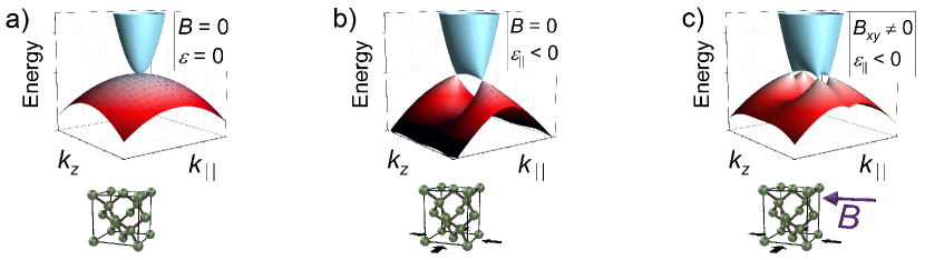
In its bulk form, -Sn is a zero-gap semiconductor with a diamond crystal structure [16, 17] and degenerate bands (see Figure 1a). The degeneracy of these heavy- and light-hole (HH and LH, respectively) bands at the point of the Brillouin zone is protected by the crystal lattice symmetry. Breaking of this symmetry, for example, by external strain, leads either to the opening of the energy gap or to the crossing of the conduction and valence bands [18, 6, 19]. It may result in the formation of different topological phases, including topological insulator (TI) and Dirac semimetal (DSM), due to the inversion that occurs between the bands and band (S band) located at lower energy [5, 6, 7]. In particular, as presented schematically in Figure 1b, a tetragonal distortion (compressive biaxial strain associated with tensile uniaxial strain) transforms -Sn into DSM, with two Dirac cones formed along out-of-plane k vector. The application of an external magnetic field breaks the time reversal symmetry (TRS) and leads to the splitting of each of the Dirac cones into a pair of Weyl cones - a Weyl semimetal (WSM) is formed, as shown in Figure 1c. Control over electronic properties of -Sn can also be realized by reduction of the sample’s thickness: below some critical value, the TI phase is formed regardless of strain [20]. Further reduction of thickness to several monolayers leads to the formation of the buckled phase of -Sn called stanene [21] known by its superconducting [22, 23] and other intriguing characteristics [24]. In addition to the potential spintronic applications, such a multitude of possible phases makes -Sn a convenient topological playground for studying relativistic physics in a simple solid state system due to the so-called relativistic analogy [25].
Experimental studies of -Sn are hindered by its low stability at room temperature [26]. This limitation can be overcome by the fabrication of thin layers, e.g. by molecular beam epitaxy (MBE). The lattice-matched substrate can stabilize the crystal structure of grey tin [27], enabling room-temperature sample characterization and processing. The common choices for the substrates are nearly lattice-matched CdTe and InSb [27]. Both introduce a small biaxial compressive strain in -Sn layers, paving the way for the engineering of the topological phases in this material. The topologically non-trivial character of grey tin grown on InSb was confirmed by extensive angle-resolved photoemission spectroscopy (ARPES) [28, 29, 8, 19, 30, 31, 32, 33, 34, 35]. The main focus of those reports was on the characterization of 2D topological surface states, leaving bulk bands of DSM phase weekly explored [19, 35]. Additionally, intrinsically doped InSb creates a parallel conduction channel and makes it difficult to extract properties of -Sn from magneto-transport measurements [32, 36, 37, 38, 39]. The recent attempts to grow on an insulating CdTe suffered from the lower surface quality of the substrate and resulted in reduced carrier mobility of -Sn [40, 41]. Further improvement was received by inserting a thin conducting InSb interlayer between -Sn and an insulating CdTe substrate [39]. To the best of our knowledge, no systematic experimental investigation of the band structure and magneto-transport properties of -Sn grown directly on an insulating substrate has been conducted so far.
In this report, we demonstrate the reproducible MBE growth of -Sn on hybrid CdTe/GaAs(001) substrates. The fabrication of CdTe on GaAs is well-established [42, 43, 44] and allows to obtain high-quality heterostructures exhibiting quantum Hall effect [43]. Therefore, we can simultaneously take advantage of the insulating character of the substrates and of the enhanced surface quality of the CdTe/GaAs structure. By expanding the thickness range of the films up to \qty200\nano, well above the critical value for the transition to the TI phase, we were able to provide the first comprehensive characterization of the bulk Dirac fermions in this material. The diversity of applied experimental techniques allows us to extract a number of band- and material parameters. It results in a self-consistent description of -Sn in agreement with the predicted DSM and WSM phases. The high quality of the grown samples is confirmed by transmission electron microscopy (TEM) and X-ray diffraction (XRD), which also provide evidence of the presence of the in-plane compressive strain (subsection 2.1). Magneto-optical studies yield a set of band structure parameters for the 4-band Hamiltonian (subsection 2.2), which, together with the value of the strain determined by XRD, describes the bulk bands in agreement with the expected DSM phase. Modelled band structure, accompanied by a set of surface states, is observed in ARPES (subsection 2.3). The insulating character of the hybrid substrates used for epitaxy allowed us to perform the first systematic magneto-transport studies of -Sn and, particularly, to observe negative longitudinal magnetoresistance (NLMR). By ruling out alternative sources, we are able to relate this feature to the chiral anomaly - a signature of the WSM [45, 46, 47], in agreement with earlier prediction [6] (subsection 2.4). Analysis of SdH oscillations clearly shows a -Berry phase and a 3D nature of the carriers (subsection 2.4), in consistency with the rest of the obtained results.
2 Results and discussion
2.1 MBE growth and structural characterization
Layers of -Sn in the thickness range of \qtyrange30200\nano were grown by molecular beam epitaxy (MBE) on (001) GaAs substrates with CdTe buffer ( thick); details of growth are given in the section 4. The quality of the CdTe buffer obtained in the present work was monitored in-situ by reflection high-energy electron diffraction (RHEED), which showed sharp, streaky reflections on Laue semicircle and intense Kikuchi lines - evidence of a smooth single-crystalline surface (see Figure 2a). A similar RHEED pattern was obtained for the Sn epilayers subsequently grown on fresh CdTe (Figure 2b). Atomic force microscopy (AFM) of the Sn films also shows a smooth surface with root mean square (RMS) roughness on the order of \qty2\nano (Figure 2c), resulting from the roughness of the underlying CdTe buffer. X-ray diffraction (XRD) scans confirm the presence of the phase of Sn. Only {001} maxima are present, with (004) and (008) reflections of Sn clearly visible and (002) and (006) reflections fully suppressed, as expected for the structural factor of diamond crystal structure (Figure 2d-f). The smoothness of the -Sn/CdTe interface and of the film surface is further confirmed by the presence of a large number of thickness fringes in the HR-XRD pattern obtained for thin (\qtyrange3050\nano) layers (Figure 2e).
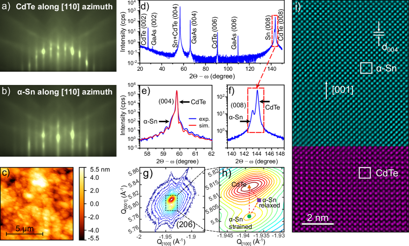
The small lattice mismatch between -Sn and CdTe () is expected to introduce biaxial in-plane compressive strain in the MBE-grown layers. Its presence is confirmed by the X-ray reciprocal space maps (RSM) of asymmetric (206) (Figure 2g, h) and (115) reflections. The epilayers were found to be fully strained, regardless of their thickness, with an in-plane lattice constant equal to that of the CdTe buffer, . Such in-plane bi-axial compressive strains induce uniaxial out-of-plane strain (). The values of the unstained lattice constant , as well as the in-plane and out-of-plane strains ( and , respectively) were calculated using elastic constants of the bulk -Sn [48] (see Table 1). The obtained value of agrees with the previous reports, and the amount of strains is similar to that in -Sn grown on InSb [27, 19, 49, 50, 51, 35, 52].
The structural quality of the obtained samples is further confirmed by high-resolution scanning transmission electron microscopy (HR-STEM) (see Figure 2i). It showed a homogeneous epitaxial -Sn layer with a smooth -Sn/CdTe interface, characterized by the absence of mismatch dislocations. The absence of cracks in the volume of the layer suggests uniform strain distribution, even in 200 nm thick films. Importantly, neither the XRD nor the TEM studies revealed the presence of -Sn inclusions. Observed tetragonal distortion in -Sn induced by compressive in-plane strains is a prerequisite for the formation of the DSM and WSM phases [6, 7]. We note that despite the room-temperature characterization, we expect the same amount of strains at lower temperatures due to similar thermal expansion of the film, buffer, and substrate [51, 53, 54].
| Material | Reflection | [Å] | [Å] | [Å] | [%] | [%] |
|---|---|---|---|---|---|---|
| Sn | (206) | 6.481 | 6.497 | 6.490 | -0.14 | 0.12 |
| CdTe | (206) | 6.481 | 6.484 | 6.4822 | -0.02 | 0.02 |
| Sn | (115) | 6.481 | 6.498 | 6.490 | -0.14 | 0.12 |
| CdTe | (115) | 6.481 | 6.484 | 6.4823 | -0.02 | 0.03 |
2.2 Model of the band structure and magneto-optical studies
The bulk band structure of -Sn close to the point, presented schematically in Figure 1, can be described by the kp model based on Pidgeon-Brown [55, 56] and Bir-Pikus [57, 58] Hamiltonians. Details of the model can be found in the Supporting Information (SI). The Pidgeon-Brown Hamiltonian depicts the eight bands that are close to the Fermi energy and to the -point of a bulk -Sn while taking the remote bands effects up to the second order in . The resulting modelled band structure consists of four bands that are twofold spin degenerate: the split-off (P) band, the heavy hole (HH) band, the light hole (LH) band, and the s-type (S) band, whose energies at , before taking the strain into account, are , 0, 0, and , respectively. The interaction between the s-type band and the other three p-type bands is defined by the interband momentum matrix element , where is the electron velocity. Remote band effects are described by the parameters and that account for a parabolic correction to the effective masses of the LH and HH bands. A non-zero magnetic field introduces an extra dimensionless parameter arising from remote far band effects, , which acts as a small correction to the g-factor. To account for the strain induced in the samples, the Bir-Pikus Hamiltonian was added. The compressive biaxial strain has three effects on the band structure: (i) renormalization of the s-p gap depending on the hydrostatic deformation potential; (ii) a k-independent mixing of the LH and P bands that is very small in the case of -Sn because the energy distance between LH and P is large, as will be determined later; and most importantly (iii) lifting of the degeneracy of LH and HH at that is directly related to the strain magnitude using the shear deformation potential b. The LH band is then shifted in energy by . Note that this model is more complete than previous kp calculations for strained -Sn that consider the LH, HH [18, 6, 7] and S [20] bands using the Luttinger Hamiltonian [59]. All the parameters mentioned above, describing the complete band structure of the strained -Sn, can be determined by magneto-optics. Although such a study was performed for bulk -Sn [55], measurements on strained MBE-grown layers did not provide the complete set of band structure parameters [60, 61, 62]. For instance, the strain-induced separation between the LH and HH bands remains unknown. We have selected 4 layers with the highest carrier mobility, having thicknesses of \qty50\nano, \qty100\nano, \qty150\nano and \qty200\nano (samples A to D, respectively), for magneto-optical characterization. We present here the results obtained for sample D with a magnetic field normal to the sample plane (). Samples A, B, and C exhibit similar results.
Figure 3a shows the impressively sharp and numerous magneto-optical oscillations that were measured at different magnetic fields. Their field dependence indicates that they originate from transitions between Landau levels. One intraband cyclotron resonance is observed at low energy and displays an extremely sharp absorption line (Figure 3d). The full width at half-maximum of \qty2 is evidence of high crystalline quality and high carrier mobility. In addition to the cyclotron resonance, two distinct series of interband transitions are unravelled in the magneto-optical spectra (see absorption lines indicated by red and black arrows in Figure 3a). The presence of two series indicates that three bands are directly involved in the observed magneto-optical oscillations. Furthermore, the spectra clearly show that absorptions come in pairs, which is the signature of the Zeeman splitting.
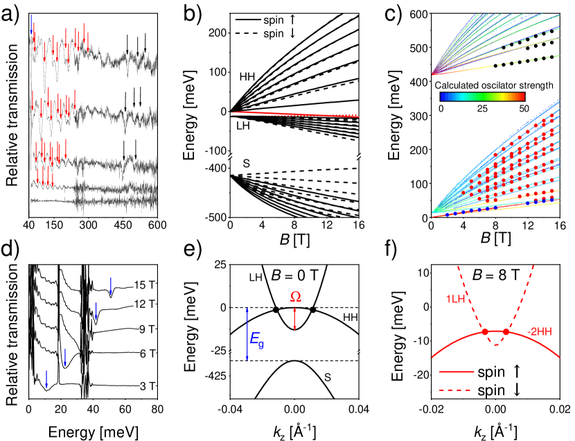
Under , the modelled bands disperse as Landau levels that are calculated and shown in Figure 3b. They are used to calculate the magneto-optical transitions that fit the absorption observed in Figure 3a. This fit is plotted in Figure 3c and shows perfect agreement with the experimental data. The two interband series are attributed to HH – LH transitions at low energy and to S – LH transitions above \qty400. The band parameters used for the fit are listed in Table 2 and the determined band structure, calculated accordingly, is plotted in Figure 3e.
The band structure of -Sn is of the same type as that of HgTe. Indeed, the gap is found to be large and negative, meaning that the S band lies under the LH and HH bands, i.e., the band structure is inverted. Therefore, properties similar to HgTe are expected, in particular, our results suggest that a quantum spin Hall phase occurs in -Sn quantum wells (see SI for additional details) [63]. The gap of -Sn is found to be relatively large as indicated by the nearly linearly-dispersive magneto-optical transitions, and more directly by the zero-field extrapolation of the second interband series (red arrows in Figure 3a). The effective mass of the HH band is given by , and that of the conduction band (LH) writes:
where is the electron rest mass and in our case. Therefore, the magneto-optical measurements result in , which is in reasonable agreement with the transport experiments performed in this work and with the literature [55, 62]. Note that the parameter , which originates from strain, accounts for a 4% correction to the effective mass. It is determined as from the extrapolation at the zero field and the shape of the first interband series (black arrows in Figure 3a). This parameter is directly related to the strain following , therefore, using the strain values measured by XRD in this work, we can deduce the shear deformation potential as , in perfect agreement with Ref. [18]. This value is very high compared to other semiconductors such as Si, HgTe or III-Vs, which display [64].
Magneto-optical experiments have demonstrated that strain is a particularly efficient tool to tune the band structure in -Sn, and a value as small as is sufficient to induce a DSM phase. Note that in our measurements, which means that the LH band goes under the HH band near the -point (see Figure 3e). Therefore, it is responsible for the emergence of two Dirac nodes located around
The distance between the two Dirac nodes is then determined as \qty0.018Å^-1 in the investigated strained -Sn epilayers with . These nodes are two-fold degenerate at and are thus Dirac in nature. When the magnetic field is applied, the two spin components are split and Dirac nodes are turned into Weyl nodes. They are formed by the remaining dispersion of the Landau level originating from the HH band, and the Landau level from the LH band. These Landau levels are highlighted in Figure 3b and their -dispersion has been calculated (see Figure 3f). Note that while the magnetic field changes the nature of the nodes from Dirac to Weyl, it also brings them closer and eventually leads to their annihilation.
| Parameter | Value |
|---|---|
Our magneto-optical experiments thus demonstrate the presence of a Dirac semimetal phase in compressively strained -Sn by accurately measuring for . Additionally, the band structure has been accurately calculated by experimentally determining the set of band structure parameters.
2.3 ARPES
The band structure, described in subsection 2.2, was directly investigated in ARPES experiments. Despite multiple reports for -Sn layers grown on InSb [28, 29, 8, 19, 30, 31, 32, 33, 34, 35], ARPES studies for samples fabricated on CdTe are still lacking. Here, we present an analysis of photoemission spectra obtained for the dedicated series of (001) -Sn/CdTe/GaAs heterostructures with varied thicknesses. The samples were transferred to the synchrotron facility without breaking ultra-high vacuum (UHV) (see section 4), before performing any characterization other than RHEED. The observed spectra turned out to be thickness-independent and their properties are summarized in Figure 4. The remaining data can be found in the SI. The observed features are consistent with the previous results, obtained for layers grown on InSb, and with the model described in subsection 2.2. Regardless of their dispersion and topological character, all of the states revealed by our ARPES studies originate only from -Sn, as can be seen from the core level spectrum in Figure 4b.
The band structure close to the point of the Brillouin zone consists of the bulk heavy hole (HH) and s-type (S) bands. The energy splitting between the S and HH bands at , eV, is consistent with our magneto-optical measurements. These bulk bands are accompanied by two types of surface states, labelled SS1 and SS2. As can be seen in Figure 4a, they have different spectral weights depending on the photon energy and can be resolved after applying the curvature procedure [65]. Both SS1 and SS2, as well as bulk HH states, are also clearly seen along direction (Figure 4c) and show anisotropy consistent with previous reports of -Sn/InSb (001) [31, 35]. To elucidate the topography of the states in more detail, we present a set of experimental constant energy contours (CECs) (Figure 4d). While SS1 is isotropic and shows a circular cross-section, the SS2 and HH states show anisotropic dispersion. We suggest that SS1, with linear Dirac-like dispersion, emerges from the band inversion and therefore has a topological origin, similar to another surface state (SS3) presented in SI and previous experimental works for strained -Sn on (001) InSb [30, 35]. The origin of SS2 has recently been attributed to the Rashba effect, originating from inversion symmetry breaking at the surface, as demonstrated by the investigation performed on -Sn/InSb (001) [35]. However, the absence of the Rashba split states with a reduced -Sn thickness to several monolayers, while observing the TI phase, raises questions. Moreover, no reliable evidence of the Rashba effect has been acquired by other means, such as magneto-transport measurement (see subsection 2.4). Consequently, alternative origins should be considered, such as the presence of Dyakonov-Khaetskii (DK) or Volkov-Pankratov (VP) states [66, 67]. The existence of such massive surface states has recently been proposed for strained Luttinger semimetals [68, 69] and the physical origin of their appearance is the hybridization of Dirac spectrum with HH states.
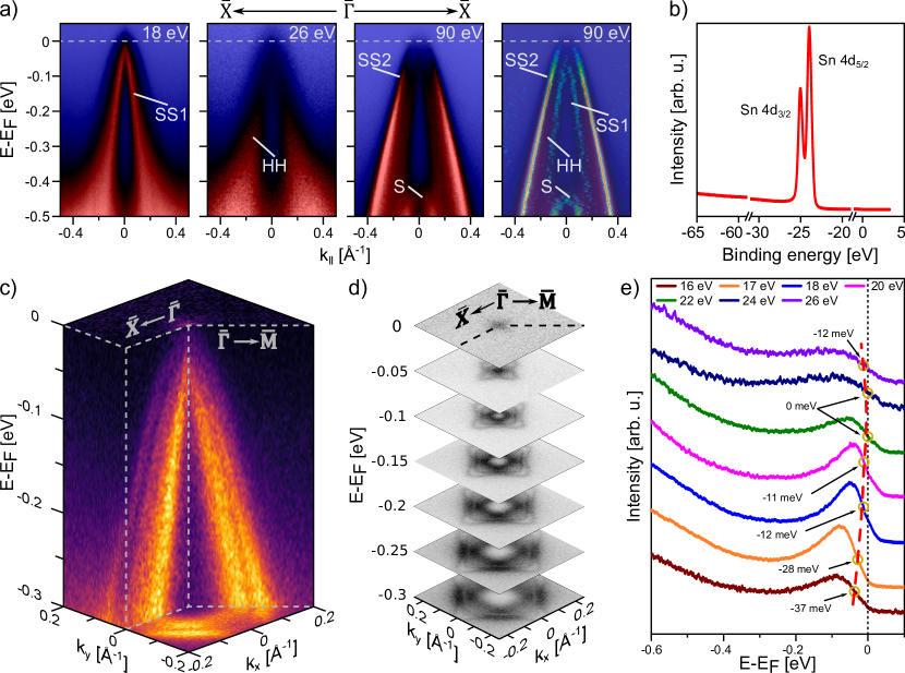
As determined in subsection 2.2, the tetragonal distortion present in the studied -Sn layers ( according to the RSM presented in Figure 2g,h) results in the presence of a DSM phase. Therefore, spectra of the bulk HH Dirac-like states are expected to change with the variation of the photon energy. In Figure 4e, the energy dispersive curve profiles extracted at normal emission of different photon energies indeed display a modest dispersion, a pattern consistent with the observation of DSM by magneto-optics. It must, however, be acknowledged that this dispersion could potentially arise from intensity suppression of SS2 due to a change in the matrix element (as detailed in the SI). Moreover, the close proximity of the two Dirac points along precludes their definitive resolution with ARPES. On the other hand, the band structure analogous to the observed structure has been reported in recent studies elucidating the DSM phase in -Sn grown on InSb (001) substrates, where akin strains of similar magnitude and sign are present [19, 31, 35]. Additionally, certain features observed in our experiment, such as point-like Fermi surface and the existence of SS1, SS2, and SS3 are theoretically predicted for the DSM phase [6, 7, 52, 30]. Thus, we believe that, in agreement with our magneto-optics measurements, considering previous experimental and theoretical works we unequivocally validated the existence of DSM in (001) -Sn/CdTe/GaAs heterostructures.
2.4 Transport properties
To get further insight into the electronic structure of -Sn, we performed magneto-transport studies of samples A - D, also examined by magneto-optics. Previous reports show that the high-temperature electronic transport of -Sn is influenced by the contribution of thermally excited carriers from the L-band [40, 70, 71, 60]. This is also true for the studied layers, as discussed in SI. Therefore, field-dependent transport studies presented here were restricted to , where only carriers from the vicinity of the -point contribute to the electronic transport due to the complete freeze-out of electrons from the L-band. Measurements were performed on samples patterned in standard Hall bars or microstructures with two perpendicular arms, presented in LABEL:fig:sample_sketch, in two distinct configurations: in addition to , examined in magneto-optics, magneto-transport was studied in the orientation with magnetic field laying in-plane (). More details on sample preparation and experimental setup can be found in the section 4.
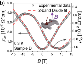
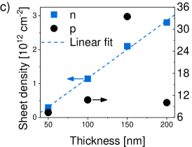
In , the longitudinal resistivity, , of all samples is positive and does not show any signs of saturation up to \qty14.5, as presented in LABEL:fig:Hall_200nm for sample D. Low-field longitudinal and Hall () resistivity can be simultaneously described by the 2-band Drude model (see LABEL:fig:Hall_200nm and SI). Fitting to the experimental data provides carrier densities and mobilities of electrons and holes for all layers. Mobility reaches for n-type carriers in sample D, confirming its high quality already observed in magneto-optical spectra. Electron densities are of the order of for all layers. The observed multicarrier behavior is in line with previous reports on -Sn grown on CdTe [40, 70, 71, 60]. However, so far no clear explanation of the source of p-type carriers has been given. We note that the electron sheet density (LABEL:fig:SheetDensity_vs_Thickness) scales linearly with the thickness of the layer, whereas no scaling is observed for holes. That leads us to the conclusion that p-type carriers originate from the (trivial) surface states observed in ARPES, while electrons are related to the bulk of -Sn. Importantly, the CdTe/GaAs substrate does not contribute to the transport properties of the studied structures, contrary to the layers fabricated on InSb [32, 36, 37, 38, 39]. Magneto-transport features in beyond the Drude model, e.g. SdH oscillations, will be described later in the text.
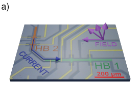
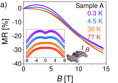
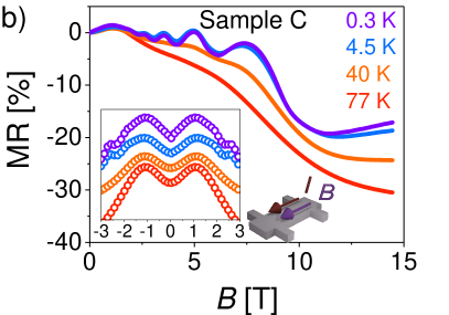
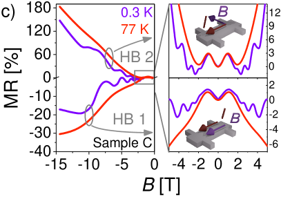
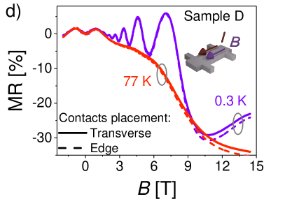
After rotating the sample from to , the character of magnetoresistance (MR) changes. Perpendicular parts of two-arm structures are no longer equivalent, with current flowing either parallel () or perpendicular () to the magnetic field (see LABEL:fig:sample_sketch). The dependence of MR on the relative orientation between current and magnetic field is summarized in Figure 6a-c for samples A and C (the qualitative behavior of samples B, C and D is the same), which represent the low- and high-mobility cases. In , MR first increases, and after reaching a maximum at , depending on the thickness, it starts to decrease with an increasing magnetic field, a behavior known as negative longitudinal magnetoresistance (NLMR). This trend persists to 14.5 T without turning back to positive MR. Strong SdH oscillations are superimposed on the low-temperature NLMR of sample C (see LABEL:fig:NLMR_150nm). Above \qty40, they are strongly damped, and the negative character of the MR is unambiguously seen. In contrast, the overall MR is positive in (LABEL:fig:NLMR_HB1HB2). The low-field MR, shown in the insets of LABEL:fig:NLMR_50nm,LABEL:fig:NLMR_150nm for the , is discussed in SI.
The NLMR was observed in some of the -Sn/InSb samples studied previously [32, 36], while other reports explicitly claim the absence of this feature [37, 39]. Its detailed analysis in the grey tin is still lacking. Our study clearly shows that it is an effect related to the material properties of -Sn and not a sample-specific feature, as it appears in all examined layers, regardless of their thickness, shape, and dimensions of the patterned microstructure or carrier density and mobility. In other compounds, such as the Weyl semimetal TaAs [72, 73] and the Dirac semimetal Na3Bi [74], NLMR was explained as a signature of a chiral anomaly. This phenomenon can be effectively described as the creation and annihilation of particles with opposite chirality and was predicted for a crystal with linearly dispersing chiral bands [45, 46, 47], such as in Weyl semimetals. Thus, it is tempting to consider the NLMR as evidence of the presence of a WSM phase. Such interpretation would agree with the results of the ARPES and magneto-optics data, as well as with previous theoretical predictions [6]. However, some concerns have been raised about other mechanisms that can result in similar behaviour [75, 76]. The list includes weak localization (WL) [77, 78], current jetting effect [79, 80], and magnetism-related phenomena [81, 82, 83]. The experimental features of NLMR in the investigated structures allow us to rule out all of these effects. Weak localization would be present in any direction of the magnetic field, which is not the case for the NLMR in the current study. As shown in LABEL:fig:NLMR_trans_cont_edge_cont, various pairs of the voltage probes yield the same result in the , which excludes the current-jetting effect [75, 84]. The presence of magnetic impurities was not only highly improbable due to the high purity of the MBE growth process but also excluded by core-level spectroscopy. Therefore, we attribute the NLMR in the grey tin to the chiral anomaly of the Weyl fermions. The description of our results in frames of semiclassical theory [46, 85], together with an analysis of alternative sources of NLMR, is presented in SI.
Finally, we move to the analysis of SdH oscillations, which are present in both and . The analysis of these oscillations proved useful in determining the band topology of multiple materials, including -Sn in both the TI [32] and DSM [36, 40] phases. To analyze SdH oscillations, we have converted resistivity to the conductivity using conductivity tensor, since fundamentally the quantization occurs in conductivity rather than in resistivity [86]. The oscillatory part of the can be described by the Lifshitz-Kosevitch equation (LK) [87, 86, 88], which in the 3D case takes the following form:
| (1) |
is the frequency of oscillations, is the Berry phase of the carriers and is a phase shift related to the dimensionality of the system and the cross-section of the Fermi surface ( for the 2D case). It is expected that in topological (normal) materials [89, 90]. and are constant; and are the damping coefficients:
| (2) |
| (3) |
Above, is a cyclotron frequency with being the cyclotron mass, and is a Dingle temperature, related to the quantum scattering time , and therefore to the quantum mobility .
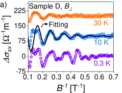
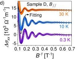
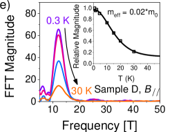
The oscillatory component of of sample D is shown as open symbols in LABEL:fig:DSIGxx_200nm_Bperp and LABEL:fig:DSIGxx_200nm_Bparal for the and , respectively. Low-temperature oscillations in exhibit multi-frequency character, confirmed by the fast Fourier transformation (FFT) spectra displayed in LABEL:fig:FFT_200nm_Bperp. Also, the Zeeman spin splitting is visible for the maximum at . Contrary to , SdH oscillations in show a single-frequency character in the full temperature range, with the FFT peak centered at \qty12 (LABEL:fig:FFT_200nm_Bparal). We conclude that the plethora of massive surface states is responsible for the multi-frequency character of the SdH oscillation in at low temperatures. By fitting Equation 2 to the temperature-dependent FFT magnitude we determined the electron cyclotron mass , as presented in the inset of LABEL:fig:FFT_200nm_Bparal. A similar value was obtained for . We have also calculated the Dingle temperatures for using Equation 3 [86], and obtained values in the range of \qtyrange[range-phrase=–, range-units=single]3040, which corresponds to the quantum mobility of \qtyrange[range-phrase=–, range-units=single]40002500^2^-1sec^-1.
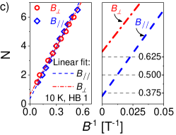
The Berry phase of the carriers is usually obtained from analysis of the Landau-level fan diagram. The minima (maxima) of are labelled with integers (half-integers) and plotted versus their position in . According to Equation 1, the intercept of the linear fit to the data yields the Berry phase. In the case of sample D, this procedure gives depending on the direction of the magnetic field, as shown in LABEL:fig:LLplot_200nm_BperpBparal. The different sign of the phase shift indicates an anisotropic Fermi surface, with a maximum cross-section at the and a minimum at the for electrons [91]. It agrees with the angle dependence of the frequency of the SdH oscillations, and the frequency increases when the field orientation is changed from the perpendicular to the parallel.
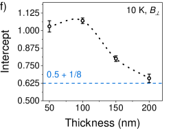
Since we determined all the parameters of the band structure that affect the LK equation, we can fit it to the experimental data with few adjustable parameters, namely the amplitude and the offset , and the Dingle temperature for . A single cosine term was used for the fitting. The results of this procedure are shown by solid lines in LABEL:fig:DSIGxx_200nm_Bperp, LABEL:fig:DSIGxx_200nm_Bparal for and , respectively. The good agreement between the fitting curves and the experimental data confirms the correct determination of the parameters. Most importantly, the oscillations in sample D show a nontrivial Berry phase, as expected for topological semimetals. However, we note that a certain thickness dependence of the phase was observed in the studied -Sn samples, as shown in LABEL:fig:LLplot_vs_thickn. Such a dependence can be caused by the hybridization between bulk Dirac electrons and massive surface states. Although the exact source of this dependence requires additional investigation, it is consistent with the previous reports, showing that in thinner layers of grey tin, the Berry phase obtained from the linear fit to the LL fan diagram deviates from the ideal value of [32, 36].
3 Conclusions
We presented the first comprehensive study of the electronic structure of compressively-strained -Sn on insulating substrates by a variety of experimental techniques. The magneto-optical results provide a set of band-structure parameters, which allow us to fully describe grown epilayers as a 3D Dirac semimetal. We found that the band structure is inverted, as expected, and determined the value by which the valence band is shifted to due strain, . The band structure is also visualized in ARPES experiments, which reveals the presence of several bulk and surface states, distinct in nature. The topological nature of the investigated samples is further proved by magneto-transport studies. After ruling out alternative possibilities, we explain the presence of negative longitudinal magnetoresistance by the chiral anomaly of the Weyl fermions. Shubnikov-de Haas oscillations reveal both the 3D nature of the Fermi surface and its non-trivial character, through observation of the Berry phase shift. We argue that the observation of these peculiar magneto-transport effects was only possible due to the insulating character of the substrates used for the growth.
We also wish to stress the practical aspect of our work. High-quality CdTe substrates of large size are currently not available. On the other hand, the growth of CdTe buffers on GaAs is well-established. It gives the possibility of wafer-scale epitaxy of -Sn if hybrid substrates are used. The high crystalline quality and homogeneous strain of the obtained layers clearly indicate that this is a promising route that may evoke progress in applied studies. It also opens new possibilities, as other buffers can be used, such as Cd1-xZnxTe or magnetically-doped CdTe, giving access to a wider range of biaxial compressive strains and to magnetism-proximatized phenomena. We also note that the fabrication of CdTe/Sn/CdTe quantum wells is a path for exploration of the QSHI state in -Sn. We, therefore, conclude that grey tin is a promising material for the exploration of various phenomena related to nontrivial topology and relativistic-like band structure, with the potential for large-scale fabrication for industrial purposes.
4 Experimental section
MBE growth Sample synthesis was carried out in two steps in two interconnected MBE Veeco GENxplor growth chambers, with a base pressure below mbar, using effusion cells with elemental Cd, Zn and Te for buffer, and Sn for -Sn, as sources. Semi-insulating epi-ready (001) GaAs from AXT, Inc. were used as substrates. First, in chamber one, several nanometer layers of ZnTe () were deposited on the GaAs substrate to alleviate the lattice constant difference between GaAs () and CdTe () and to ensure (001) growth [92], as well as to improve misfit stress relaxation of the buffer layer [93]. Then a thick CdTe buffer was grown at \qtyrange295325 to ensure a fully relaxed layer [94, 95]. The material flux ratio was controlled by a beam flux monitor placed in front of the substrate position. The growth was performed under Cd-rich conditions. After the deposition of the buffer layer, the structure was transferred to the second growth chamber, without breaking the vacuum, where -Sn deposition took place. Epitaxial growth was carried out at a temperature below \qty10 with a material flux ratio and deposition rate controlled by a quartz crystal microbalance (QCM) placed in front of the substrate position. In both cases, the structural quality of the films was monitored in-situ in real-time by reflection high-energy electron diffraction (RHEED).
Structural characterization The surface of the grown films was examined by atomic force microscopy (AFM) in tapping mode with a Bruker MultiMode 8-HR microscope. XRD patterns were recorded with the PANalytical X’Pert Pro MRD diffractometer with a 1.6 kW X-ray tube using CuK1 radiation (), a symmetric 2 Ge (220) monochromator and 2D Pixel detector. Samples for TEM observations in the form of cross-sectional lamellas were made using the FIB method. The lamellas were cut perpendicular to the sample surface in the [100] and [110]. Platinum as a protective material was deposited onto the sample surface. For TEM examinations, the Titan Cubed 80-300 transmission electron microscope operated with an acceleration voltage of 300 kV was used.
ARPES The electronic band structure of the films was examined by angle-resolved photoemission spectroscopy at URANOS (former UARPES) beamline at the SOLARIS synchrotron (Kraków, Poland) with photon energies ranging from 16 to 90 eV using horizontally polarized light at temperatures ranging from liquid nitrogen to RT. To record high-quality spectra, Scienta Omicron DA30L photoelectron spectrometer with an energy resolution of 1.8 eV and angular resolution of \qty0.1 was used. Core-level (CL) spectra were measured with a photon energy of 90 eV to determine the surface elemental composition. The experiments were carried out at pressures below mbar. The investigated -Sn epilayers were transported to the ARPES system in a battery-operated ion getter pumped Ferrovac VSN40S ultra-high vacuum (UHV) suitcase [96] sustaining a base pressure below mbar, without breaking UHV.
Magneto-optics Magneto-optical absorption experiments are performed in an Oxford Instruments 1.5 K/15 T cryostat at 4.5 K. Spectra are acquired using a Bruker Fourier transform spectrometer. All measurements are made in Faraday geometry. A globar and a Hg lamp are employed as the mid-infrared and far-infrared sources to measure the absorptions. Measurements are performed at fixed magnetic fields between 0 and 15 T. A He-cooled bolometer is used to detect the transmitted signal. The relative transmission at a fixed magnetic field, T(B)/T(B = 0), is extracted and analyzed.
Hall bars preparation The samples were patterned in the Hall bars by etching in diluted HCl, with the use of a PMMA mask defined by electron-beam lithography. The dimensions of the Hall bars are . Ti/Au contacts were deposited in the ultra-high vacuum e-beam evaporator. The samples were kept at room temperature at all stages of microfabrication. Selected layers were patterned into microstructures with two perpendicular arms. One of them was equipped with voltage probes that span across the channel (transverse contacts) in addition to standard probes at the edges of the Hall bar (edge contacts).
Magneto-transport Magneto-transport measurements were performed in a He-3 refrigerator (HelioxVL, Oxford Instruments, temperature range \qtyrange0.3100), equipped with a piezoelectric motor that allows in-situ rotation of the sample in the magnetic field. Tree distinct orientations of magnetic field were applied: , with magnetic field normal to the sample plane (i.e. standard Hall configuration), , with an in-plane magnetic field parallel to the current flow and , with in-plane magnetic field perpendicular to the current. The standard low-frequency lock-in technique, with an excitation current not exceeding , was used to collect the signal.
Acknowledgments
The authors thank T. Dietl for valuable discussions. The research was partially supported by the Foundation for Polish Science through the IRA Program co-financed by the EU within the SG OP (Grant No. MAB/2017/1) and by ANR-19-CE30-022-01 (ENS) and the Austrian Science Funds FWF (Project I-4493). This publication was partially developed under the provision of the Polish Ministry of Science and Higher Education project ”Support for research and development with the use of research infrastructure of the National Synchrotron Radiation Centre SOLARIS” under contract nr 1/SOL/2021/2. We acknowledge SOLARIS Centre for the access to the Beamline URANOS (former UARPES) where the measurements were performed.
Author contributions
J.P.: Investigation - magneto-transport & processing, Analysis, Writing - original draft; G.K.: Investigation - magneto-optics, Analysis, Writing - original draft; A.K.: Investigation - magneto-transport, Analysis, Writing – review & editing, Conceptualization, Supervision; B.T.: Investigation - MBE growth & ARPES, Analysis, Writing - original draft; J.B.O.: Investigation - magneto-optics, Analysis; R.R.: Investigation - MBE growth & ARPES; T.W.: Investigation - Processing; P.D.: Investigation - TEM; M.A.: Investigation - AFM; W.Z.: Investigation - MBE growth; B.K.: Investigation - TEM; Z.M.: Investigation - ARPES; M.R.: Investigation - ARPES; N.O.: Investigation - ARPES; L.-A.de V.: Investigation - magneto-optics, Analysis; Y.G.: Investigation - magneto-optics, Analysis; T.Wojtowicz: Supervision, Funding acquisition, Writing – review & editing; V.V.V.: Investigation - MBE growth, ARPES, XRD, Analysis, Writing – original draft, review & editing, Conceptualization, Supervision.
References
- [1] J.. Plumbridge “Tin pest issues in lead-free electronics solders” In Journal of Material Science: Materials in Electronics 18, 2007, pp. 307–318 DOI: 10.1007/s10854-006-9025-3
- [2] M. Pendharkar et al. “Parity-preserving and magnetic field-resilient superconductivity in InSb nanowires with Sn shells” In Science 372.6541, 2021, pp. 508–511 DOI: 10.1126/science.aba5211
- [3] Sabbir A. Khan et al. “Epitaxially Driven Phase Selectivity of Sn in Hybrid Quantum Nanowires” In ACS Nano 17.12, 2023, pp. 11794–11804 DOI: 10.1021/acsnano.3c02733
- [4] Malcolm J.. Jardine et al. “First-Principles Assessment of CdTe as a Tunnel Barrier at the -Sn/InSb Interface” In ACS Applied Materials & Interfaces 15.12 ACS Publications, 2023, pp. 16288–16298 DOI: 10.1021/acsami.3c07924
- [5] Liang Fu and Charles Kane “Topological insulators with inversion symmetry” In Physical Review B 76.4 American Physical Society, 2007, pp. 045302 DOI: 10.1103/PhysRevB.76.045302
- [6] Huaqing Huang and Feng Liu “Tensile strained gray tin: Dirac semimetal for observing negative magnetoresistance with Shubnikov–de Haas oscillations” In Physical Review B 95 American Physical Society, 2017, pp. 201101 DOI: 10.1103/PhysRevB.95.201101
- [7] Dongqin Zhang et al. “Engineering topological phases in the Luttinger semimetal -Sn” In Physical Review B 97 American Physical Society, 2018, pp. 195139 DOI: 10.1103/PhysRevB.97.195139
- [8] J.-C. Rojas-Sánchez et al. “Spin to Charge Conversion at Room Temperature by Spin Pumping into a New Type of Topological Insulator: -Sn Films” In Physical Review Letters 116 American Physical Society, 2016, pp. 096602 DOI: 10.1103/PhysRevLett.116.096602
- [9] Jinjun Ding et al. “Large Damping Enhancement in Dirac-Semimetal–Ferromagnetic-Metal Layered Structures Caused by Topological Surface States” In Advanced Functional Materials 31.11, 2021, pp. 2008411 DOI: https://doi.org/10.1002/adfm.202008411
- [10] Jinjun Ding et al. “Switching of a Magnet by Spin-Orbit Torque from a Topological Dirac Semimetal” In Advanced Materials 33.23, 2021, pp. 2005909 DOI: https://doi.org/10.1002/adma.202005909
- [11] Federico Binda et al. “Spin-orbit torques and magnetotransport properties of -Sn and -Sn heterostructures” In Physical Review B 103 American Physical Society, 2021, pp. 224428 DOI: 10.1103/PhysRevB.103.224428
- [12] Yansong Zhu et al. “Microsized Gray Tin as a High-Rate and Long-Life Anode Material for Advanced Sodium-Ion Batteries” In Nano Letters 22.19 ACS Publications, 2022, pp. 7976–7983 DOI: 10.1021/acs.nanolett.2c03334
- [13] An-Qi Wang, Xing-Guo Ye, Da-Peng Yu and Zhi-Min Liao “Topological Semimetal Nanostructures: From Properties to Topotronics” PMID: 32286783 In ACS Nano 14.4, 2020, pp. 3755–3778 DOI: 10.1021/acsnano.9b07990
- [14] Matthew J Gilbert “Topological electronics” In Communications Physics 4.1 Nature Publishing Group UK London, 2021, pp. 70 DOI: 10.1038/s42005-021-00569-5
- [15] Keita Ishihara et al. “Giant superconducting diode effect in ion-beam patterned Sn-based superconductor nanowire/topological Dirac semimetal planar heterostructures” In arXiv preprint arXiv:2308.00893, 2023
- [16] Steven Groves and William Paul “Band Structure of Gray Tin” In Physical Review Letters 11 American Physical Society, 1963, pp. 194–196 DOI: 10.1103/PhysRevLett.11.194
- [17] Fred H. Pollak et al. “Energy-Band Structure and Optical Spectrum of Grey Tin” In Physical Review B 2 American Physical Society, 1970, pp. 352–363 DOI: 10.1103/PhysRevB.2.352
- [18] B.. Roman and A.. Ewald “Stress-Induced Band Gap and Related Phenomena in Gray Tin” In Physical Review B 5 American Physical Society, 1972, pp. 3914–3932 DOI: 10.1103/PhysRevB.5.3914
- [19] Cai-Zhi Xu et al. “Elemental Topological Dirac Semimetal: -Sn on InSb(111)” In Physical Review Letters 118 American Physical Society, 2017, pp. 146402 DOI: 10.1103/PhysRevLett.118.146402
- [20] G.. Coster, P.. Folkes, P.. Taylor and O.. Vail “Effects of orientation and strain on the topological characteristics of CdTe/-Sn quantum wells” In Physical Review B 98 American Physical Society, 2018, pp. 115153 DOI: 10.1103/PhysRevB.98.115153
- [21] Yong Xu et al. “Large-Gap Quantum Spin Hall Insulators in Tin Films” In Physical Review Letters 111 American Physical Society, 2013, pp. 136804 DOI: 10.1103/PhysRevLett.111.136804
- [22] Menghan Liao et al. “Superconductivity in few-layer stanene” In Nature Physics 14.4 Nature Publishing Group UK London, 2018, pp. 344–348 DOI: 10.1038/s41567-017-0031-6
- [23] Joseph Falson et al. “Type-II Ising pairing in few-layer stanene” In Science 367.6485, 2020, pp. 1454–1457 DOI: 10.1126/science.aax3873
- [24] Sumanta Kumar Sahoo and Kung-Hwa Wei “A Perspective on Recent Advances in 2D Stanene Nanosheets” In Advanced Materials Interfaces 6.18, pp. 1900752 DOI: https://doi.org/10.1002/admi.201900752
- [25] Wlodek Zawadzki “Semirelativity in semiconductors: a review” In Journal of Physics: Condensed Matter 29.37, 2017, pp. 373004 DOI: 10.1088/1361-648X/aa7932
- [26] David Hillman, Ross Wilcoxon and Amy Wieland “An Examination of the Tin Pest Phenomenon Over a 10-Years Period” In Journal of Electronic Materials 51 Springer, 2022, pp. 6492–6502 DOI: https://doi.org/10.1007/s11664-022-09886-z
- [27] R… Farrow et al. “The growth of metastable, heteroepitaxial films of -Sn by metal beam epitaxy” In Journal of Crystal Growth 54.3, 1981, pp. 507–518 DOI: https://doi.org/10.1016/0022-0248(81)90506-6
- [28] A. Barfuss et al. “Elemental Topological Insulator with Tunable Fermi Level: Strained -Sn on InSb(001)” In Physical Review Letters 111 American Physical Society, 2013, pp. 157205 DOI: 10.1103/PhysRevLett.111.157205
- [29] Yoshiyuki Ohtsubo, Patrick Le Fèvre, Fran Bertran and Amina Taleb-Ibrahimi “Dirac Cone with Helical Spin Polarization in Ultrathin -Sn(001) Films” In Physycal Review Letters 111 American Physical Society, 2013, pp. 216401 DOI: 10.1103/PhysRevLett.111.216401
- [30] Victor A. Rogalev et al. “Double band inversion in -Sn: Appearance of topological surface states and the role of orbital composition” In Physical Review B 95 American Physical Society, 2017, pp. 161117 DOI: 10.1103/PhysRevB.95.161117
- [31] M.. Scholz et al. “Topological surface state of -Sn on InSb(001) as studied by photoemission” In Physical Reviev B 97 American Physical Society, 2018, pp. 075101 DOI: 10.1103/PhysRevB.97.075101
- [32] Quentin Barbedienne et al. “Angular-resolved photoemission electron spectroscopy and transport studies of the elemental topological insulator -Sn” In Physical Review B 98 American Physical Society, 2018, pp. 195445 DOI: 10.1103/PhysRevB.98.195445
- [33] V.. Rogalev et al. “Tailoring the topological surface state in ultrathin -Sn(111) films” In Physical Review B 100 American Physical Society, 2019, pp. 245144 DOI: 10.1103/PhysRevB.100.245144
- [34] Ivan Madarevic et al. “Structural and electronic properties of the pure and stable elemental 3D topological Dirac semimetal -Sn” In Applied Physics Letters Materials 8.3, 2020, pp. 031114 DOI: 10.1063/1.5142841
- [35] K… Chen et al. “Thickness-dependent topological phase transition and Rashba-like preformed topological surface states of -Sn(001) thin films on InSb(001)” In Physical Review B 105 American Physical Society, 2022, pp. 075109 DOI: 10.1103/PhysRevB.105.075109
- [36] Le Duc Anh et al. “Elemental Topological Dirac Semimetal -Sn with High Quantum Mobility” In Advanced Materials 33.51, 2021, pp. 2104645 DOI: https://doi.org/10.1002/adma.202104645
- [37] Yuanfeng Ding et al. “Wafer-Scale and Topologically Nontrivial -Sn Films Grown on InSb(001) by Molecular-Beam Epitaxy” In Physical Reviev Applied 17 American Physical Society, 2022, pp. 014015 DOI: 10.1103/PhysRevApplied.17.014015
- [38] Ivan Madarevic et al. “Easily Accessible Topologically Protected Charge Carriers in Pure and Robust -Sn Films” In physica status solidi (RRL) – Rapid Research Letters n/a.n/a, 2022, pp. 2200161 DOI: https://doi.org/10.1002/pssr.202200161
- [39] Yuanfeng Ding et al. “Transport evidence of the spin-polarized topological surface states of -Sn grown on CdTe by molecular beam epitaxy” In Applied Physics Letters 121.9, 2022, pp. 093102 DOI: 10.1063/5.0098585
- [40] Owen Vail et al. “Growth and Magnetotransport in Thin-Film -Sn on CdTe” In physica status solidi (b) 257.1, 2020, pp. 1800513 DOI: https://doi.org/10.1002/pssb.201800513
- [41] Yuanfeng Ding et al. “Multiple carrier transport in high-quality -Sn films grown on CdTe (001) by molecular beam epitaxy” In Journal of Vacuum Science & Technology A 39.3, 2021, pp. 033408 DOI: 10.1116/6.0000756
- [42] R.. Bicknell et al. “Growth of (100)CdTe films of high structural perfection on (100)GaAs substrates by molecular beam epitaxy” In Applied Physics Letters 44.3, 1984, pp. 313–315 DOI: 10.1063/1.94736
- [43] G. Karczewski et al. “High mobility 2D electron gas in iodine modulation doped CdTe/CdMgTe heterostructures” In Journal of Crystal Growth 184-185, 1998, pp. 814–817 DOI: https://doi.org/10.1016/S0022-0248(98)80169-3
- [44] Karolina Wichrowska et al. “High-Resolution X-Ray Diffraction Studies on MBE-Grown p-ZnTe/n-CdTe Heterojunctions for Solar Cell Applications” In Acta Physica Polonica A 126.5 Polska Akademia Nauk. Instytut Fizyki PAN, 2014, pp. 1083–1086 DOI: 10.12693/APhysPolA.126.1083
- [45] H.B. Nielsen and Masao Ninomiya “The Adler-Bell-Jackiw anomaly and Weyl fermions in a crystal” In Physics Letters B 130.6, 1983, pp. 389–396 DOI: https://doi.org/10.1016/0370-2693(83)91529-0
- [46] D.. Son and B.. Spivak “Chiral anomaly and classical negative magnetoresistance of Weyl metals” In Physical Review B 88 American Physical Society, 2013, pp. 104412 DOI: 10.1103/PhysRevB.88.104412
- [47] A.. Burkov “Chiral Anomaly and Diffusive Magnetotransport in Weyl Metals” In Physical Review Letters 113 American Physical Society, 2014, pp. 247203 DOI: 10.1103/PhysRevLett.113.247203
- [48] D.. Price, J.. Rowe and R.. Nicklow “Lattice Dynamics of Grey Tin and Indium Antimonide” In Physical Review B 3 American Physical Society, 1971, pp. 1268–1279 DOI: 10.1103/PhysRevB.3.1268
- [49] Huanhuan Song et al. “Thermal Stability Enhancement in Epitaxial Alpha Tin Films by Strain Engineering” In Advanced Engineering Materials 21.10, 2019, pp. 1900410 DOI: https://doi.org/10.1002/adem.201900410
- [50] M.. Asom, A.. Kortan, L.. Kimerling and R.. Farrow “Structure and stability of metastable -Sn” In Applied Physics Letters 55.14, 1989, pp. 1439–1441 DOI: 10.1063/1.101580
- [51] J. Thewlis and A.R. Davey “Thermal expansion of grey tin” In Nature 174.4439 Nature Publishing Group UK London, 1954, pp. 1011–1011 DOI: 10.1038/1741011a0
- [52] Rigo A. Carrasco et al. “The direct bandgap of gray -tin investigated by infrared ellipsometry” In Applied Physics Letters 113.23, 2018, pp. 232104 DOI: 10.1063/1.5053884
- [53] Paweł T. Jochym et al. “Influence of anharmonicity on the negative thermal expansion of -Sn” In Phys. Rev. Mater. 6 American Physical Society, 2022, pp. 113601 DOI: 10.1103/PhysRevMaterials.6.113601
- [54] Werner Martienssen “Semiconductors. Gallium comppounds” In Springer Handbook of Condensed Matter and Materials Data Springer, 2005, pp. 621–685
- [55] S.. Groves, C.. Pidgeon, A.. Ewald and R.. Wagner “Interband magnetoreflection of -Sn” In Journal of Physics and Chemistry of Solids 31.9, 1970, pp. 2031–2049 DOI: https://doi.org/10.1016/0022-3697(70)90006-5
- [56] C.. Pidgeon and R.. Brown “Interband Magneto-Absorption and Faraday Rotation in InSb” In Physical Review 146 American Physical Society, 1966, pp. 575–583 DOI: 10.1103/PhysRev.146.575
- [57] G.. Bir and G.. Pikus “Symmetry and strain-induced effects in semiconductors” John WileySons, 1974
- [58] Lucien D. Laude, Fred H. Pollak and Manuel Cardona “Effects of Uniaxial Stress on the Indirect Exciton Spectrum of Silicon” In Physical Review B 3 American Physical Society, 1971, pp. 2623–2636 DOI: 10.1103/PhysRevB.3.2623
- [59] J.. Luttinger “Quantum Theory of Cyclotron Resonance in Semiconductors: General Theory” In Physical Review 102 American Physical Society, 1956, pp. 1030–1041 DOI: 10.1103/PhysRev.102.1030
- [60] C.. Hoffman et al. “Three-band transport and cyclotron resonance in -Sn and -Sn1-xGex grown by molecular-beam epitaxy” In Physical Review B 40 American Physical Society, 1989, pp. 11693–11700 DOI: 10.1103/PhysRevB.40.11693
- [61] T. Wojtowicz et al. “Far-infrared determination of cyclotron and plasma-shifted cyclotron resonances in thin MBE-grown films of -Sn” In Semiconductor Science and Technology 5.3S, 1990, pp. S248 DOI: 10.1088/0268-1242/5/3S/054
- [62] W.. Yuen, W.. Liu, R.. Stradling and B.A. Joyce “The growth and electronic properties of -Sn thin films grown on InSb(100) and (111) substrates by molecular beam epitaxy (MBE)” In Journal of Crystal Growth 111.1, 1991, pp. 943–947 DOI: https://doi.org/10.1016/0022-0248(91)91112-N
- [63] Sebastian Küfner, Lars Matthes and Friedhelm Bechstedt “Quantum spin Hall effect in -Sn/CdTe(001) quantum-well structures” In Physical Review B 93 American Physical Society, 2016, pp. 045304 DOI: 10.1103/PhysRevB.93.045304
- [64] Fred H. Pollak “Chapter 2: Effects of Homogeneous Strain on the Electronic and Vibrational Levels in Semiconductors” In Strained-Layer Superlattices: Physics 32, Semiconductors and Semimetals Elsevier, 1990, pp. 17–53 DOI: https://doi.org/10.1016/S0080-8784(08)62642-3
- [65] P. Zhang et al. “A precise method for visualizing dispersive features in image plots” In Review of Scientific Instruments 82.4, 2011, pp. 043712 DOI: 10.1063/1.3585113
- [66] M.. D’yakonov and A.. Khaetskiǐ “Surface states in a gapless semiconductor” In Soviet Journal of Experimental and Theoretical Physics Letters 33, 1981, pp. 110 URL: http://jetpletters.ru/ps/1501/article_22948.pdf
- [67] O.. Pankratov, S.. Pakhomov and B.. Volkov “Supersymmetry in heterojunctions: Band-inverting contact on the basis of Pb1-xSnxTe and Hg1-xCdxTe” In Solid State Communications 61.2, 1987, pp. 93–96 DOI: https://doi.org/10.1016/0038-1098(87)90934-3
- [68] Alexander Khaetskii, Vitaly Golovach and Arnold Kiefer “Revisiting the physical origin and nature of surface states in inverted-band semiconductors” In Physical Review B 105 American Physical Society, 2022, pp. 035305 DOI: 10.1103/PhysRevB.105.035305
- [69] Maxim Kharitonov, Julian-Benedikt Mayer and Ewelina M. Hankiewicz “Evolution of the surface states of the Luttinger semimetal under strain and inversion-symmetry breaking: Dirac, line-node, and Weyl semimetals”, 2022 arXiv:2212.00902 [cond-mat.mes-hall]
- [70] Charles F. Lavine and A.. Ewald “Two-band galvanomagnetic effects in gray tin” In Journal of Physics and Chemistry of Solids 32.6, 1971, pp. 1121–1140 DOI: https://doi.org/10.1016/S0022-3697(71)80170-1
- [71] Li‐Wei Tu, George K. Wong and John B. Ketterson “Observation of quantum size effect in the resistivity of thin, gray tin epilayers” In Applied Physics Letters 55.13, 1989, pp. 1327–1329 DOI: 10.1063/1.101645
- [72] Xiaochun Huang et al. “Observation of the Chiral-Anomaly-Induced Negative Magnetoresistance in 3D Weyl Semimetal TaAs” In Phys. Rev. X 5 American Physical Society, 2015, pp. 031023 DOI: 10.1103/PhysRevX.5.031023
- [73] Cheng-Long Zhang et al. “Signatures of the Adler-Bell-Jackiw chiral anomaly in a Weyl fermion semimetal” In Nature Communications 7, 2016, pp. 10735 DOI: 10.1038/ncomms10735
- [74] Jun Xiong et al. “Evidence for the chiral anomaly in the Dirac semimetal Na3Bi” In Science 350.6259, 2015, pp. 413–416 DOI: 10.1126/science.aac6089
- [75] R.. Reis et al. “On the search for the chiral anomaly in Weyl semimetals: the negative longitudinal magnetoresistance” In New Journal of Physics 18.8 IOP Publishing, 2016, pp. 085006 DOI: 10.1088/1367-2630/18/8/085006
- [76] Yupeng Li et al. “Negative magnetoresistance in Weyl semimetals NbAs and NbP: Intrinsic chiral anomaly and extrinsic effects” In Frontiers of Physics 12.3, 2017, pp. 127205 DOI: 10.1007/s11467-016-0636-8
- [77] Arisato Kawabata “Theory of Negative Magnetoresistance I. Application to Heavily Doped Semiconductors” In Journal of the Physical Society of Japan 49.2, 1980, pp. 628–637 DOI: 10.1143/JPSJ.49.628
- [78] A. Kawabata “Theory of negative magnetoresistance in three-dimensional systems” In Solid State Communications 34.6, 1980, pp. 431–432 DOI: https://doi.org/10.1016/0038-1098(80)90644-4
- [79] A.. Pippard “Magnetoresistance in metals” New York: Cambridge University Press, 2009
- [80] Jingshi Hu, T.. Rosenbaum and J.. Betts “Current Jets, Disorder, and Linear Magnetoresistance in the Silver Chalcogenides” In Phys. Rev. Lett. 95 American Physical Society, 2005, pp. 186603 DOI: 10.1103/PhysRevLett.95.186603
- [81] H. Ohno et al. “Magnetotransport properties of p-type (In,Mn)As diluted magnetic III-V semiconductors” In Phys. Rev. Lett. 68 American Physical Society, 1992, pp. 2664–2667 DOI: 10.1103/PhysRevLett.68.2664
- [82] S… Parkin “Giant Magnetoresistance in Magnetic Nanostructures” In Annual Review of Materials Science 25.1, 1995, pp. 357–388 DOI: 10.1146/annurev.ms.25.080195.002041
- [83] A.. Ramirez “Colossal magnetoresistance” In Journal of Physics: Condensed Matter 9.39, 1997, pp. 8171 DOI: 10.1088/0953-8984/9/39/005
- [84] Sihang Liang et al. “Experimental Tests of the Chiral Anomaly Magnetoresistance in the Dirac-Weyl Semimetals Na3Bi and GdPtBi” In Physical Review X 8 American Physical Society, 2018, pp. 031002 DOI: 10.1103/PhysRevX.8.031002
- [85] Jennifer Cano et al. “Chiral anomaly factory: Creating Weyl fermions with a magnetic field” In Physical Review B 95 American Physical Society, 2017, pp. 161306 DOI: 10.1103/PhysRevB.95.161306
- [86] Yoichi Ando “Topological Insulator Materials” In Journal of the Physical Society of Japan 82.10, 2013, pp. 102001 DOI: 10.7566/JPSJ.82.102001
- [87] D Schoenberg “Magnetic oscillations in metals” New York: Cambridge University Press, 1984
- [88] H. Murakawa et al. “Detection of Berry’s Phase in a Bulk Rashba Semiconductor” In Science 342.6165, 2013, pp. 1490–1493 DOI: 10.1126/science.1242247
- [89] G.. Mikitik and Yu.. Sharlai “Manifestation of Berry’s Phase in Metal Physics” In Physical Review Letters 82 American Physical Society, 1999, pp. 2147–2150 DOI: 10.1103/PhysRevLett.82.2147
- [90] G.. Mikitik and Yu.. Sharlai “Berry phase and the phase of the Shubnikov–de Haas oscillations in three-dimensional topological insulators” In Physical Review B 85 American Physical Society, 2012, pp. 033301 DOI: 10.1103/PhysRevB.85.033301
- [91] Hai-Peng Sun and Hai-Zhou Lu “Quantum transport in topological semimetals under magnetic fields (II)” In Frontiers of Physics 14, 2019, pp. 33405 DOI: 10.1007/s11467-019-0890-7
- [92] H. Shtrikman, M. Oron, A. Raizman and G. Cinader “Determining the [001] crystal orientation of CdTe layers grown on (001) GaAs” In Journal of Electronic Materials 17, 1988, pp. 105–110 DOI: 10.1007/BF02652138
- [93] H. Nishino, I. Sugiyama and Y. Nishijima “Misfit stress relaxation mechanism in CdTe(100) and CdTe/ZnTe(100) on a GaAs(100) highly mismatched heteroepitaxial layer” In Journal of Applied Physics 80.6, 1996, pp. 3238–3243 DOI: 10.1063/1.363265
- [94] H. Tatsuoka, H. Kuwabara, Y. Nakanishi and H. Fujiyasu “Strain relaxation of CdTe(100) layers grown by hot‐wall epitaxy on GaAs(100) substrates” In Journal of Applied Physics 67.11, 1990, pp. 6860–6864 DOI: 10.1063/1.346079
- [95] A Khiar et al. “In-well pumped mid-infrared PbTe/CdTe quantum well vertical external cavity surface emitting lasers” In Applied Physics Letters 104.23 AIP Publishing, 2014 DOI: 10.1063/1.4882081
- [96] Bartłomiej Turowski et al. “Spin-polarization of topological crystalline and normal insulator Pb1-xSnxSe (111) epilayers probed by photoelectron spectroscopy” In Applied Surface Science 610, 2023, pp. 155434 DOI: https://doi.org/10.1016/j.apsusc.2022.155434