Tuning the flat bands by the interlayer interaction, spin-orbital coupling and electric field in twisted homotrilayer MoS2
Abstract
Ultraflat bands have already been detected in twisted bilayer graphene (TBG) and twisted bilayer transition metal dichalcogenides (tb-TMDs), which provide a platform to investigate strong correlations. In this paper, the electronic properties of twisted trilayer molybdenum disulfide (TTM) are investigated via an accurate tight-banding Hamiltonian. We find that the highest valence bands are derived from -point of the constituent monolayer, exhibiting a graphene-like dispersion or becoming isolated flat bands. The lattice relaxation, local deformation, and electric field can significantly tune the electronic structures of TTM with different starting stacking arrangements. After introduce the spin-orbital coupling (SOC) effect, we find a spin-valley-layer locking effect at the minimum of conduction band at K- and K′-point of the Brillouin zone, which may provide a platform to study optical properties and magnetoelectric effects.
I Introduction
Since the discovery of the single-layer graphene, research on two-dimensional (2D) materials has drawn significant attention in the scientific community [1]. Stacking 2D materials with the rotation angle or lattice mismatch between layers, moiré superlattices with periodicity that ranges from nanometers to micrometers can be formed [2, 3, 4]. Rotation angle and lattice mismatch , as degrees of freedom, could tune the electronic structures of the moiré systems. In twisted bilayer graphene (TBG), when the rotation angle approaches 1.05∘, the so-called magic angle, two van Hove singularities (VHS) in the density of states (DOS) merge in the charge neutrality point, resulting in a sharp peak associated with flat bands [5, 2]. In such flat band system, exotic phenomena, including unconventional superconductivity [6, 7], strong correlations [8], quantum anomalous Hall effect [9], ferromagnetism [10] and electronic collective excitations [5, 11] have been observed, which are not observed in the parent material.
Flat bands are also detected in many other moiré systems, for example, twisted hexagonal boron nitride [12], twisted bilayer transition metal dichalcogenides (tb-TMDs) [13, 14]. In fact, both the structural and electronic structures of tb-TMDs are remarkably different from that of TBG: Firstly, the appearance of flat bands are different. Flat bands are observed in tb-TMDs with twist angles below 7∘ [15, 16, 17, 18, 19, 20, 21, 22, 14], but only special angles in TBG [2]. Secondly, the localization of the flat band states in real space are different. In TBG, the flat band states at the K-point of the Brillouin zone (BZ) are concentrated in the AA region [23]. The tb-TMDs have two distinct configurations and the localization of the flat band states at the -point of the BZ are different [13, 24]. Thirdly, the lattice relaxation changes differently the distribution of stackings and interlayer spacings in the two different configurations. Finally, tb-TMDs is a new model system to explore quantum phenomena, for example, moiré excitons [25, 26], Wigner crystal [20], pair density waves [27] and plasmons [28].
Multilayer graphene moiré systems also possess flat bands, for example, twisted trilayer systems and even twisted multilayer superlattices [29]. Different from the twisted bilayer, twisted multilayer systems are more flexible and controllable, which can be easily tuned by twist angles, starting stacking arrangements and external fields [30]. Furthermore, the moiré of moiré twisted trilayer graphene (TTG) has extended magic phase [4, 31], and electric field-tunable superconductivity was observed in mirror-symmetry TTG [32, 33]. Recently, several groups have started to explore the electronic structures of twisted multilayer TMDs. For example, twisted trilayer with two different twist angles is successfully fabricated in experiment, which reveals multiple moiré exciton splitting peaks due to the presence of deeper moiré potential [34]. The ABBA-stacked twisted double bilayer WSe2 could be served as a realistic and tunable platform to simulate -valley honeycomb lattice with both sublattice and SU(2) spin rotation symmetries [35]. The ABAB-stacked double bilayer WSe2 as a platform to study electronic correlations within the -valley moiré bands, could have a control over the spin and valley character of the correlated ground and excited states via the electromagnetic fields [36]. However, the detailed knowledge of the electronic structures of twisted multilayer transition metal dichalcogenides is still missing.
In this paper, we use a tight-binding model to study the electronic properties of twisted trilayer molybdenum disulfide (TTM) with different starting stacking arrangements. Similar to TTG, the electronic structures of TTM depends strongly on the starting stacking arrangements. By modulating the arrangement, isolated flat bands could be achieved in the valence band edge. Previous investigations show that lattice relaxation has a significant impact on the electronic properties of TBG and tb-TMDs [37, 28, 38]. We find that the lattice relaxation has distinct influence on electronic properties of TTM with different configurations. Furthermore, these configurations response differently to the external electric field. By manuplating these degree of freedoms, for instance, the arrangements, the strain, spin-orbital coupling (SOC) and the electric field, we could tune the flat bands in TTM, creating a promising platform for exploring the strongly correlated states. The paper is organized as follows: In Sec. II, we introduce the TTM structure and the numerical methods. In Sec. III, we investigate the flat bands in TTM with different starting stacking arrangements, and tune the flat bands with the interlayer interaction, spin-orbital coupling and external electric fields. Finally, we give a summary in Sec. IV.
II Methods
In TBG, the AA and AB starting stacking arrangements give exactly the same band structures, whereas the electronic structures in twisted trilayer graphene are strongly dependent on the starting stacking arrangements [30, 39]. In the bilayer TMDs, unlike graphene, the inversion symmetry is present in AB (2H) stacking but broken in AA (3R) stacking. The AB twisted TMDs have AB regions form a honeycomb network, and the AA twisted one has the AA regions form a triangular lattice. Consequently, these two distinct moiré systems show different electronic properties [13, 38, 14]. That is, the bandwidth and localization of the flat bands are significantly different in these two distinct tb-TMDs. The starting stacking arrangements may also play a significant role in the twisted trilayer MoS2.
II.1 The atomic structures
In this paper, we focus on two different starting stacking arrangements AAB and AAA. Based on these two trilayer stackings, we rotate the middle layer to construct a commensurate TTM. Note that only one moiré pattern is formed here, which is different from the moiré-of-moiré pattern [4]. Similar to the bilayer structures, the basis vectors in the TTM can be expressed as
| (1) |
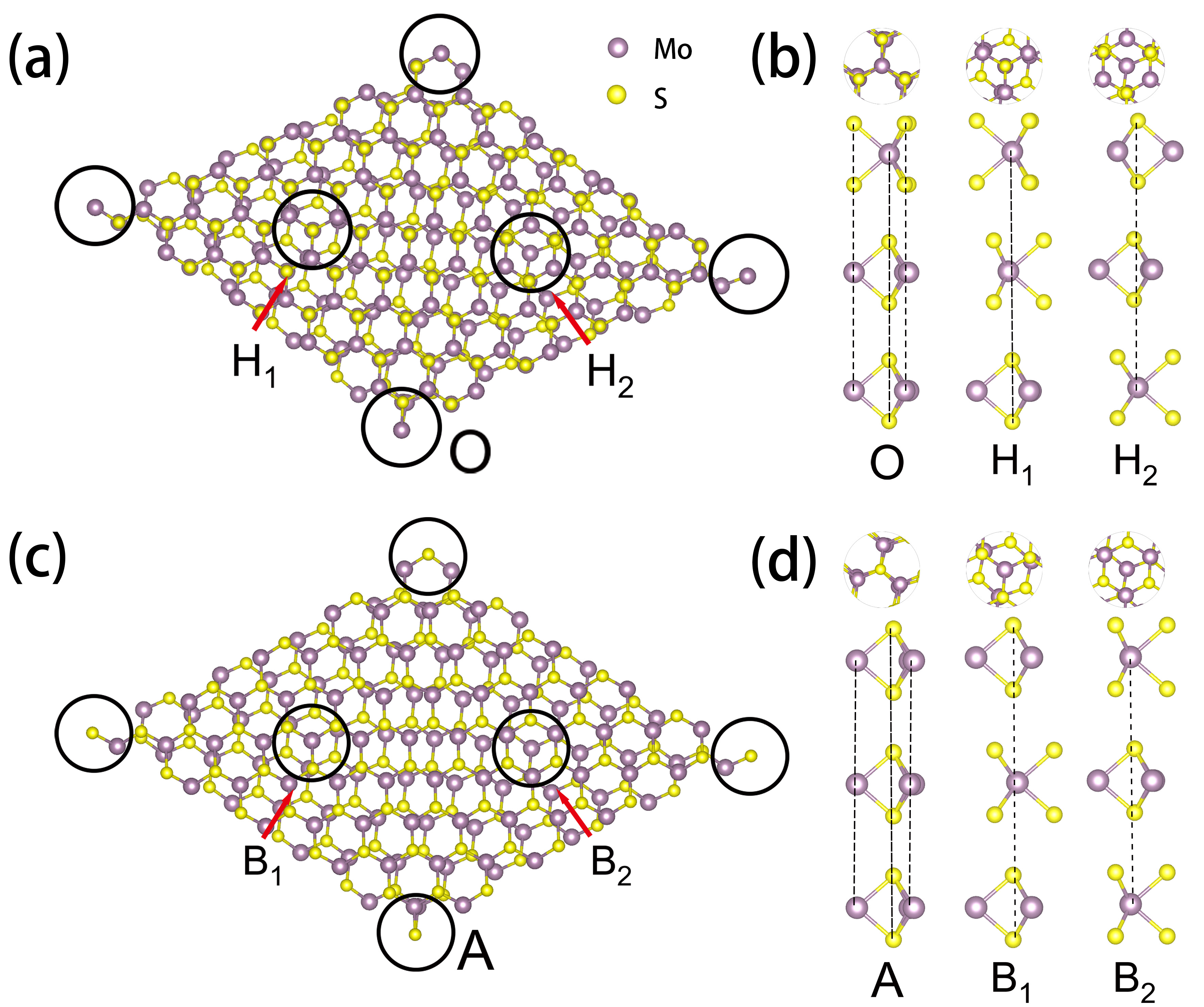
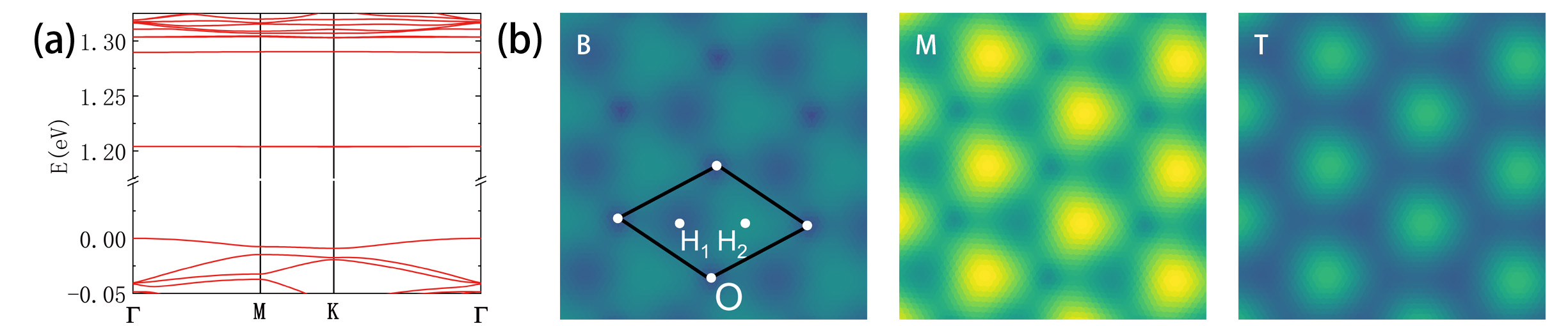
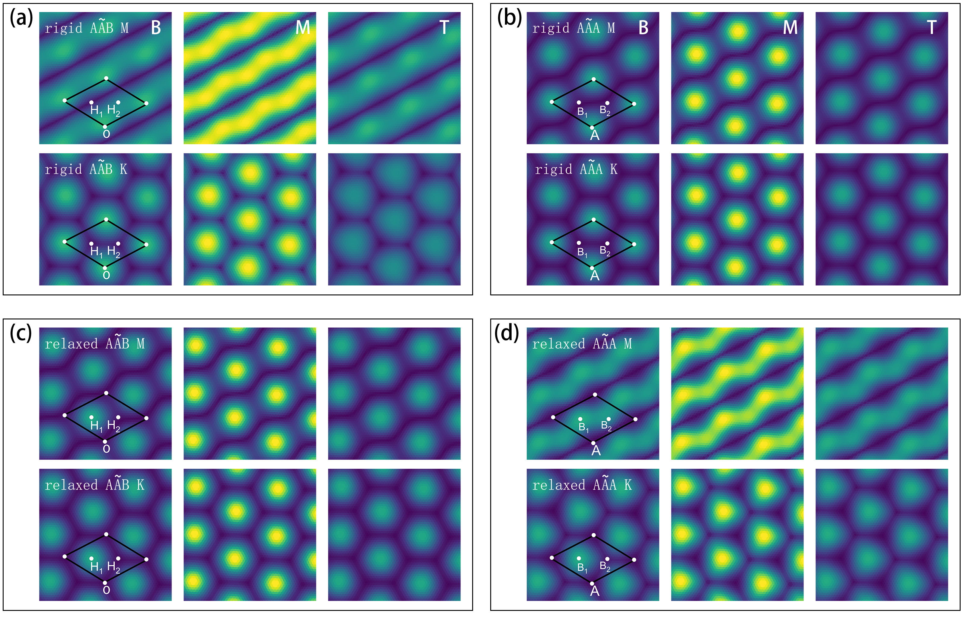
where , are the vectors of monolayer with nm being the lattice constant, and and are positive prime integers with which means that the moiré supercell contains only one moiré pattern. Another two parameters to determine the structure of are the vertical distance between sulfur atoms within monolayer nm and the vertical distance between the layers nm. The twist angle is , and the number of atoms in each moiré supercell is . In our calculation, the integer pair gives a twist angle , and one unit cell contains 993 atoms and 1986 atoms. We use the notations - and - stand for these two configurations. The number 3.15 represents the twist angle, and the twisted middle layer is marked by a tilde above the letter. Figure 1 shows the atomic structure of and , in which the atoms inside the parallelogram form a unit cell. There are three different types of high-symmetry points in each unit cell, that is, the O, H1 and H2 high-symmetry stackings in the , shown in Fig. 1(b) and the A, B1 and B2 high-symmetry stackings in the , shown in Fig. 1(d).
II.2 Tight-binding model
We employ a tight-binding model to calculate the electronic properties of TTM [38, 40]. The Hamiltonian of the TB model can be expressed as
| (2) |
where are the Hamiltonian of monolayer , and are the interlayer interactions of bottom-middle layers and middle-top layers, respectively. The primitive cell of monolayer consists of one Mo atom and two S atoms, and the relevant atomic orbital basis includes five orbitals of each Mo atom and three orbitals of each S atom. In the monolayer Hamiltonian, we only consider the interaction terms between orbitals of the same type at first neighbor positions, terms between orbitals of different types at first and second neighbor positions. Details of the TB model refer to [40, 38]. The interlayer Hamiltonian includes only the interaction between the adjacent chalcogen atoms at the interface of each bilayer, which is
| (3) |
where is the orbital basis of the th monolayer. The Slater-Koster interlayer hopping term is[40]
| (4) |
where , , , are the components of the relative position vector of orbitals and , respectively, , in which can be and , and , and are fitting parameters [40]. Some other TB models consider a interlayer coupling beyond the first-neighbor hopping [18, 24]. Note that the main conclusion in this paper will not change if we include also Mo- S and Mo- Mo interlayer hopping terms in Eq. (2) [38].
II.3 Lattice relaxation
Previous results show that the lattice reconstruction plays a significant role in the electronic structures of twisted TMDs [17, 41]. To determine the equilibrium structure of a TTM, we perform a lattice relaxation using the LAMMPS software package [42, 43]. The potentials we used in relaxation are the interlayer Lennard-Jones (LJ) potential [44] and intralayer Stilliner-Weber (SW) potential [45]. During the relaxation process, we use periodic boundary conditions in all three dimensions, leading to both in-plane and out-of-plane displacements. After the relaxation, the interlayer hopping terms are modified via Eq. (4) and intralayer hopping terms are modified with the following formula [46]
| (5) |
where is the previous intralayer hopping term between the orbital of atom and the orbital of atom, and is the corresponding new hopping term after relaxation, and are relative positions of atoms before and after relaxation, respectively, , , for S- S, S- Mo, Mo- Mo hybridizations, respectively [46].
II.4 Electronic properties
After constructing the Hamiltonian Eq. (2) of the TTM, we diagonalize the matrix to obtain the band structure and eigenstates, and adopt the tight-binding propagation method to get other electronic structures [47]. The DOS can be calculated by [48, 47]
| (6) |
where is the random initial state and S is the number of random samples. To guarantee the convergence of DOS, we calculate the DOS of a large system with more than ten millions of orbitals.
III Results and discussion
III.1 The interlayer interaction effect
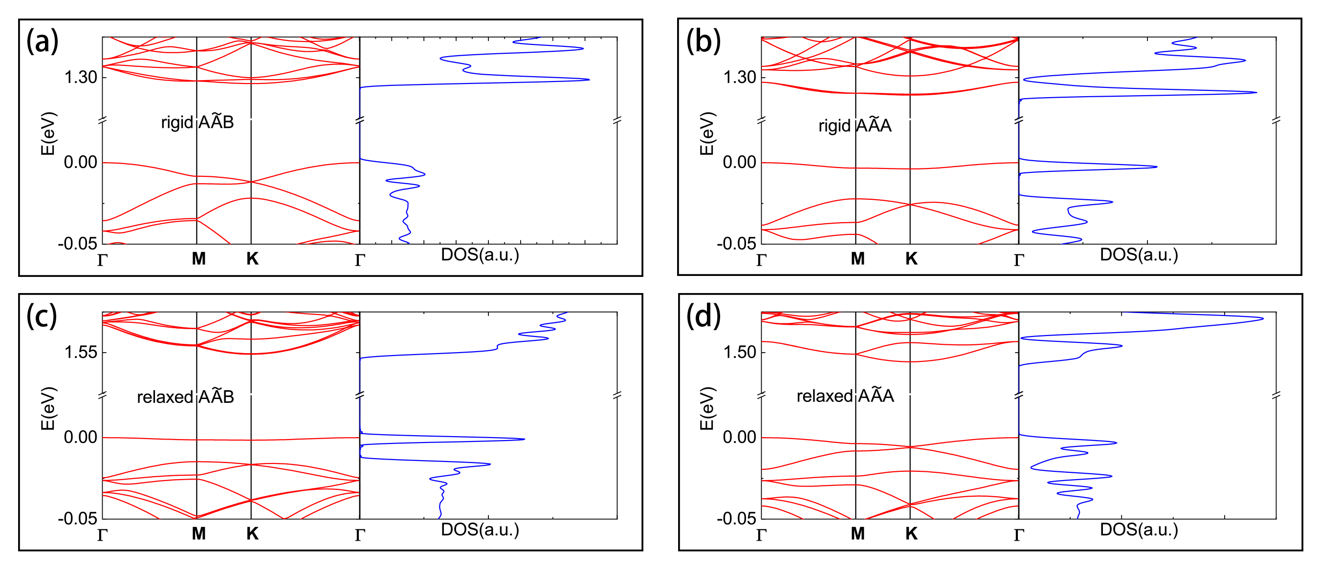
The electronic structures of the tb-TMDs have been systematically investigated [13, 38, 24, 49]. In tb-TMDs with a AA arrangement, the high-symmetry stackings include AA regions and two types of Bernal-like regions which are and . In the rigid AA case, the first (VB1) and the second (VB2) highest valence bands (VBs) are separated by a gap at the K-point of BZ. In large rotation angles, for instance , the energy of the M-point is larger than that of the K-point in the VB1 [49]. Consequently, we refer this gap as with the value defined as the energy difference between the VB1 at the K-point and VB2 at the M-point. The state of the VB1 at the -point is localized in the AA region. When the lattice relaxation is taken into account, the VB1 and VB2 touch at the K-point and the states of the VB1 at the -point localize in the and regions. The situation of the tb-TMDs with a AB arrangement is completely different. In the tb-TMDs with a AB structure, the high-symmetry stackings are AB, and . In both rigid and relaxed cases, there is a gap , with the states at the -point in the and AB regions, respectively. Moreover, in both AA and AB cases, the moiré systems exhibit a semiconducting band structure with a band gap separating the valence and conduction bands. We define this gap as , which is the energy difference between the -point of the VB1 and the K-point of the conduction band edge. Note that we focus on the valence band structure of the twisted trilayer TMDs. For simplicity, we will not include the SOC in the calculations unless we discuss about the SOC effect.
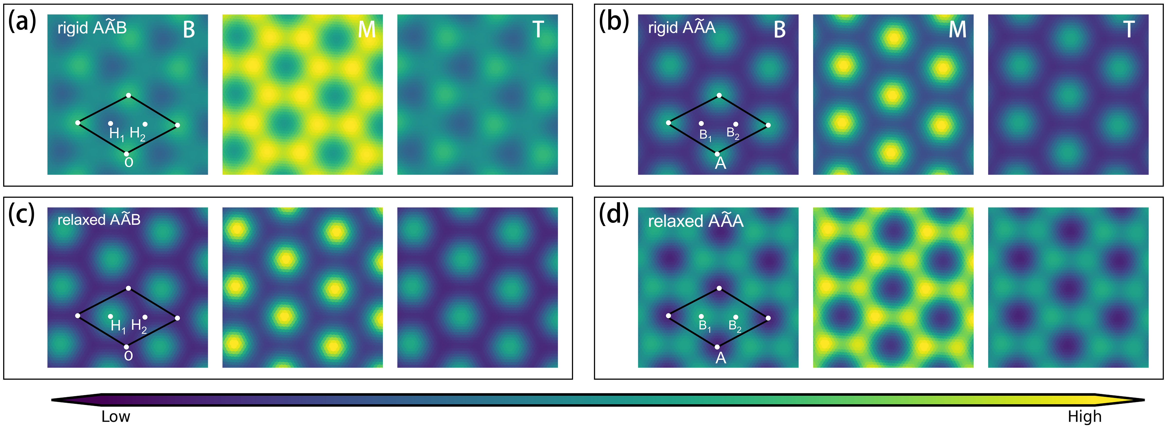
As for the homotrilayer systems, the is a combination of AA and AB moiré patterns, and the is a combination of two AA moiré patterns, which are justified by the electronic structures in Figs. 2(a), (b) and Figs. 3(a), (b). In the , the VB1 and VB2 touch at the K-point, with the states at the -point localized in both O (corresponds to the AA bilayer case) and H2 (corresponds to the AB bilayer case) regions. In the , similar to the AA bilayer case, the VB1 is isolated from other VBs, and the states at the -point of the VB1 are in the A region (illustrated in Fig. 1(d)) with a AAA stacking. The AAB arrangement could be constructed by a lateral shift of the AAA arrangement along the armchair direction. Therefore, the lateral shift is an efficient tuning node in the TTM, for instance, opening a gap between the VB1 and VB2, engineering the localization and the width of the flat bands.
The interlayer interaction could be modified by a lateral shift. Another natural way is the lattice relaxation. The out-of-plane displacements of the moiré patterns lead to local variations in the interlayer spacing (ILS) between two layers in different high-symmetry regions, resulting in the variation of the interlayer interaction. In the tb-TMDs, the lattice relaxation has a significantly effect on the flat bands [13, 38, 24]. Next, we study how will the lattice relaxation modify the flat band properties of TTM. Our findings reveal that in the relaxed , the VB1 becomes an isolated flat band, and states are localized in the H1 with S-Mo-Mo stacking. Contrarily, in the relaxed structure, the VB1 and VB2 touch at the K-point, forming a Dirac-like bands. The states of the flat band at the -point are mainly distributed in the B1 and B2 two high-symmetry points. Therefore, in the band structures plotted in the Fig. 2, there are two different types of flat bands. One is the isolated flat bands, of which the states are mainly localized in one symmetry-stacking point; the other flat band touches with VB2 at the K-point, forming a Dirac-like dispersion and states at different k points have different localization (see Appendix A). Moreover, we find that the presence or absence of the gap do not change if different potentials [50] are used in the lattice relaxation process.
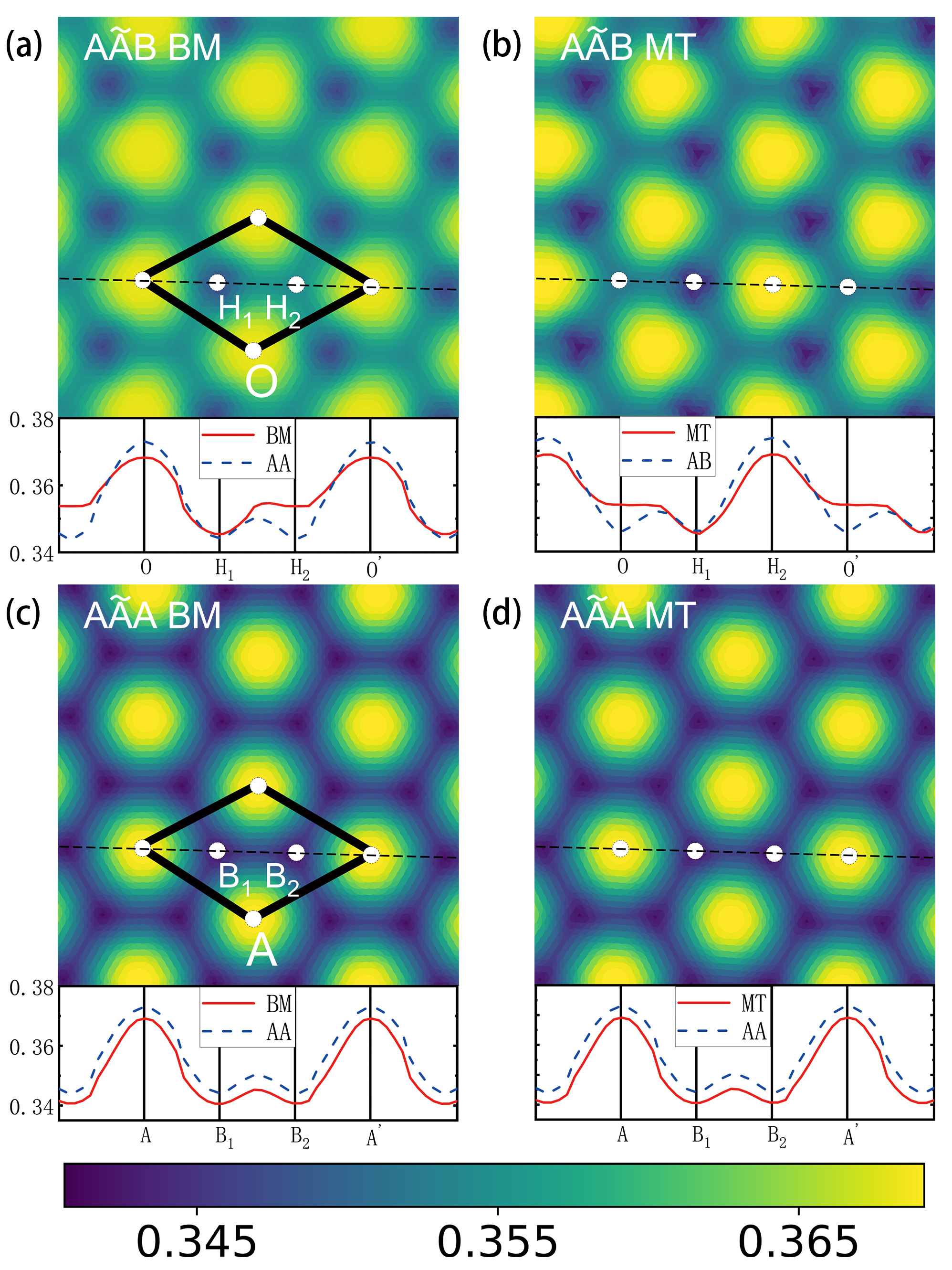
To better understand the formation of the flat bands, we analyze the ILS of the moiré systems, which are shown in Fig. 4. For comparison, we also plot the ILS of the tb-TMDs with AA and AB configurations (dashed lines). In the relaxed , the maximum ILS between the bottom layer and middle layer is at O with AA stacking, while the maximum ILS between the middle layer and top layer is at H2 with S-S stacking. Due to the presence of the third layer, the ILS of the H2 and O regions are different from that of the bilayer cases. Especially, the H2 and O in the Fig. 4(a) and (b) have larger ILS, respectively. On the contrary, the third layer has no effect to the ILS in the H1 regions. The homotrilayer AAA exhits similar relaxation patterns as homobilayer AA. There is only a global reduce of the ILS in the whole moiré pattern.
The change in electron distribution arises from the changes of the interlayer interaction in different high-symmetry stacking regions. It will be conformed by the strain effect in the following part. In the rigid form of , the strongest interlayer interaction between the bottom and middle layers occurs in the O point with AA stacking, and the strongest interlayer interaction between the middle and top layers occurs in the H2 point with S-S stacking. Different from the AAA stacking in rigid , there are two dominant stacking forms in rigid . As a result, the electron distribution of the bottom layer is concentrated in the O point, the electron distribution of the top layer is concentrated in the H2 point, and the electron distribution of the middle layer is present at both O and H2 points, as depicted in Fig. 3(a). Hence, the electrons do not exhibit localization in the TTM plane, and VB1 represents a non-isolated band in the band structure of rigid in Fig. 2(a). After relaxation, electrons are redistributed to the H1 point, where interlayer interactions are relatively stronger, resulting in the localization of VB1 in relaxed in Fig. 2(c). Similarly, for the structure, in its rigid form, the strongest interlayer interaction between the bottom and middle layers, as well as between the middle and top layers, occurs in the O point. Consequently, electrons in all three MoS2 layers are localized in the O point, and VB1 of rigid represents an isolated band in Fig. 2(b). After relaxation, the interlayer interaction in the O point weakens, and electrons are redistributed to the H1 and H2 points, causing a transition in VB1 from an isolated to a non-isolated band in Fig. 2(d).
III.2 The strain effect
We use a Gaussian bubble to modify the interlayer separation in the high-symmetry stacking of TTM, increasing the interlayer orbital distance of the AA stacking in the O point or the S-S stacking in the H2 point, respectively. The Gaussian function is in the form of , where represents the amplitude of the bubble, denotes the center of the Gauss bubble, and and are the widths of the bubble in the x and y directions. The center of the Gaussian function is at either O or H2 (calculated separately for the two cases). For example, when the center is at O, all orbitals on the bottom layer inside the bubble have their z-coordinates subtracted by , causing a movement away from the middle layer and top layer, while the middle and top layers remain unchanged. For the hopping terms, we still calculate them as we do during relaxation, with interlayer hopping terms calculated according to Slater-Koster formula in Eq. (4) and intralayer hopping corrected using Eq. (5).
We analyze the electronic properties of rigid with the modified interlayer separation. At the high-symmetry stacking points O and H2 in rigid , the stacking forms are AAB and Mo-S-S, respectively. By increasing the interlayer separation and weakening the interlayer interaction between orbitals in AA stackings at O or S-S stacking at H2, we calculate the energy bands and eigenstates of , shown in Fig. 5. The corresponding band structure and eigenstates for weakened interlayer interaction in S-S stacking are not shown here as they exhibit similar behavior to Fig. 5. When the interlayer interaction in AA stacking are weakened, electrons become localized at H2. Conversely, and when the interlayer interaction in S-S stacking are weakened, electrons are localized at O. Both of these operations cause electrons to exhibit localization in the TTM plane, and the VB1 of becomes an isolated energy band. This calculation supports our hypothesis that electrons primarily distribute at high-symmetry points with strong interlayer interactions. If there is only one high-symmetry point with dominant interlayer interaction, VB1 will be an isolated band, otherwise, if multiple high-symmetry points contribute, VB1 will touch with VB2 at the K-point.
III.3 The spin-orbital coupling effect
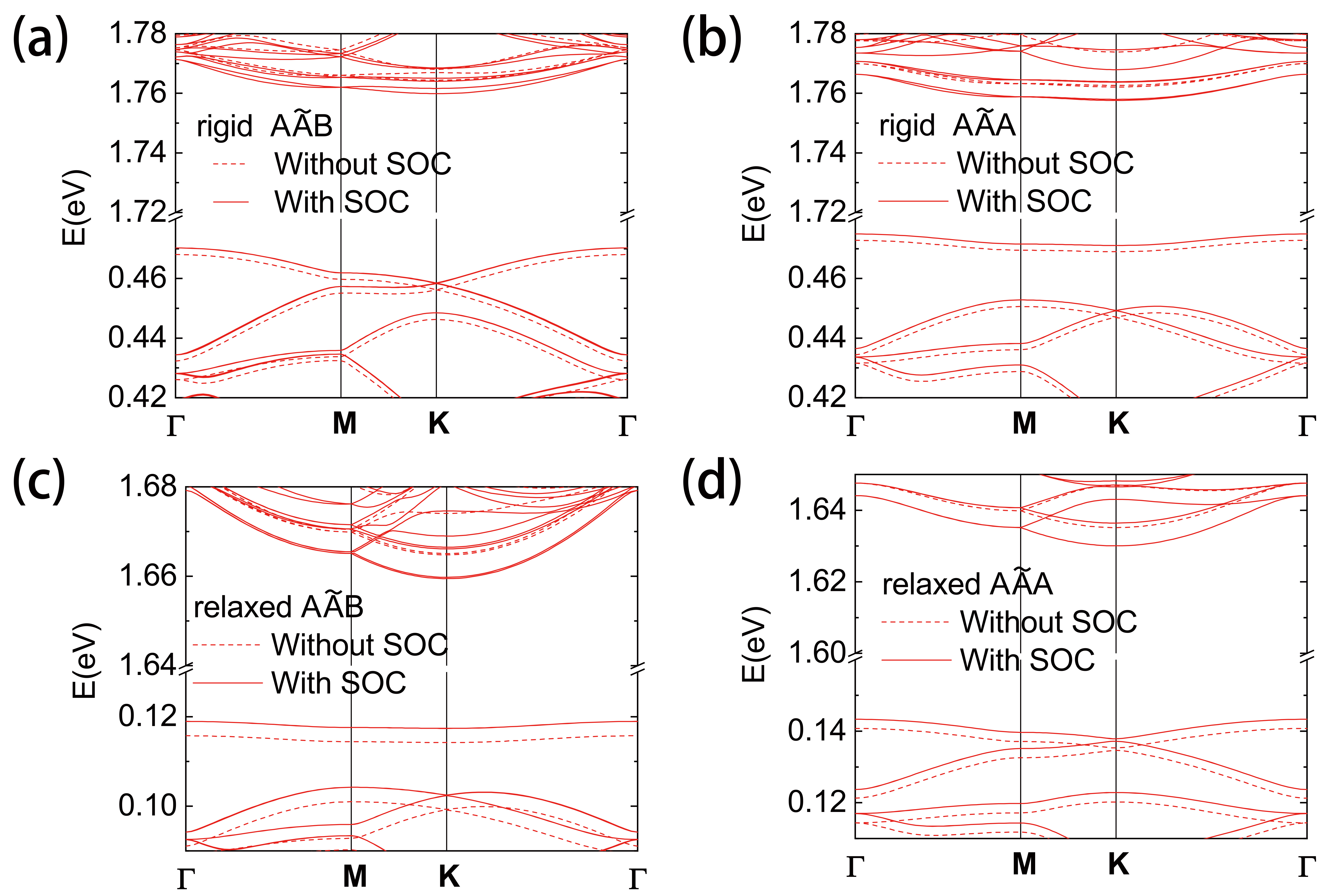
In this section, we investigate the influence of SOC effect on the band structures of TTM. We introduce the SOC in the TB Hamiltonian by doubling the orbitals and adding an atomic on-site term [40, 38, 51]. In Fig. 6, we show the band structures of and with (solid red line) and without SOC (dashed red line). It is evident that regardless of whether the structure is rigid or relaxed, the valence band edge does not split due to SOC which means the band at the valence band edge is doubly spin degenerate in the BZ. This finding is contrary to that of monolayer MoS2 and consistent with tb-TMDs [40, 38]. In contrast, there is a large splitting of the energy band at the K-point of the conduction band edge, and at the -point and M-point with time reversal symmetry, the energy bands remain spin degenerate. Moreover, the SOC decreases the gap in all cases due to the splitting of conduction band.
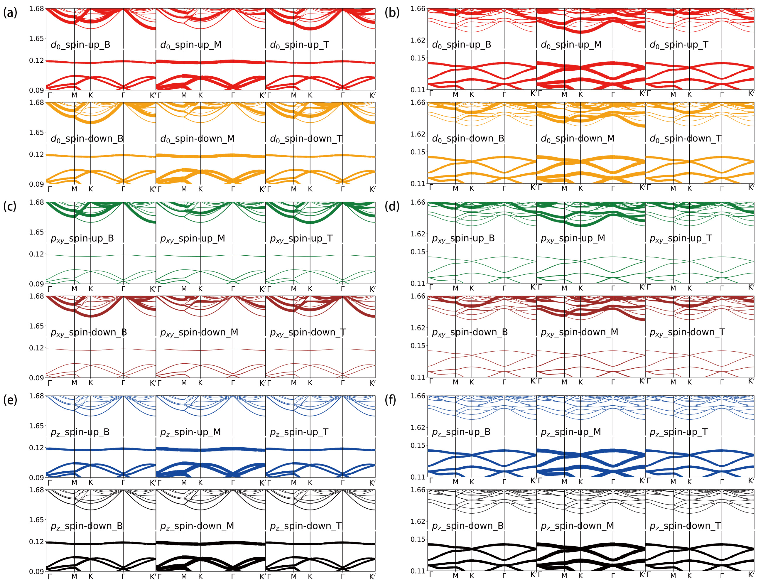
To understand the SOC effect on the flat bands, we analyze their orbital weights. Figure 7 presents the orbital weights of relaxed and relaxed . We use the thickness of the lines to represent the size of the weight, and draw separately the weight diagrams for spin-up and spin-down, as well as the orbital weights of the three layers. We can see that the d and pz orbitals play a major role in the formation of the ultraflat bands at the valence band edge, and the contribution of d and pz orbitals in the middle layer is greater than that in the bottom and top layers. This is consistent with the results in Fig. 3, which indicates that the electron distribution in the middle layer is the result of the combined action of the interlayer interaction between the bottom and middle layers. In monlayer TMD, the valence band edge at the K-point has mainly orbital character, whereas at the -point has mainly and orbital characters [52]. This suggests that the flat band in originate from the -states of the constituent monolayer. All these behaviors of the flat band at the valence band edge are also detected in the case.
The bottom of the conduction band mainly consist of and orbitals, and from Figs. 7(a) and 7(c), it’s found that at the bottom of the conduction band of relaxed , the spin-up state at the K-valley is degenerate with the spin-down state at K′-valley, and vice versa, indicating that the spin are locked to a certain valley, which is a spin-valley locking effect [38, 53]. Spin-valley locking also occurs in the electronic structure of relaxed shown in Figs. 7(b) and 7(d). The spin-valley locking effects in relaxed and relaxed are similar to the case of tb-MoS2 [38].
The three-layer MoS2 orbitals have a great difference in the contribution to the conduction band edge. The bottom layer or top layer contribute the most to the bottom of the conduction band in relaxed , while the middle layer contribute the most in relaxed , which means that the electrons in K- or K′-valley are localized in one layer of TTM. This is because the interlayer hopping is suppressed due to the spin-valley locking [54, 55, 56]. The influence of interlayer interaction on the electron distribution is greatly reduced, and electrons are localized in a certain layer, depending on the spin-valley state and layer index.
In relaxed the spin-up states in bottom layer and spin-down states in top layer are degenerate, and vice versa, indicating that there is a spin-layer locking in relaxed . This is because in the structure, the middle layer is twisted, and the bottom and top layers form a bilayer structure with 2H phase, which has inversion symmetry in real space. The inversion symmetry brings the spin-layer locking, which is similar to the results of the electronic band structure of bilayer TMDs [53, 54, 57, 58, 56]. Most of electrons in relaxed are locked in a certain layer and valley, which is the so called spin-valley-layer locking [58, 59], and the spin-layer-valley locking can be described by the coupling between electron real spin, valley pseudospin and layer pseudospin. The Hamiltonian near the K- and K′-point can be written as [54, 59, 60], in which is the SOC splitting amplitude, is the index of the K- and K′-valley pseudospin, is the index of spin up and down, is the interlayer hopping amplitude, and are the Pauli matrices for the layer pseudospin. We set the of layer A to -1, the of layer B to 1, and the of the twisted middle layer A to a value between 0 and 1 related to the twist angle. In the band structure of relaxed , the energy band at the bottom of the conduction band splits into two energy bands at K- and K′-valley due to the SOC effect. For the energy band with larger values, is satisfied, while for the energy band with smaller values, is satisfied. Thus, a spin in a valley is locked to a certain layer, indicating a spin-valley-layer locking in the bottom layer and top layer of relaxed . Meanwhile, in the band structure of relaxed , there is also two splitting bands at the bottom of conduction band. For the energy band with larger values, is satisfied, while for the energy band with smaller values, is satisfied, and , which means there is a spin-valley locking in relaxed , and there is no spin-layer locking because of the lack of inversion symmetry in . The spin-valley-layer locking effect makes a promising platform for studying optical and magnetoelectric effects involving the degrees of freedom including the real electron spin, the layer pseudospin, and the valley pseudospin [61, 55, 60, 54, 57, 56].
III.4 The electric field effect
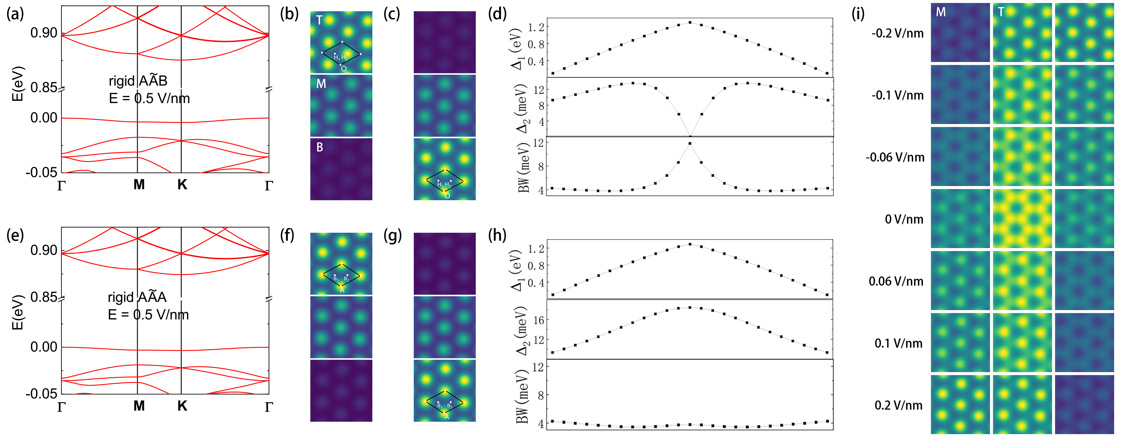
In this section, we study the response of electronic properties of TTM to the electric field. We define the electric field as positive when its direction is from the bottom to the top of TTM, and negative when it is from the top to the bottom. The effect of the electric field is considered by adding an electric potential on the onsite term in Eq. (2). As shown in Figs. 8(a) and (e), the VB1 of rigid and rigid become an isolated band when the electric field is 0.5 V/nm or -0.5 V/nm (the band structure for an electric field of -0.5 V/nm is not shown here). For rigid , when the electric field is -0.5 V/nm, the electrons are localized at H2, and when the electric field is 0.5 V/nm, the electrons are localized at O, as shown in Figs. 8 (b) and 8 (c). In contrast, Figs. 8 (e) and 8 (f) show that regardless of whether the electric field is -0.5 V/nm or 0.5 V/nm, the electrons are localized at A.
We change the electric field and calculate the gap and defined in Sec. III.1, as well as the bandwidth of VB1 (BW) as depicted in Figs. 8 (d) and 8 (h). Our results reveal that the of both rigid and rigid decrease linearly as the electric field increases, and this tendency occurs regardless of whether the electric field is positive or negative. With the electric field large enough, there will be a transition between the semiconductor and metal. Such giant Stark effect is similar to the case of tb-TMDs [62, 63]. We can find that the of rigid increases first and then decreases as the electric field increases, and reaches its maximum value around 0.5 V/nm, while BW has the opposite trend to , reaching its minimum value around 0.5 V/nm. In addition, the of rigid gradually decreases as the electric field increases, while the BW of rigid changes very little. Furthermore, we observe that , and BW are all symmetrical about E=0. In the rigid , the electric field attempts to close the gap between the VB1 and VB2. In order to understand the nonlinear changes of the with the electric field in the case, we calculate the flat band states in real space, shown in Fig. 8(i). There is a charge transfer between the three layers. A positive electric field deplete the top layer, and the system behaves like a tb-TMDs with AA arrangement. That is why the flat band states localize in the O region. Under a negative electric field, the system behaves like a tb-TMDs with AB arrangement, where the flat band states localize in the H2 region. The critical electric field is around 0.5 V/nm.
IV Conclusion
In this study, we evaluated the electronic properties of and both with and without relaxation. Our results indicate that the electronic properties of rigid are distinct from those of . Before relaxation, the VB1 of rigid intersects with VB2 at the K-point, and becomes isolated after relaxation, while has isolated and non-isolated VB1 before and after relaxation, respectively. The VB1 originates from the -states of the monolayer. We analyzed the electron distributions of the two structures and found that an isolated VB1 is usually associated with the localization of electrons at high-symmetry points, which have the strongest interlayer interactions. Rigid have only one dominant high-symmetry stacking form in their interlayer interactions, leading to the localization of electrons and an isolated VB1. However, in rigid , there are two high-symmetry stackings, AA and S-S, with strong interlayer interactions, and electrons are primarily distributed at these two regions, leading to a non-isolated VB1. We used this relationship between the interlayer interactions at high-symmetry points and electronic properties to open the gap between VB1 and VB2 in rigid by weakening the interlayer interaction of either the AA or S-S stacking. Due to the different symmetry, after introduce the SOC, we find a spin-valley-layer locking in the , whereas a spin-valley locking in the . Finally, we apply an electric field to open the gap in rigid . The gap between VB1 and VB2 is opened through the synergistic effect of interlayer interactions and the electric field. Moreover, we found that the trend of the gap of changes differently from that of with the variation of the electric field E. In the , due to the electric field, it decouples to a AA or AB tb-TMDs, opening a gap between VB1 and VB2 and changing the localization of the flat band states.
V Acknowledgements
We thank Francisco Guinea, Pierre A. Pantaleón, Adrian Ceferino and Xueheng Kuang for their useful discussions. This work was supported by the National Natural Science Foundation of China (Grant No. 12174291) and the Knowledge Innovation Program of Wuhan Science and Technology Bureau (Grant No. 2022013301015171). Z.Z. acknowledges support funding from the European Union’s Horizon 2020 research and innovation programme under the Marie Skłodowska-Curie grant agreement No. 101034431 and from the “Severo Ochoa” Programme for Centres of Excellence in R&D (CEX2020-001039-S / AEI / 10.13039/501100011033). Numerical calculations presented in this paper have been performed on the supercomputing system in the Supercomputing Center of Wuhan University.
Appendix A The eigenstates of the flat bands in and with and without relaxation
References
- Novoselov et al. [2004] K. S. Novoselov, A. K. Geim, S. V. Morozov, D. Jiang, Y. Zhang, S. V. Dubonos, I. V. Grigorieva, and A. A. Firsov, Science 306, 666 (2004).
- Bistritzer and MacDonald [2011] R. Bistritzer and A. H. MacDonald, Proc. Natl. Acad. Sci. 108, 12233 (2011).
- Geim and Grigorieva [2013] A. K. Geim and I. V. Grigorieva, Nature 499, 419 (2013).
- Foo et al. [2023] D. C. W. Foo, Z. Zhan, M. M. A. Ezzi, L. Peng, S. Adam, and F. Guinea, arXiv preprint arXiv:2305.18080 (2023).
- Kuang et al. [2021] X. Kuang, Z. Zhan, and S. Yuan, Phys. Rev. B 103, 115431 (2021).
- Sharma et al. [2020] G. Sharma, M. Trushin, O. P. Sushkov, G. Vignale, and S. Adam, Phys. Rev. Res. 2, 022040 (2020).
- Cao et al. [2018a] Y. Cao, V. Fatemi, S. Fang, K. Watanabe, T. Taniguchi, E. Kaxiras, and P. Jarillo-Herrero, Nature 556, 43 (2018a).
- Cao et al. [2018b] Y. Cao, V. Fatemi, A. Demir, S. Fang, S. L. Tomarken, J. Y. Luo, J. D. Sanchez-Yamagishi, K. Watanabe, T. Taniguchi, E. Kaxiras, R. C. Ashoori, and P. Jarillo-Herrero, Nature 556, 80 (2018b).
- Serlin et al. [2020] M. Serlin, C. L. Tschirhart, H. Polshyn, Y. Zhang, J. Zhu, K. Watanabe, T. Taniguchi, L. Balents, and A. F. Young, Science 367, 900 (2020).
- Sharpe et al. [2019] A. L. Sharpe, E. J. Fox, A. W. Barnard, J. Finney, K. Watanabe, T. Taniguchi, M. A. Kastner, and D. Goldhaber-Gordon, Science 365, 605 (2019).
- Hesp et al. [2021] N. C. Hesp, I. Torre, D. Rodan-Legrain, P. Novelli, Y. Cao, S. Carr, S. Fang, P. Stepanov, D. Barcons-Ruiz, and H. H. S. et al., Nat. Phys. 17, 1162 (2021).
- Walet and Guinea [2021] N. R. Walet and F. Guinea, Phys. Rev. B 103, 125427 (2021).
- Naik and Jain [2018] M. H. Naik and M. Jain, Phys. Rev. Lett. 121, 266401 (2018).
- Zhang et al. [2020a] Z. Zhang, Y. Wang, K. Watanabe, T. Taniguchi, K. Ueno, E. Tutuc, and B. J. LeRoy, Nat. Phys. 16, 1093 (2020a).
- Wu et al. [2018] F. Wu, T. Lovorn, E. Tutuc, and A. H. MacDonald, Phys. Rev. Lett. 121, 026402 (2018).
- Wu et al. [2019] F. Wu, T. Lovorn, E. Tutuc, I. Martin, and A. H. MacDonald, Phys. Rev. Lett. 122, 086402 (2019).
- Naik et al. [2020] M. H. Naik, S. Kundu, I. Maity, and M. Jain, Phys. Rev. B 102, 075413 (2020).
- Venkateswarlu et al. [2020a] S. Venkateswarlu, A. Honecker, and G. Trambly de Laissardière, Phys. Rev. B 102, 081103 (2020a).
- Jin et al. [2019] C. Jin, E. C. Regan, A. Yan, M. I. B. Utama, D. Wang, S. Zhao, Y. Qin, S. Yang, Z. Zheng, and S. S. et al, Nature 567, 76 (2019).
- Regan et al. [2020] E. C. Regan, D. Wang, C. Jin, M. I. B. Utama, B. Gao, X. Wei, S. Zhao, W. Zhao, Z. Zhang, and K. Y. et al., Nature 579, 359 (2020).
- Tang et al. [2020] Y. Tang, L. Li, T. Li, Y. Xu, S. Liu, K. Barmak, K. Watanabe, T. Taniguchi, A. H. MacDonald, J. Shan, and K. F. Mak, Nature 579, 353 (2020).
- Wang et al. [2020] L. Wang, E.-M. Shih, A. Ghiotto, L. Xian, D. A. Rhodes, C. Tan, M. Claassen, D. M. Kennes, Y. Bai, and B. K. et al., Nat. Mater. 19, 861 (2020).
- Guinea and Walet [2018] F. Guinea and N. R. Walet, Proc. Natl. Acad. Sci. 115, 13174 (2018).
- Vitale et al. [2021] V. Vitale, K. Atalar, A. A. Mostofi, and J. Lischner, 2D Mater. 8, 045010 (2021).
- Andersen et al. [2021] T. I. Andersen, G. Scuri, A. Sushko, K. D. Greve, J. Sung, Y. Zhou, D. S. Wild, R. J. Gelly, H. Heo, and e. a. D. Bérubé, Nat. Mater. 20, 480 (2021).
- Tran et al. [2020] K. Tran, J. Choi, and A. Singh, 2D Mater. 8, 022002 (2020).
- Zhang et al. [2020b] Y. Zhang, N. F. Q. Yuan, and L. Fu, Phys. Rev. B 102, 201115 (2020b).
- Kuang et al. [2022] X. Kuang, Z. Zhan, , and S. Yuan, Phys. Rev. B 105, 245415 (2022).
- Cea et al. [2019] T. Cea, N. R. Walet, and F. Guinea, Nano Lett. 19, 8683 (2019).
- Wu et al. [2021] Z. Wu, Z. Zhan, and S. Yuan, Sci. China Phys. Mech. Astron. 64, 267811 (2021).
- Popov and Tarnopolsky [2023] F. K. Popov and G. Tarnopolsky, arXiv preprint arXiv:2305.16385 (2023).
- Hao et al. [2021] Z. Hao, A. M. Zimmerman, P. Ledwith, E. Khalaf, D. H. Najafabadi, K. Watanabe, T. Taniguchi, A. Vishwanath, and P. Kim, Science 371, 1133 (2021).
- Cao et al. [2021] Y. Cao, J. M. Park, K. Watanabe, T. Taniguchi, and P. Jarillo-Herrero, Nature 595, 526 (2021).
- Zheng et al. [2023] H. Zheng, B. Wu, C.-T. Wang, S. Li, J. He, Z. Liu, J.-T. Wang, J. Duan, and Y. Liu, Nano Res. 10.1007/s12274-023-5822-8 (2023).
- Pan et al. [2023] H. Pan, E.-A. Kim, and C.-M. Jian, arXiv preprint arXiv:2307.06264 (2023).
- Foutty et al. [2023] B. A. Foutty, J. Yu, T. Devakul, C. R. Kometter, Y. Zhang, K. Watanabe, T. Taniguchi, L. Fu, and B. E. Feldman, Nat. Mater. , 731 (2023).
- Zhang et al. [2021] Y. Zhang, T. Liu, , and L. Fu, Phys. Rev. B 103, 155142 (2021).
- Zhan et al. [2020] Z. Zhan, Y. Zhang, P. Lv, H. Zhong, G. Yu, F. Guinea, J. A. Silva-Guillén, and S. Yuan, Phys. Rev. B 102, 241106 (2020).
- Li et al. [2019] X. Li, F. Wu, and A. H. MacDonald, arXiv preprint arXiv:1907.12338 (2019).
- Fang et al. [2015] S. Fang, R. Kuate Defo, S. N. Shirodkar, S. Lieu, G. A. Tritsaris, and E. Kaxiras, Phys. Rev. B 92, 205108 (2015).
- Li et al. [2021] H. Li, S. Li, M. H. Naik, J. Xie, X. Li, J. Wang, E. Regan, D. Wang, W. Zhao, and S. Z. et al., Nat. Mater. 20, 945 (2021).
- Plimpton [1995a] S. Plimpton, J. Comput. Phys. 117, 1 (1995a).
- Plimpton [1995b] S. Plimpton, Comput. Mater. Sci. 4, 361 (1995b).
- Jiang [2015] J.-W. Jiang, Nanotechnology 26, 315706 (2015).
- Rappe et al. [1992] A. K. Rappe, C. J. Casewit, K. S. Colwell, W. A. Goddard, and W. M. Skiff, J. Am. Chem. Soc. 114, 10024 (1992).
- Rostami et al. [2015] H. Rostami, R. Roldán, E. Cappelluti, R. Asgari, and F. Guinea, Phys. Rev. B 92, 195402 (2015).
- Li et al. [2023] Y. Li, Z. Zhan, X. Kuang, Y. Li, and S. Yuan, Comput. Phys. Commun. 285, 108632 (2023).
- Yuan et al. [2010] S. Yuan, H. De Raedt, and M. I. Katsnelson, Phys. Rev. B 82, 115448 (2010).
- Venkateswarlu et al. [2020b] S. Venkateswarlu, A. Honecker, and G. Trambly de Laissardière, Phys. Rev. B 102, 081103 (2020b).
- Naik et al. [2019] M. H. Naik, I. Maity, P. K. Maiti, and M. Jain, J. Phys. Chem. C 123, 9770 (2019).
- Roldán et al. [2014] R. Roldán, M. P. López-Sancho, F. Guinea, E. Cappelluti, J. A. Silva-Guillén, and P. Ordejón, 2D Mater. 1, 034003 (2014).
- Cappelluti et al. [2013] E. Cappelluti, R. Roldán, J. A. Silva-Guillén, P. Ordejón, and F. Guinea, Phys. Rev. B 88, 075409 (2013).
- Schneider et al. [2019] L. M. Schneider, J. Kuhnert, S. Schmitt, W. Heimbrodt, U. Huttner, L. Meckbach, T. Stroucken, S. W. Koch, S. Fu, X. Wang, K. Kang, E.-H. Yang, and A. Rahimi-Iman, J. Phys. Chem. C 123, 21813 (2019).
- Xu et al. [2014] X. Xu, W. Yao, D. Xiao, and T. F. Heinz, Nat. Phys. 10, 343 (2014).
- Zhang et al. [2023] Y. Zhang, C. Xiao, D. Ovchinnikov, J. Zhu, X. Wang, T. Taniguchi, K. Watanabe, J. Yan, W. Yao, and X. Xu, Nat. Nanotechnol. 18, 501 (2023).
- Brotons-Gisbert et al. [2020] M. Brotons-Gisbert, H. Baek, A. Molina-Sánchez, A. Campbell, E. Scerri, D. White, K. Watanabe, T. Taniguchi, C. Bonato, and B. D. Gerardot, Nat. Mater. 19, 630 (2020).
- Jones et al. [2014] A. M. Jones, H. Yu, J. S. Ross, P. Klement, N. J. Ghimire, J. Yan, D. G. Mandrus, W. Yao, and X. Xu, Nat. Phys. 10, 130 (2014).
- Xu et al. [2021] J. Xu, A. Habib, R. Sundararaman, and Y. Ping, Phys. Rev. B 104, 184418 (2021).
- Jiang et al. [2017] C. Jiang, F. Liu, J. Cuadra, Z. Huang, K. Li, J. Yan, A. Rasmita, A. Srivastava, Z. Liu, and W.-B. Gao, Nat. Commun. 8, 802 (2017).
- Gong et al. [2013] Z. Gong, G.-B. Liu, H. Yu, D. Xiao, X. Cui, X. Xu, and W. Yao, Nat. Commun. 4, 2053 (2013).
- Khani and Pishekloo [2020] H. Khani and S. P. Pishekloo, Nanoscale , 22281 (2020).
- Khoo et al. [2004] K. H. Khoo, M. S. C. Mazzoni, and S. G. Louie, Phys. Rev. B 69, 201401 (2004).
- Zhang et al. [2020c] Y. Zhang, Z. Zhan, F. Guinea, J. A. Silva-Guillén, , and S. Yuan, Phys. Rev. B 102, 235418 (2020c).