Charge–Trapping–Induced Compensation of the Ferroelectric Polarization in FTJs: optimal conditions for a synaptic device operation
Abstract
In this work, we present a clear evidence, based on numerical simulations and experiments, that the polarization compensation due to trapped charge strongly influences the ON/OFF ratio in Hf0.5Zr0.5O2 (HZO) based Ferroelectric Tunnel Junctions (FTJs). Furthermore, we identify and explain compensation conditions that enable an optimal operation of FTJs. Our results provide both key physical insight and design guidelines for the operation of FTJs as multi–level synaptic devices.
Index Terms:
Charge trapping, Ferroelectric Tunneling Junction, Optimization, Synaptic Device.© 2023 IEEE. Personal use of this material is permitted. Permission from IEEE must be obtained for all other uses, in any current or future media, including reprinting/republishing this material for advertising or promotional purposes, creating new collective works, for resale or redistribution to servers or lists, or reuse of any copyrighted component of this work in other works.
I Introduction
The demand for energy efficient hardware platforms for artificial intelligence has raised a growing interest for memristive devices capable of implementing non volatile, multi–level conductance [1]. Prominent applications of such synaptic devices are crossbar arrays for artificial deep neural networks [2], and hybrid memristive–CMOS circuits for spike–based neuromorphic computing [3].
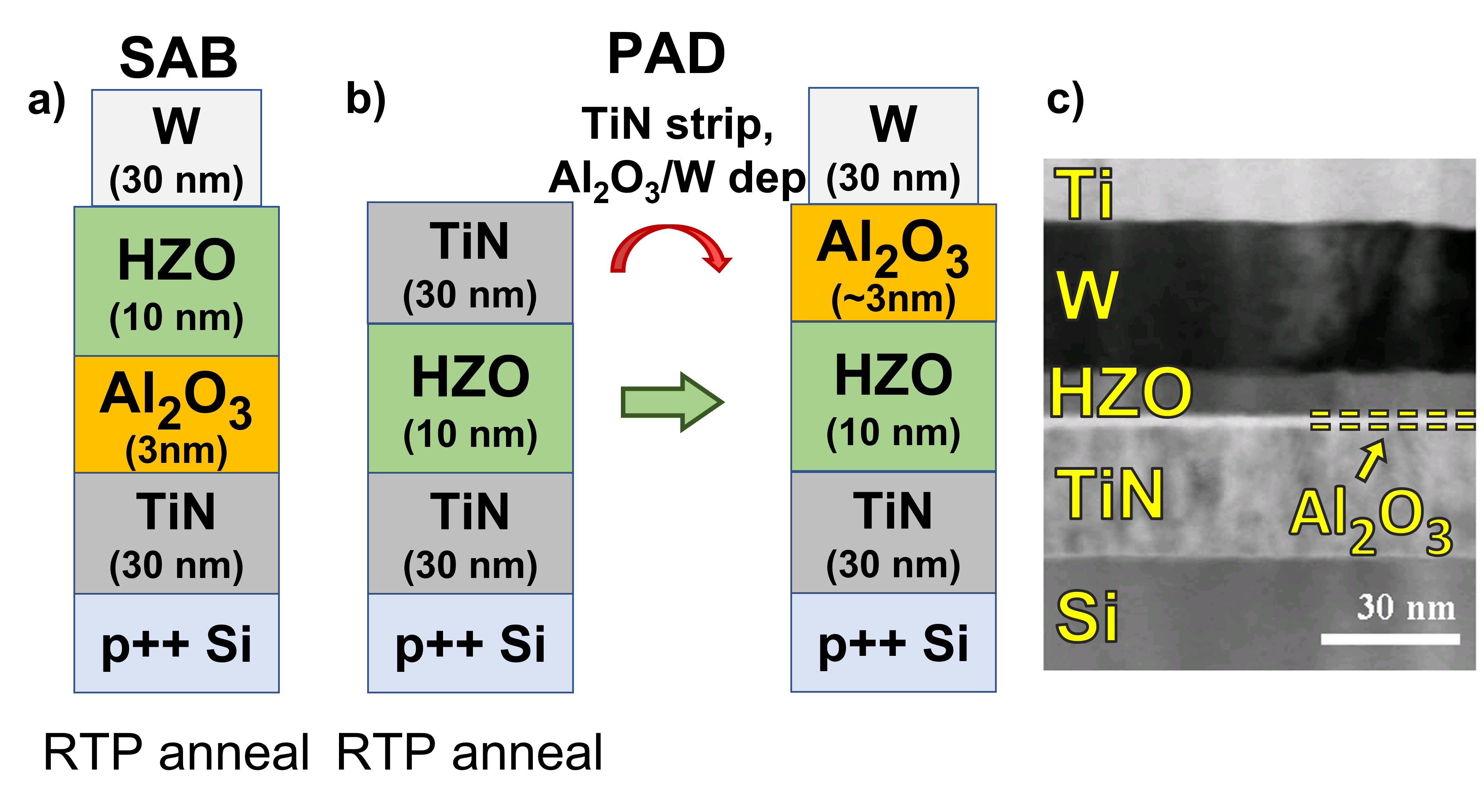
The field driven polarization switching and the tunneling read current qualify Ferroelectric Tunnel Junctions (FTJs) as high–impedance and low–energy synaptic devices. In this respect, in order to overcome the challenge of ultra–thin ferroelectric layers (1–3 nm) needed in Metal–Ferroelectric–Metal (MFM) stacks, the FTJ design has been recently steered towards Metal–Ferroelectric–Insulator–Metal (MFIM) devices (see Fig. 1), that are particularly suited for the integration in the BEOL of CMOS circuits [4, 5].
However, the operation of MFIM FTJs inherently relies on delicate trade–offs. In fact, the depolarization field enables a polarization dependent tunnelling read current, but it also tends to destabilize the polarization in retention and read mode. Moreover, in ferroelectric–dielectric (FE-DE) stacks the charge injection and trapping substantially influence the stability of polarization and its switching dynamics [6], as it has also been recognized and debated for ferroelectric–based FETs [7, 8, 9]. Clearly a simulation driven optimization of FTJs is necessary to meet the sometimes conflicting design targets. To this purpose, it is indispensable that a credible modelling framework for the FTJs is developed. This can only be achieved through an appropriate comparison and validation with experiments.
In this work we present an unprecedented joint effort based on an in–house developed numerical model and experiments to understand and to quantitatively investigate the trade–offs implied in the operation of FTJs as synaptic devices. The calibration of the simulator against experiments clarifies some crucial aspects of the device operation related to the charge trapping inside the MFIM stack. In particular, our results show that either a small or a very large trapping induce, respectively, negligible or complete compensation of the ferroelectric polarization, that hinder the FTJ operation in both cases. In this respect, we report optimal compensation conditions that can be exploited to optimize FTJs as synaptic devices with multiple conductance levels.
II Device fabrication and experiments
Two types of MFIM FTJ stacks were fabricated with the same nominal thickness for FE and DE films, but through different process sequences. The sketch of the devices is reported in Fig. 1. The first stack named ‘Stack Anneal–Bottom’ [SAB, Fig. 1a)] was fabricated as follows: a 30 nm TiN layer was sputtered on Si substrate as the bottom electrode, then a 3 nm Al2O3 film followed by a 10 nm Hf0.5Zr0.5O2 (HZO) layer were deposited by atomic layer deposition at 250∘C. Finally, a 30 nm W layer was deposited as top electrode by sputtering at room temperature. The entire stack underwent a crystallization anneal by RTP at 400∘C for 120 s in N2 ambient. The top electrodes were patterned by Ti/Pt lift–off followed by W etch in H2O2. A TEM image of a SAB FTJ is shown in Fig. 1c).
The second FTJ named ‘Post–Anneal Deposition’ [PAD, Fig. 1b)] was fabricated as follows. After the deposition of the 30 nm bottom TiN electrode onto the Si substrate, a 10 nm HZO layer followed by a 30 nm TiN film were first deposited. The obtained TiN/HZO/TiN stack was RTP annealed at 400∘C for 120 s in N2 ambient. After the anneal, the top TiN layer was completely etched away and the 3 nm Al2O3 film was deposited at 250∘C. The deposition and patterning of top W pads was then performed with the process described earlier for the SAB device. Note that, in the PAD FTJ case, the HZO was not in contact with the Al2O3 layer during annealing, while in the SAB stack the HZO and Al2O3 layers were annealed together. This is expected to lead to different HZO/Al2O3 interfaces in the two devices and, thus, to different chemical and electrical boundary conditions for the switching and stabilization of the HZO polarization. In particular, one may expect a significantly larger density of traps at the annealed HZO/Al2O3 interface of the SAB stack compared to the PAD case. TiN/HZO/TiN capacitors with a 10 nm HZO layer were also fabricated as a reference.
After fabrication, SAB and PAD FTJs are woken–up through 2000 cycles of a triangular waveform at 1 kHz with 4.5 V amplitude. The number of wake–up cycles corresponds to what is needed to wake–up the reference TiN/HZO/TiN capacitors. Then, polarization–voltage (P–V) and current–volage (I–V) loops are measured by applying 1 ms long triangular pulses to the top electrode, with the substrate at ground potential. To avoid the breakdown of devices, the maximum voltage amplitudes used for SAB and PAD FTJs are 5 and 4.5 V, respectively.
III Modelling framework and calibration
For the FTJ simulations, we used the in–house numerical model whose details can be found in [10, 11, 12]. In particular, the FE domain dynamics is solved through multi–domain Landau, Ginzburg, Devonshire (LGD) equations, accounting for the 3D electrostatics [10], whose only free parameters are the LGD constants , , , the resistivity of the FE dynamics (setting the time scale), and the domain wall coupling constant . In all simulations, we used m, consistently with the values recently reported for HZO based capacitors [13, 14, 15], and set in accordance with recent first principle calculations [16] and a detailed comparison between our model and transient operation of ferroelectric based devices [15].
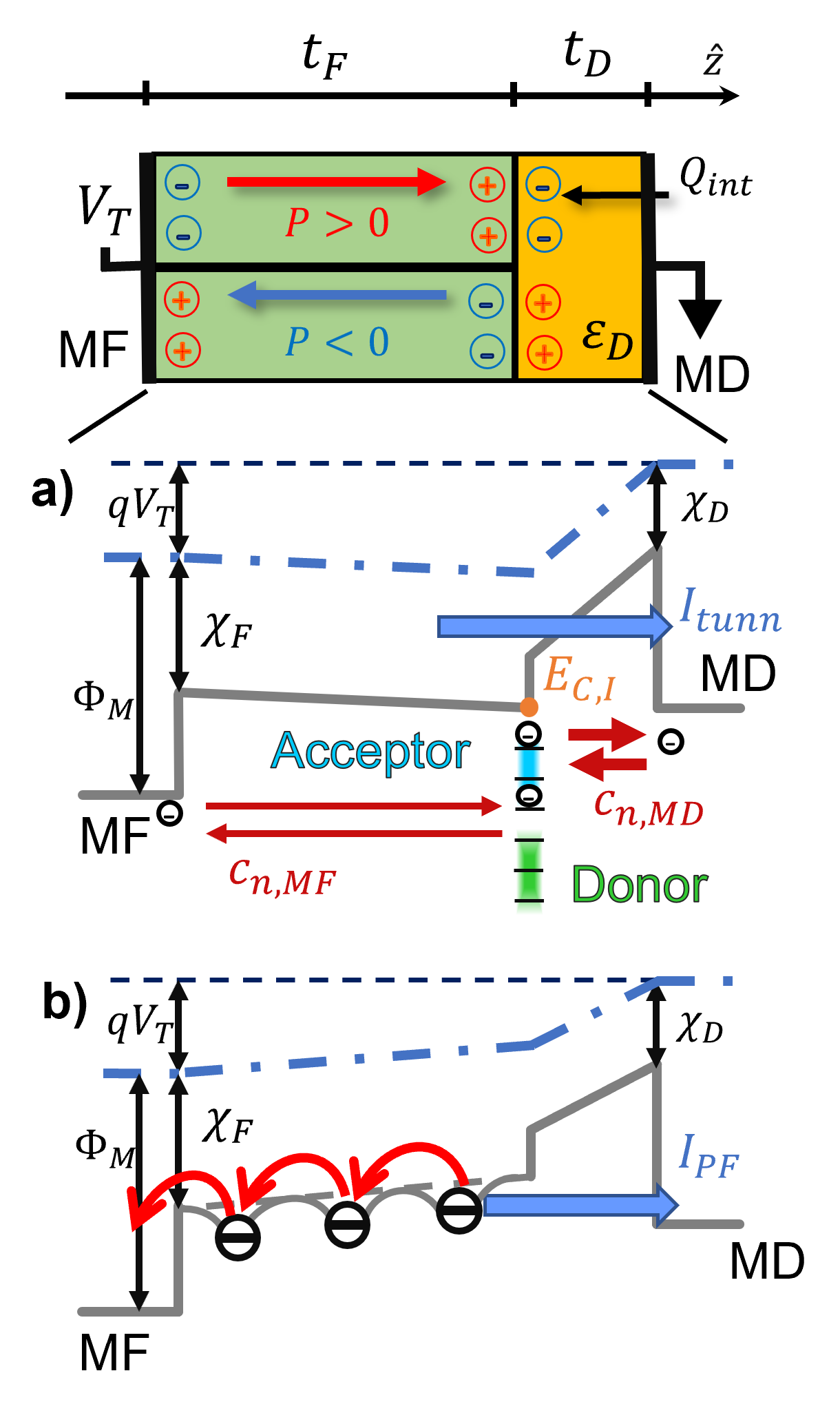
Concerning the read current, , it is assumed to be dominated by the tunnelling across the Al2O3 layer, even if additional mechanisms assisted by defects are also possible [17]. In this respect, Fig. 2 qualitatively shows that a similar band bending across the Al2O3 layer is necessary for either a current dominated by tunnelling (, a) or by a Poole–Frenkel mechanism in shallow HZO traps (, b).
The model also includes charge injection and trapping, which is described in terms of areal densities at the FE–DE interface [12]. However, it is acknowledged that the trap concentrations of this work should be considered as effective areal densities including also a possible charge trapping inside the FE and DE films. The model solves the trap occupation through first order dynamic equations for each trap energy level at the FE–DE surface, assuming a Fermi occupation functions in the metals MF and MD, respectively at the ferroelectric and dielectric side (see Fig. 2) [12]. A detailed balance condition ensures that the is given by the Fermi function at equilibrium (i.e. in steady state at V). As discussed above, the capture rates , from the MD and the MF electrodes, respectively, are attributed to tunnelling and depend on the area () and energy () cross sections of the traps. In each simulation domain the charges , in acceptor and donor traps, respectively, depend on and are proportional to the trap densities , . The trap dynamics are solved in all domains self–consistently with the LGD equations for the ferroelectric behaviour [12].
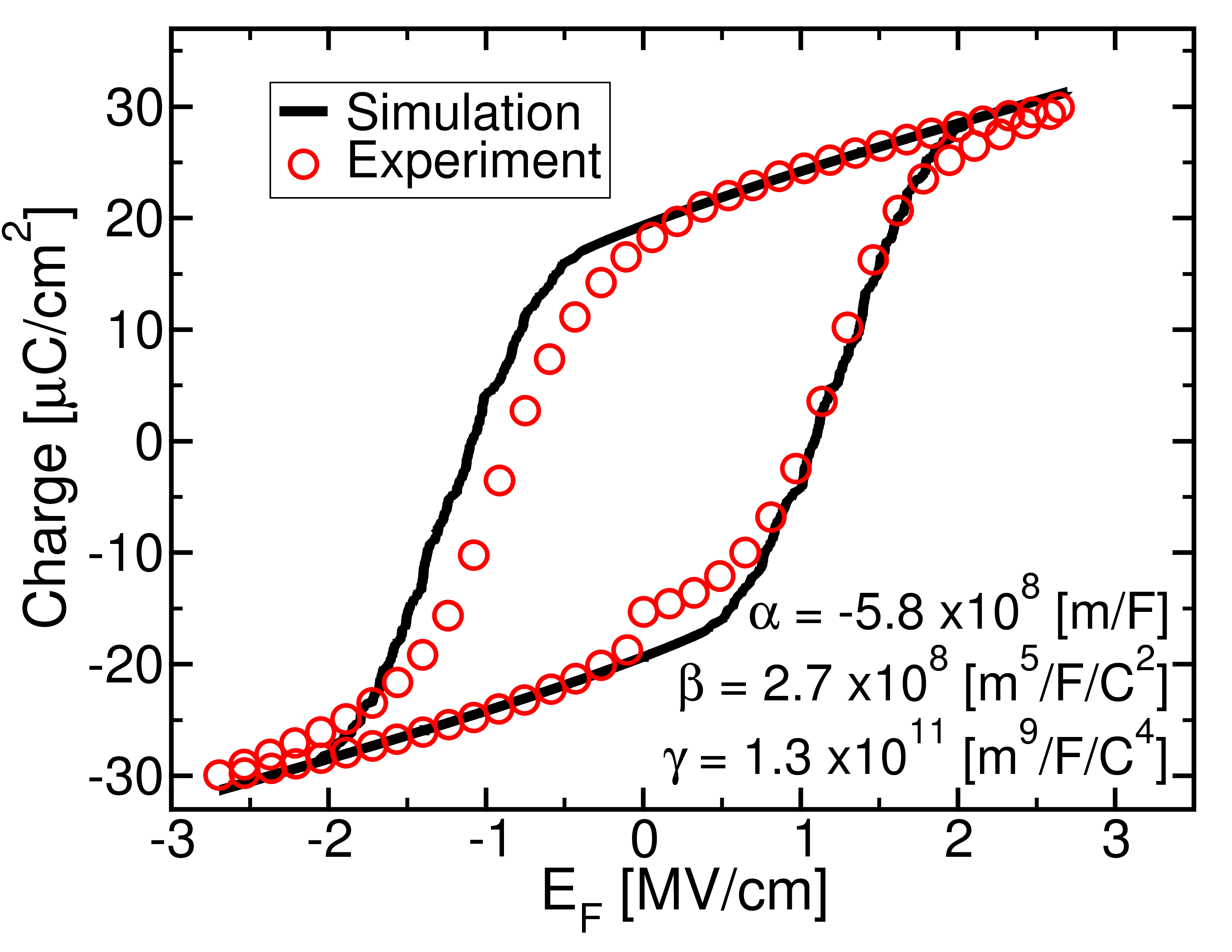
We calibrated the model against experiments. In Fig. 3 the simulations based on the LGD equations agree fairly well with the experimental charge versus electric field, , curve for a TiNHZOTiN structure, except for the slight asymmetry in the measured P–V. This could be due to differences in top and bottom TiN–HZO interfaces, that are not considered in the simulations. Such comparison allowed us to extract the LGD constants. In particular, in order to reproduce the experiments well, we considered domain–to–domain variations of the LGD parameters by assuming a normal distribution of , and . The mean values of such distributions are reported in Fig. 3, while the standard deviation of each constant are , and . Throughout this work, we will use these nominal values, if not otherwise stated.
In all simulations, the work functions of W and TiN electrodes were taken as 4.5 eV, while for the tunneling mass and the permittivity we assumed and for the HZO, and for the Al2O3, with being the free electron mass and the permittivity of vacuum. The values for these material parameters are empirically validated by the fairly good agreement between simulations and experiments.
IV Evidence of trap contribution in FTJ operation
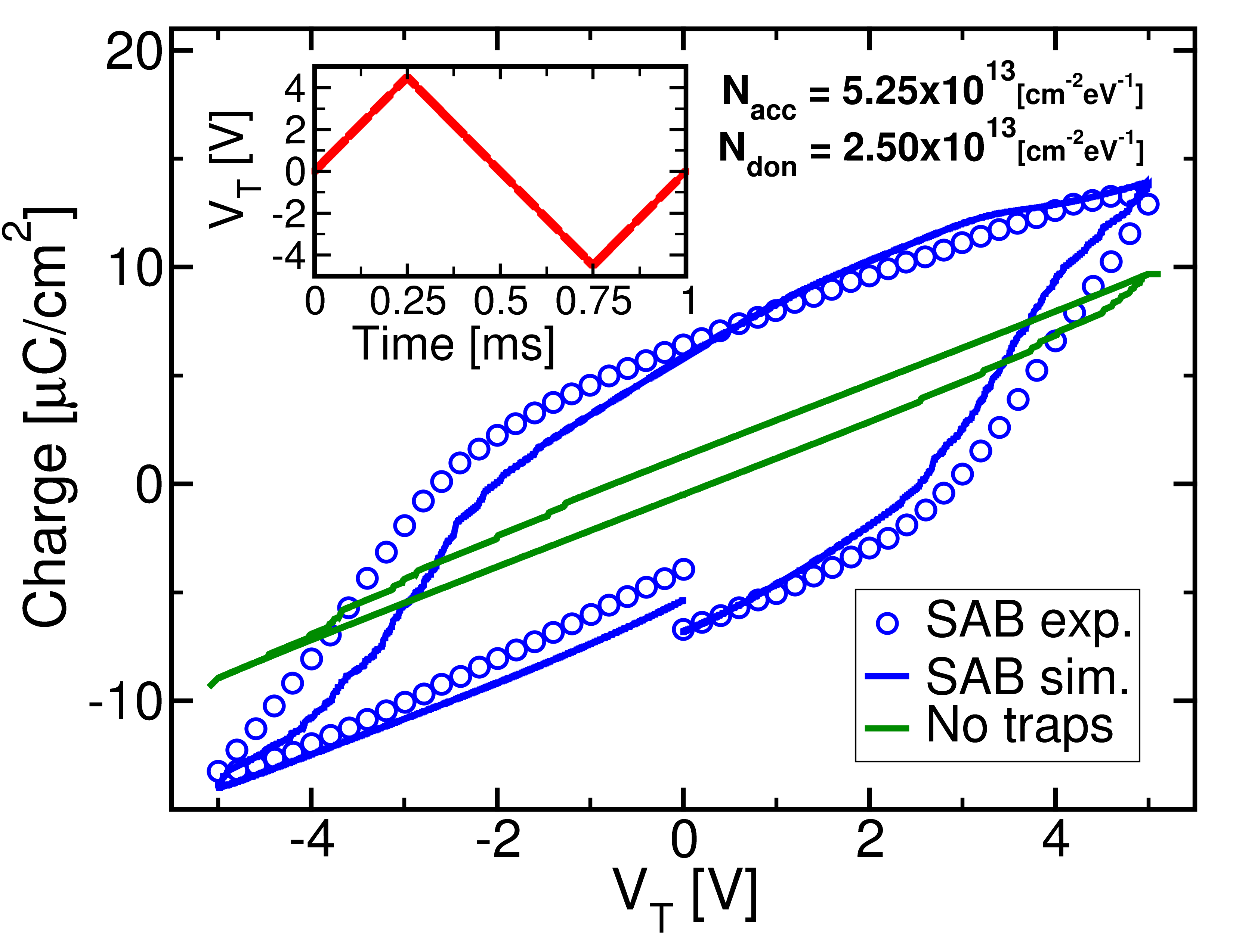
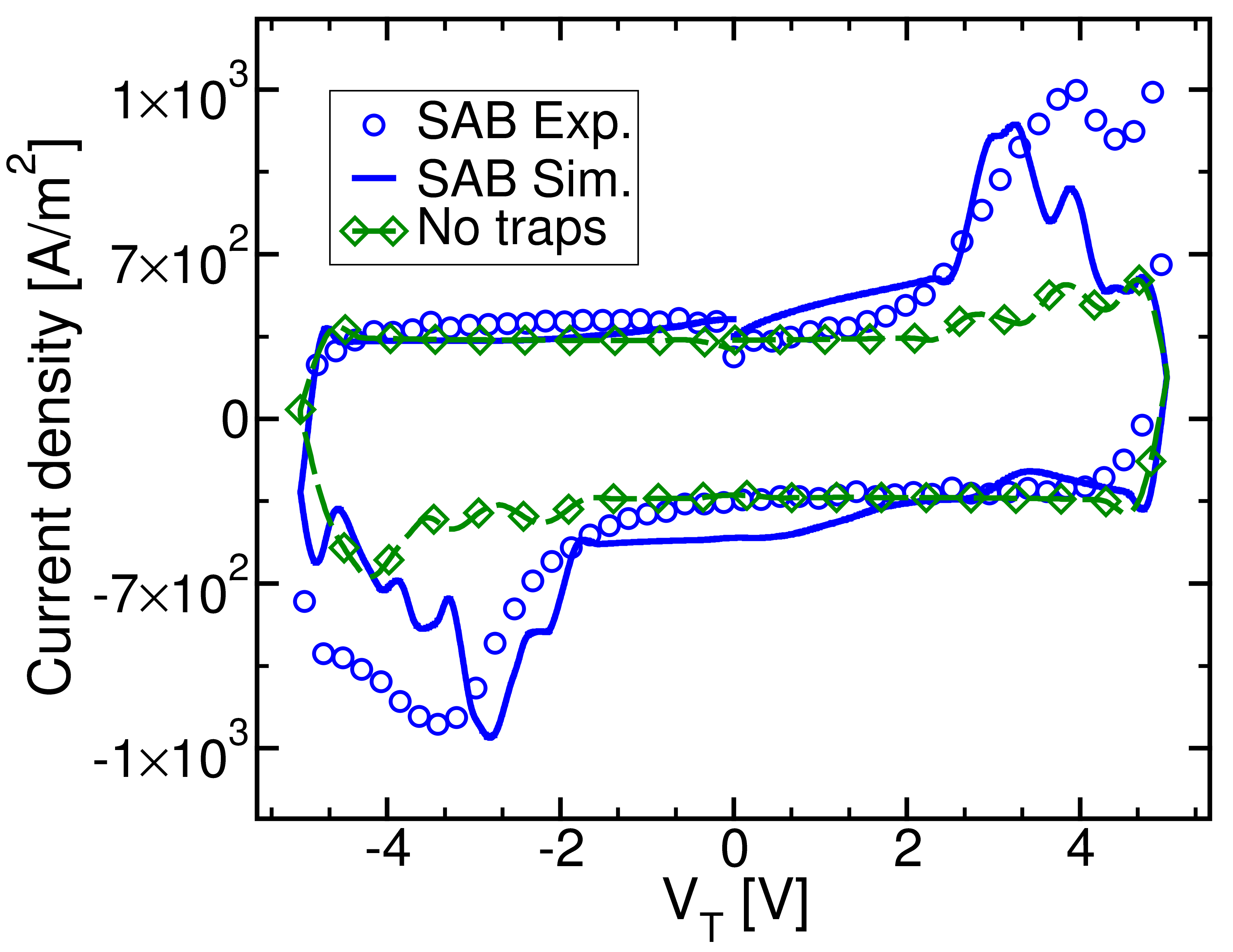
Figure 4 compares simulations and experiments concerning the polarization–voltage (–) curves of the SAB devices. As it can be seen, simulations neglecting charge injection and trapping (green line) exhibit a much more stretched – curves compared to experiments. These simulation results are actually qualitatively consistent with experiments reported for a HZO capacitor serially connected to a discrete ceramic capacitor ensuring zero charge injection [6, 18]. Similarly, in Fig. 5, also current–voltage (–) simulations hardly show any switching current when trapping is neglected.
A fairly good agreement with – and – experiments can instead be achieved by including, in the simulations, an adequate charge density at the FE–DE interface (see blue lines in Figs. 4 and 5). This is a clear evidence of the contribution of the charge trapping in the operation of FTJs, that is in line with recent results reported for FeFET devices [7, 8, 9]. It is worth mentioning that in Figs. 4, 5 and 6 the LGD constants had to be changed compared to Fig. 3, in order to increase the coercive field , thus improving the agreement with experiments. This increase of the apparent in MFIM compared to MFM structures has been previously reported and it has been ascribed to the division of external voltage between DE and FE layer. The capacitance of the ferroelectric increases as the field approaches , causing an increased drop across the DE layer and thus higher apparent than in MFM [19].
| SAB | |||||
|---|---|---|---|---|---|
| PAD |
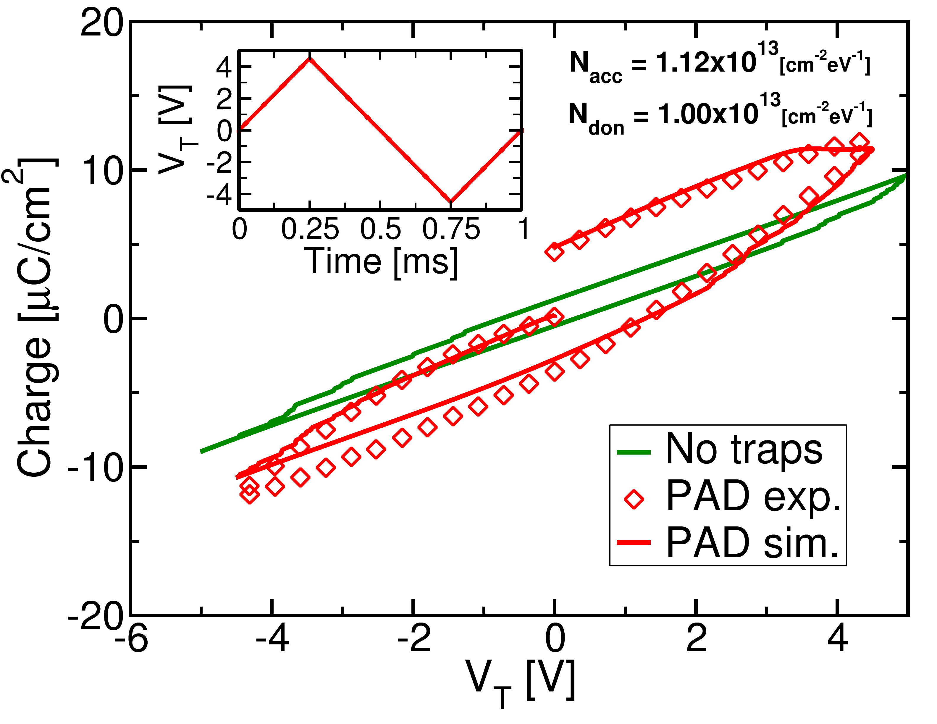
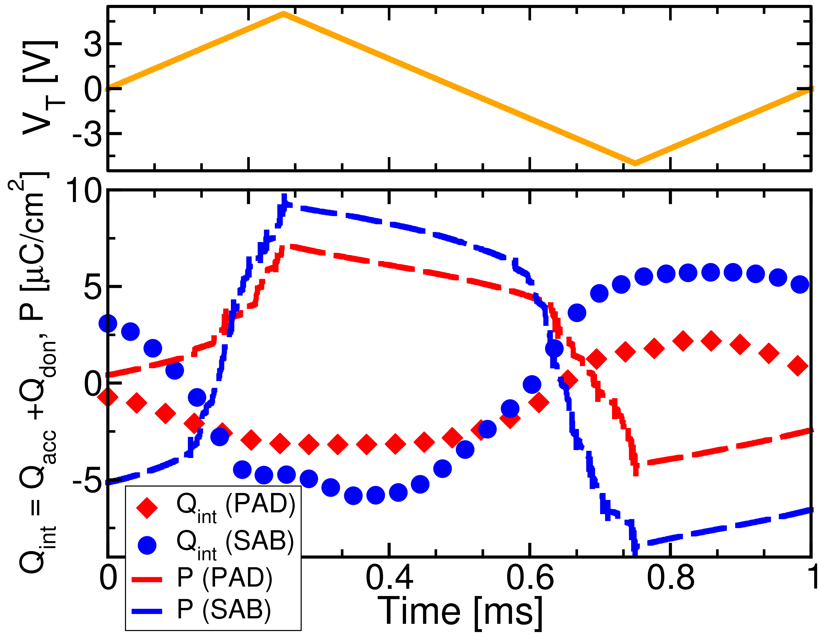
Figure 6 reports an analysis similar to that in Fig. 4 for the PAD devices. Even for the PAD FTJs, the simulations neglecting trapping (green line) exhibit large discrepancies with experiments (symbols). However, the trap density matching simulations with experiments is smaller than the concentration used for the SAB devices (see Tab. I). It should be mentioned that not only the processing conditions but also the FTJ wake–up may influence the density of the electrically active defects. However, since both FTJs underwent the same wake–up sequence, we expect that this difference is due to the different annealing conditions for the two devices. The difference in the simulated interfacial charge in SAB and PAD samples is best illustrated by Fig. 7, reporting the average polarization and trapped charge along a triangular waveform. Figure 7 shows that the polarization is partly compensated by in both devices, but the effect is more prominent in SAB FTJs. Again, this is ascribed to the different annealing sequence between the two devices and Fig. 7 provides an insight about the role of the trap density at the HZO/Al2O3 interface in the FTJ operation. At the present time we are not able to explore additional annealing conditions besides those employed for SAB and PAD devices. However, the conditions explored here are in the suitable range for the FTJ integration in a CMOS BEOL. This is an important aspect for the neuromorphic applications of FTJs, so that the paper is actually focused on BEOL compatible process conditions.
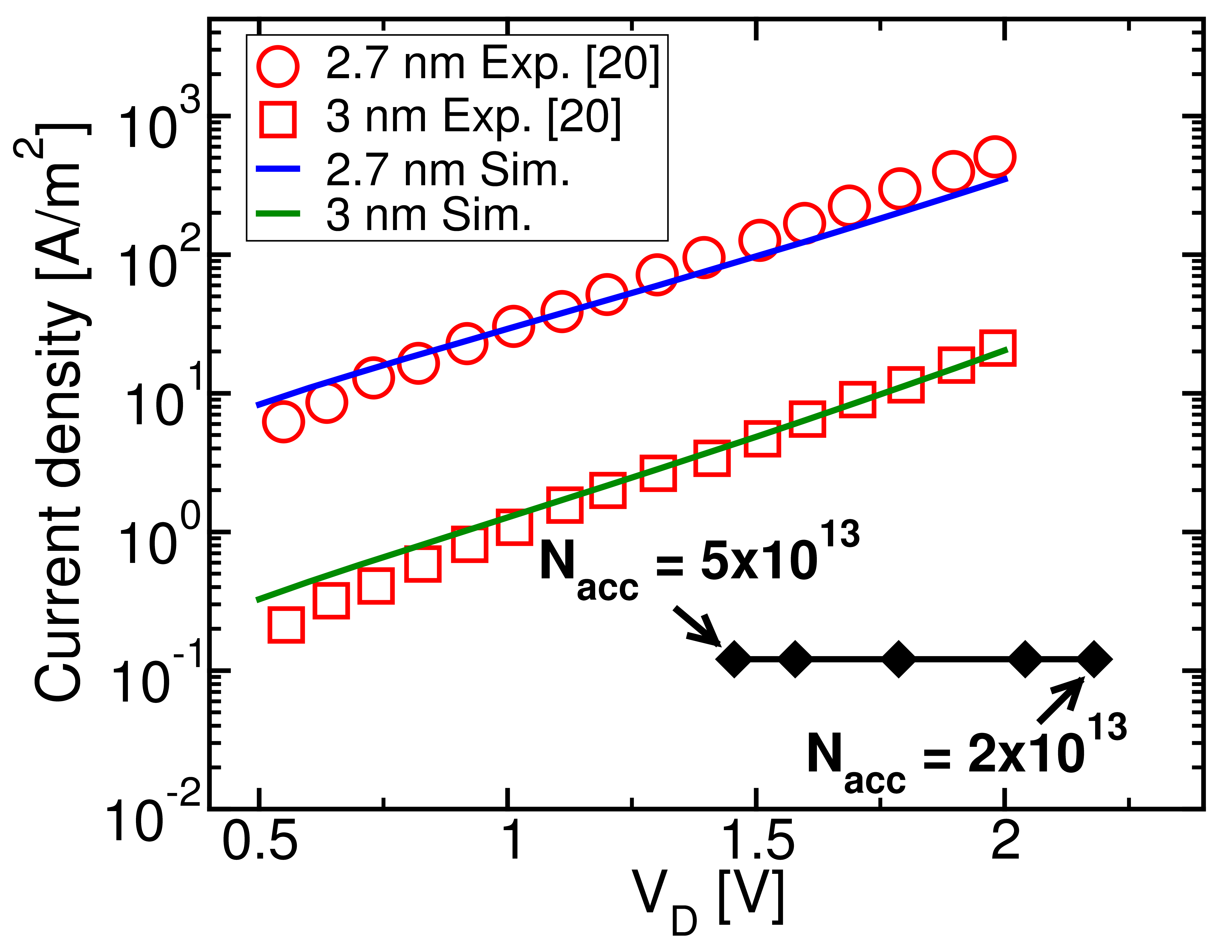
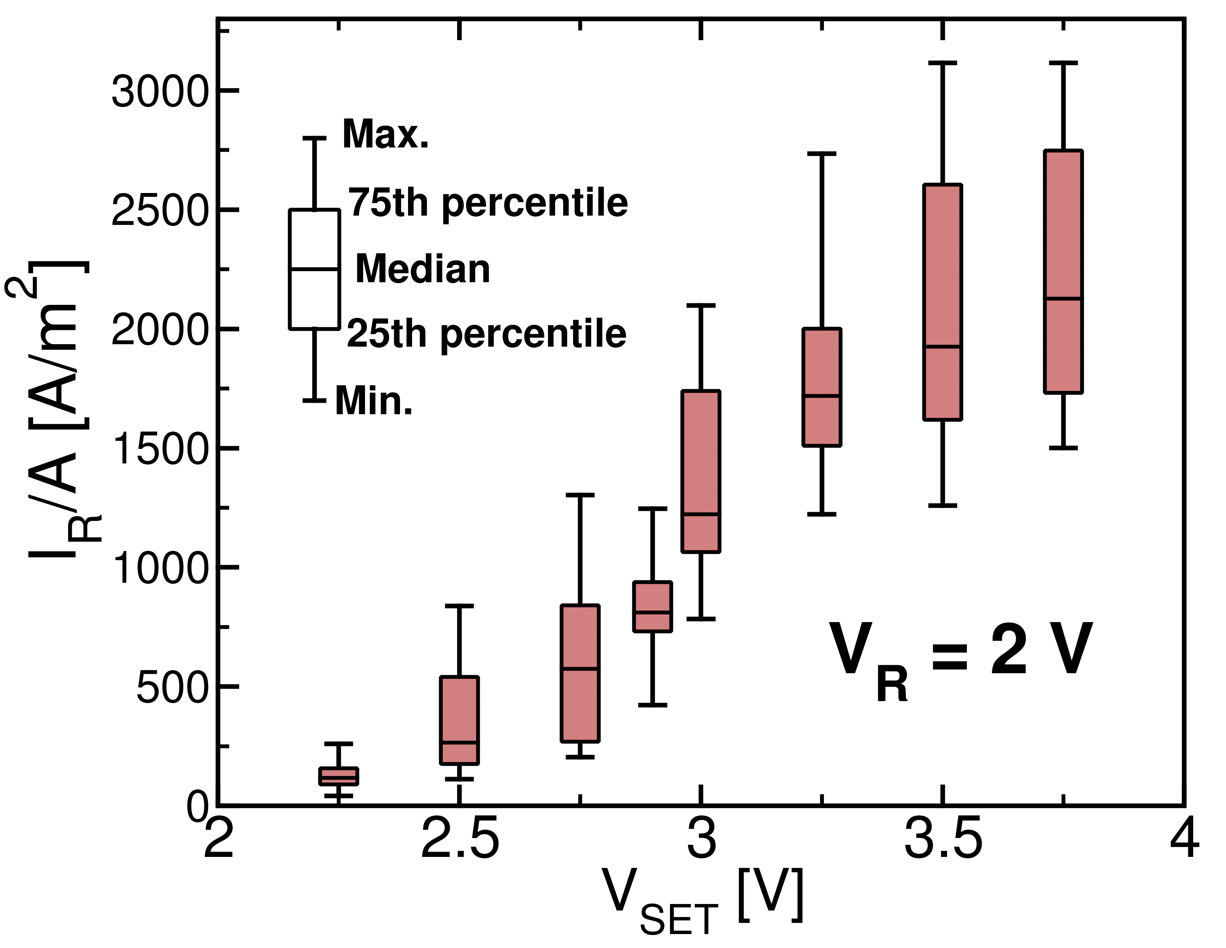
In read mode, the compensation of the positive polarization is expected to reduce the band bending and thus the read current (see Fig. 2). In this regard, Fig. 8 shows the measured ON current density of about 0.12 A/m2 (black diamonds) for SAB FTJs, together with the tunnelling current density in metal–SiO2–metal (MIM) systems [20]; incidentally, our tunnelling model is in good agreement with experiments in the MIM systems. For the FTJ device, the voltage drop, , across the Al2O3 layer is estimated by simulations and for different . Figure 8 shows that the estimated for cm-2eV-1 (see SAB parameters in Tab. I) is clearly smaller than the value V required to have a read current limited by the through the Al2O3 film alone [see Fig. 2a)]. Consistently with this picture, the measured is much smaller than the in MIM systems, and it may be limited by Poole–Frenkel conduction [see in Fig. 2b)].
V Polarization–compensation–aware design of the FTJ
In recent designs of neuromorphic processors, a reasonable target for the minimum read current is set to about 100 pA [21, 22], which requires a read current density of about A/m2 for an FTJ area of m2. Hereafter, we use our calibrated simulations to examine the optimal design of FTJs in terms of and tunneling electroresistance TER . For the simulations in this section, the LGD constants are those in Fig. 3, calibrated on the MFM device, in order to precisely account for the characteristics of the integrated HZO layer.
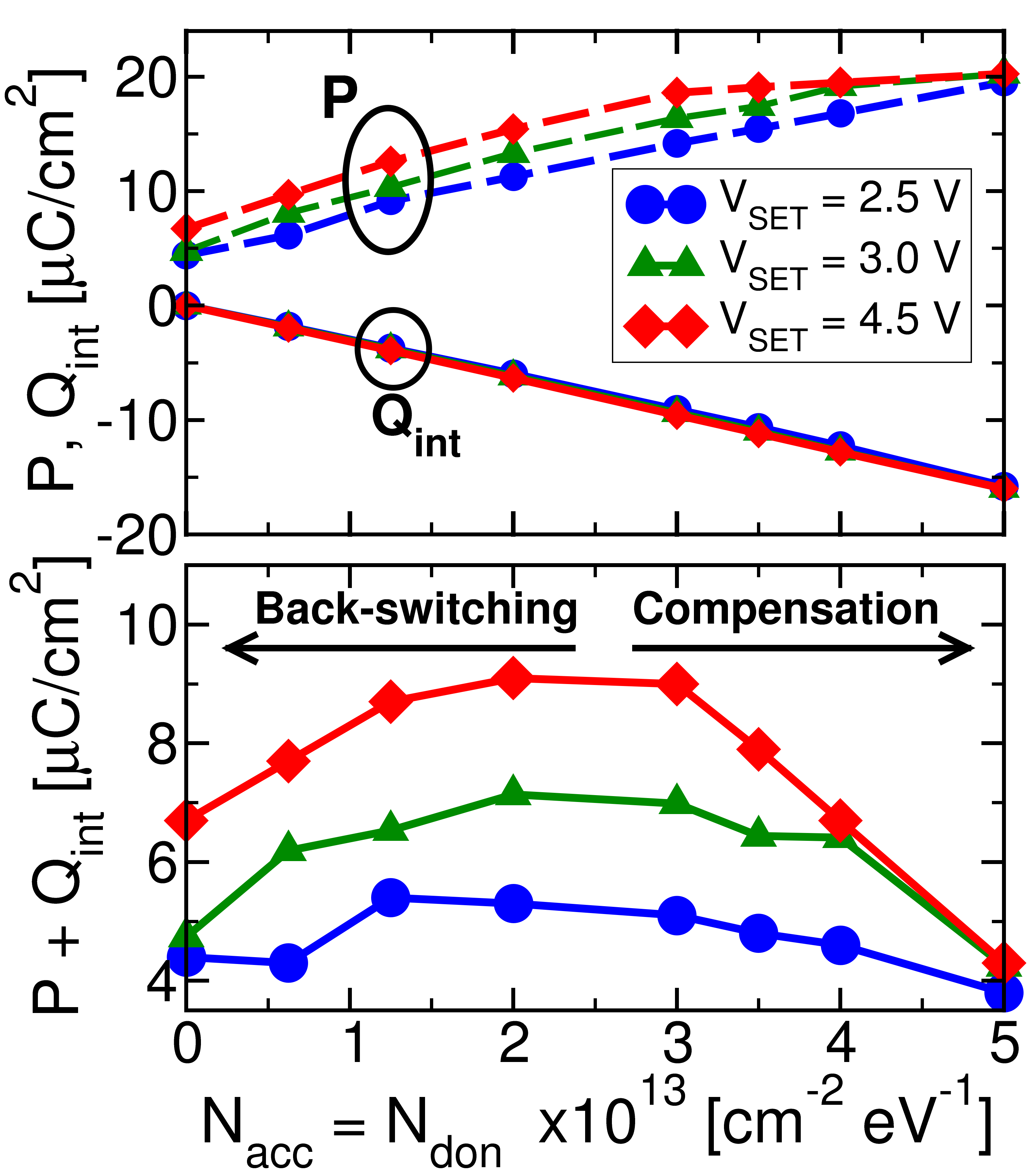
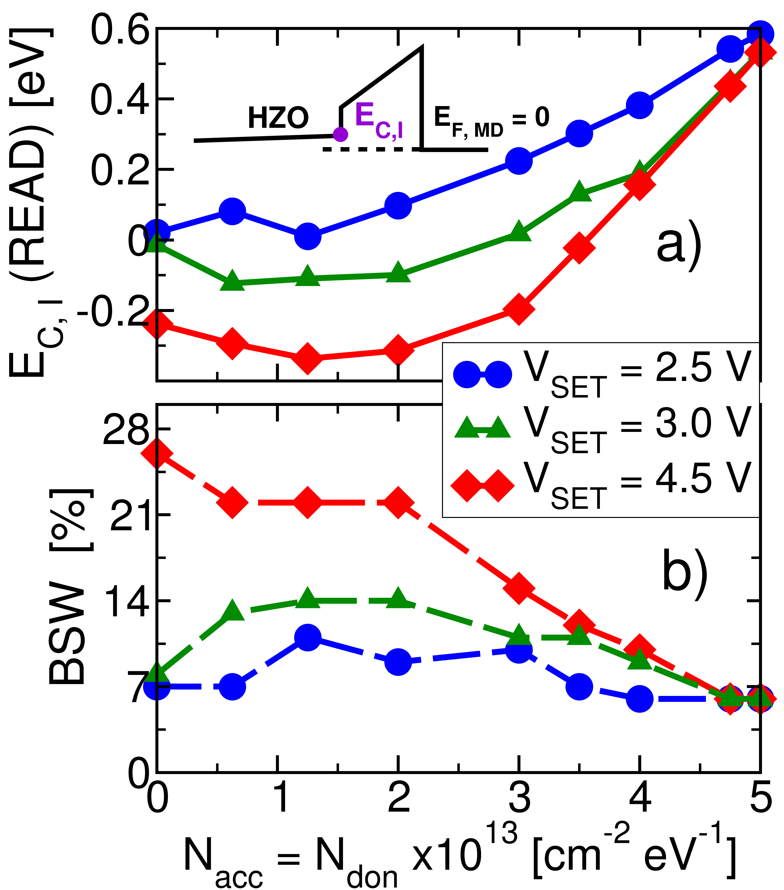
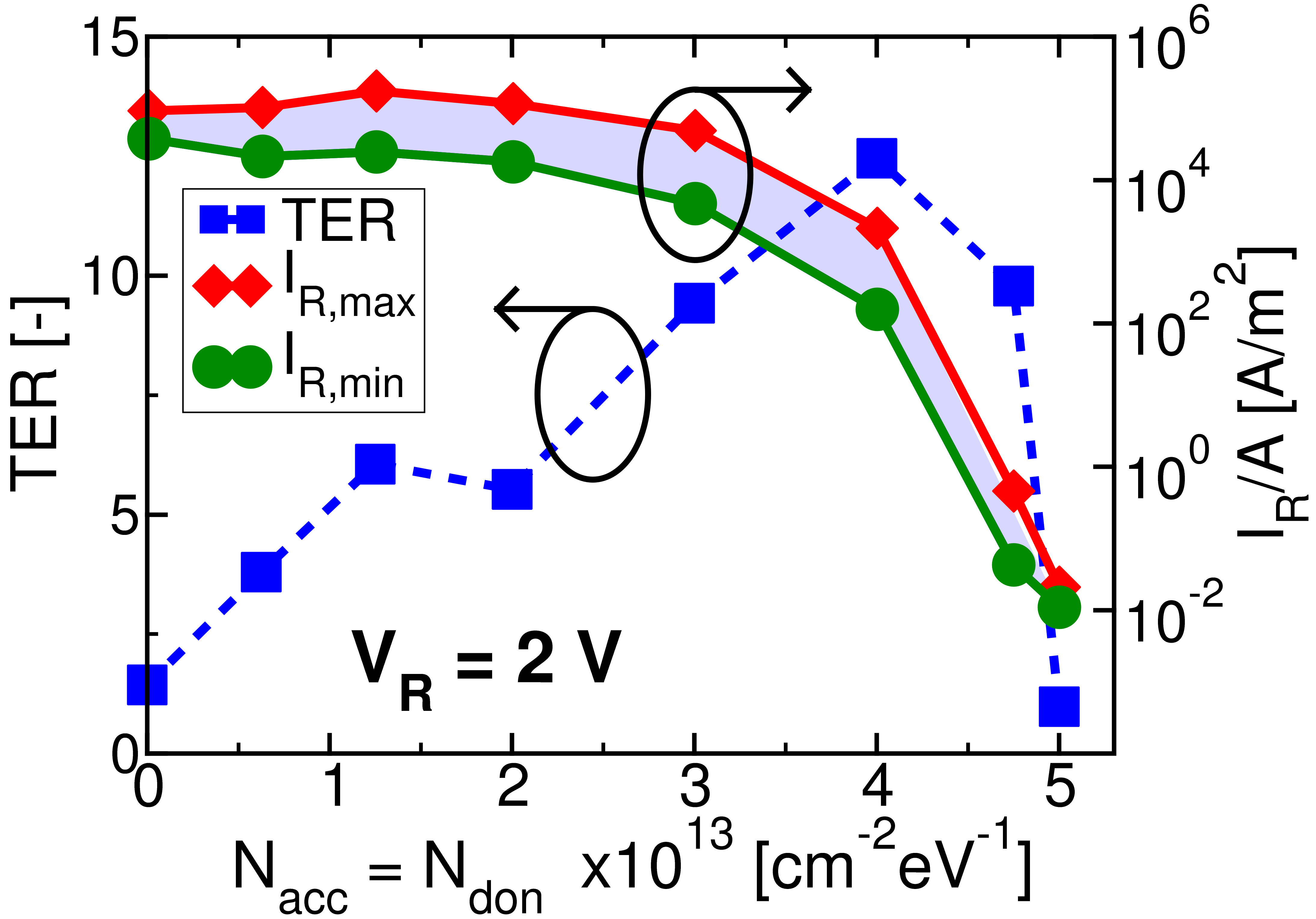
Figure 9 reports the simulated minimum and maximum read current densities and TER for a FTJ having an Al2O3 thickness scaled down to nm and for different trap densities 111This simplifying assumption of an equal density of acceptor and donor traps has been introduced in order to limit the number of free parameters in the analysis carried out in this section. We expect that the main outcome of this discussion does not change if and are allowed to be different.. Despite the uncertainties that admittedly affect our calculations of the read current and have been also discussed in Fig. 8, the and the TER values calculated at large trap densities are in–line with recent literature on SoA FTJ devices, showing read currents in the 0.05–0.6 A/m2 range and TER values between 5 and 12.5 [23, 24, 25].
Quite interestingly, Figure 9 shows that the TER exhibits an optimal value for around cm-2eV-1, which stems from the behavior of the net or compensated polarization illustrated in Fig. 10. In fact, at low values, the compensation of the positive is too weak, so that the depolarization field increases and destabilizes the polarization. In this respect, we calculated the difference between the number of domains with positive spontaneous polarization at the maximum value of the SET voltage and at zero external bias (i.e. during retention) and then we divided this value by the overall number of domains. This is indeed the fraction of the domains set to positive during the SET pulse that back–switch to negative during retention. We defined such value as back–-switching in Fig. 11b), which shows that at low a significant back–switching of the ferroelectric domains occurs. The large back–-switching at low deteriorates the TER in Fig. 9.
At large , instead, there is an excessive compensation that reduces . This implies an increase of the HZO conduction band minimum, , at the FE–DE interface during the read mode, which is reported in Fig. 11a). Such an raise leads to the large drop at high shown in Fig. 9. Moreover, a large compensation tends to merge the states obtained by different values, which seriously hinders a multi–level read current and thus the operation as a synaptic device.
The results of Fig. 9 and the inspection of the internal quantities performed in Figs. 10 and 11, clearly show that an optimal compensation condition exists for the operation of FTJs. In this respect, as discussed above, both negligible and excessive charge–trapping–induced compensation of the ferroelectric polarization are detrimental for the operation of the FTJs under study. Indeed, there exists a quite delicate balance between the suppression of back–switching and TER values enabling a multi–level operation in read mode. In Fig. 12, for a given FTJ structure, we leverage the optimal design condition in Fig. 9 and show that eight current levels can be placed in the memory window of the FTJ for the optimal compensation condition corresponding to cm-2eV-1, thus enabling a 3–bit synaptic weight resolution. It is worth mentioning that such an optimal condition corresponds to a across the Al2O3 layer that is very close to or larger than the value V required to have tunnelling through the thin dielectric film alone [see Figs. 2a) and 11]. A comparison of the calculated with experiments suggests that it is probably difficult in actual FTJs to reach this favourable condition where is only limited by the tunnelling through the Al2O3 layer, as also discussed in Fig. 8.
VI Conclusions
We presented a joint effort between numerical modelling and experiments to demonstrate the crucial role of polarization compensation due to trapped charges in HZO based FTJs. We identified and physically explained the optimal compensation condition for a robust operation of FTJs.
Even if a tailoring of trap densities may be challenging from a technological standpoint, we experimentally demonstrated that appropriate processing steps and annealing conditions can lead to different trap densities at the FE–DE interface of fabricated FTJs. Moreover, the trap density can be partly controlled in ALD deposited Al2O3 films by tuning the deposition parameters such as the precursor pulse duration, the oxidant precursor type (water, O2 plasma, ozone), the deposition temperature, and the dosing time. These processing parameters have been shown to change the Al2O3 defect density at least by an order of magnitude [26, 27, 28]. Another pathway is to include an ultrathin charge trap layer between the tunneling dielectric and HZO [29]. As a final remark, the insertion of an ultra–thin metal layer at the FE–DE interface may also be an interesting design option to control the compensation condition in FTJs, as it has been suggested in [30].
Acknowledgment
The authors thank Dr. A. Hammud, FHI–Berlin, for support.
References
- [1] S. Yu, “Neuro-inspired computing with emerging nonvolatile memorys,” Proceedings of the IEEE, vol. 106, no. 2, pp. 260–285, 2018. doi: 10.1109/JPROC.2018.2790840
- [2] S. Ambrogio, P. Narayanan, H. Tsai, R. M. Shelby, I. Boybat, C. di Nolfo, S. Sidler, M. Giordano, M. Bodini, N. C. P. Farinha, B. Killeen, C. Cheng, Y. Jaoudi, and G. W. Burr, “Equivalent-accuracy accelerated neural-network training using analogue memory,” Nature, vol. 558, no. 7708, pp. 60–67, Jun 2018. doi: 10.1038/s41586-018-0180-5
- [3] E. Chicca and G. Indiveri, “A recipe for creating ideal hybrid memristive-cmos neuromorphic processing systems,” Applied Physics Letters, vol. 116, no. 12, p. 120501, 2020. doi: 10.1063/1.5142089. [Online]. Available: https://doi.org/10.1063/1.5142089
- [4] S. Slesazeck and T. Mikolajick, “Nanoscale resistive switching memory devices: a review,” Nanotechnology, vol. 30, no. 35, p. 352003, jun 2019. doi: 10.1088/1361-6528/ab2084. [Online]. Available: https://doi.org/10.1088/1361-6528/ab2084
- [5] R.Fontanini, J.Barbot, M.Segatto, S.Lancaster, Q.Duong, F.Driussi, L.Grenouillet, F.Triozon, J.Coignus, T.Mikolajick, S.Slesazeck, and D. Esseni, “Polarization switching and interface charges in BEOL compatible ferroelectric tunnel junctions,” in 2021 IEEE 51st European Solid-State Device Research Conference (ESSDERC), 2021.
- [6] H. W. Park, S. D. Hyun, I. S. Lee, S. H. Lee, Y. B. Lee, M. Oh, B. Y. Kim, S. G. Ryoo, and C. S. Hwang, “Polarizing and depolarizing charge injection through a thin dielectric layer in a ferroelectric–dielectric bilayer,” Nanoscale, vol. 13, pp. 2556–2572, 2021. doi: 10.1039/D0NR07597C
- [7] K. Toprasertpong, M. Takenaka, and S. Takagi, “Direct observation of interface charge behaviors in FeFET by quasi-static split C-V and hall techniques: Revealing FeFET operation,” in 2019 IEEE International Electron Devices Meeting (IEDM), 2019. doi: 10.1109/IEDM19573.2019.8993664 pp. 23.7.1–23.7.4.
- [8] J. Li, Y. Qu, M. Si, X. Lyu, and P. D. Ye, “Multi-Probe characterization of ferroelectric/dielectric interface by C-V, P-V and conductance methods,” in 2020 IEEE Symposium on VLSI Technology, 2020. doi: 10.1109/VLSITechnology18217.2020.9265069 pp. 1–2.
- [9] S. Deng, Z. Jiang, S. Dutta, H. Ye, W. Chakraborty, S. Kurinec, S. Datta, and K. Ni, “Examination of the interplay between polarization switching and charge trapping in Ferroelectric FET,” in 2020 IEEE International Electron Devices Meeting (IEDM), 2020. doi: 10.1109/IEDM13553.2020.9371999 pp. 4.4.1–4.4.4.
- [10] T. Rollo, F. Blanchini, G. Giordano, R. Specogna, and D. Esseni, “Stabilization of negative capacitance in ferroelectric capacitors with and without a metal interlayer,” Nanoscale, vol. 12,, pp. 6121–6129, 2020. doi: 10.1039/c9nr09470a
- [11] R. Fontanini, M. Massarotto, R. Specogna, F. Driussi, M. Loghi, and D. Esseni, “Modelling and design of ftjs as high reading-impedance synaptic devices,” in 2021 5th IEEE Electron Devices Technology Manufacturing Conference (EDTM), 2021. doi: 10.1109/EDTM50988.2021.9420863 pp. 1–3.
- [12] R. Fontanini, M. Segatto, M. Massarotto, R. Specogna, F. Driussi, M. Loghi, and D. Esseni, “Modeling and design of ftjs as multi-level low energy memristors for neuromorphic computing,” IEEE Journal of the Electron Devices Society, vol. 9, pp. 1202–1209, 2021. doi: 10.1109/JEDS.2021.3120200
- [13] M. Kobayashi, N. Ueyama, K. Jang, and T. Hiramoto, “Experimental Study on Polarization-Limited Operation Speed of Negative Capacitance FET with Ferroelectric HfO2,” in 2016 IEEE International Electron Devices Meeting (IEDM), Dec 2016, pp. 314–317.
- [14] J. A. T. Kim and D. A. Antoniadis, “Dynamics of HfZrO2 ferroelectric structures: Experiments and models,” in 2020 IEEE International Electron Devices Meeting (IEDM), Dec 2020, pp. 441–444.
- [15] D. Esseni and R. Fontanini, “Macroscopic and microscopic picture of negative capacitance operation in ferroelectric capacitors,” Nanoscale, vol. 13, pp. 9641–9650, 2021. doi: 10.1039/D0NR06886A
- [16] H.-J. Lee, M. Lee, K. Lee, J. Jo, H. Yang, Y. Kim, S. C. Chae, U. Waghmare, and J. H. Lee, “Scale-free ferroelectricity induced by flat phonon bands in HfO2,” vol. 369, no. 6509, p. 1343–1347, 2020. doi: 10.1126/science.aba0067
- [17] H. Schroeder, “Poole-Frenkel-effect as dominating current mechanism in thin oxide films—An illusion?!” Journal of Applied Physics, vol. 117, no. 21, p. 215103, 2015. doi: 10.1063/1.4921949. [Online]. Available: https://doi.org/10.1063/1.4921949
- [18] M. Hoffmann, M. Gui, S. Slesazeck, R. Fontanini, M. Segatto, D. Esseni, and T. Mikolajick, “Intrinsic nature of negative capacitance in multidomain Hf0.5Zr0.5O2-based ferroelectric/dielectric heterostructures,” Advanced Functional Materials, vol. 32, no. 2, p. 2108494, 2022. doi: https://doi.org/10.1002/adfm.202108494. [Online]. Available: https://onlinelibrary.wiley.com/doi/abs/10.1002/adfm.202108494
- [19] L. Jiang, W. Hu, Z. Wei, W. Xu, and H. Meng, “High-performance organic single-crystal transistors and digital inverters of an anthracene derivative,” Advanced Materials, vol. 21, no. 36, pp. 3649–3653, 2009. doi: https://doi.org/10.1002/adma.200900503. [Online]. Available: https://onlinelibrary.wiley.com/doi/abs/10.1002/adma.200900503
- [20] N. Matsuo, T. Miura, A. Urakami, and T. Miyoshi, “Analysis of direct tunneling for thin SiO2 film,” Japanese Journal of Applied Physics, vol. 38, no. Part 1, No. 7A, pp. 3967–3971, jul 1999. doi: 10.1143/jjap.38.3967. [Online]. Available: https://doi.org/10.1143/jjap.38.3967
- [21] N. Qiao and G. Indiveri, “Scaling mixed-signal neuromorphic processors to 28 nm FD-SOI technologies,” in 2016 IEEE Biomedical Circuits and Systems Conference (BioCAS), 2016. doi: 10.1109/BioCAS.2016.7833854 pp. 552–555.
- [22] M. Sharifshazileh, K. Burelo, T. Fedele, J. Sarnthein, and G. Indiveri, “A neuromorphic device for detecting high-frequency oscillations in human iEEG,” in 2019 26th IEEE International Conference on Electronics, Circuits and Systems (ICECS), 2019. doi: 10.1109/ICECS46596.2019.8965192 pp. 69–72.
- [23] B. Max, M. Hoffmann, S. Slesazeck, and T. Mikolajick, “Direct correlation of ferroelectric properties and memory characteristics in ferroelectric tunnel junctions,” IEEE Journal of the Electron Devices Society, vol. 7, pp. 1175–1181, 2019. doi: 10.1109/JEDS.2019.2932138
- [24] H. Ryu, H. Wu, F. Rao, and W. Zhu, “Ferroelectric tunneling junctions based on aluminum oxide/ zirconium-doped hafnium oxide for neuromorphic computing,” Scientific Reports, vol. 9, no. 1, p. 20383, Dec 2019. doi: 10.1038/s41598-019-56816-x. [Online]. Available: https://doi.org/10.1038/s41598-019-56816-x
- [25] J. Hur, Y.-C. Luo, P. Wang, N. Tasneem, A. I. Khan, and S. Yu, “Ferroelectric tunnel junction optimization by plasma-enhanced atomic layer deposition,” in 2020 IEEE Silicon Nanoelectronics Workshop (SNW), 2020. doi: 10.1109/SNW50361.2020.9131649 pp. 11–12.
- [26] M. M. Rahman, K.-Y. Shin, and T.-W. Kim, “Characterization of electrical traps formed in Al2O3 under various ALD conditions,” Materials, vol. 13, no. 24, 2020. doi: 10.3390/ma13245809. [Online]. Available: https://www.mdpi.com/1996-1944/13/24/5809
- [27] J. B. Kim, D. R. Kwon, K. Chakrabarti, C. Lee, K. Y. Oh, and J. H. Lee, “Improvement in Al2O3 dielectric behavior by using ozone as an oxidant for the atomic layer deposition technique,” Journal of Applied Physics, vol. 92, no. 11, pp. 6739–6742, 2002. doi: 10.1063/1.1515951. [Online]. Available: https://doi.org/10.1063/1.1515951
- [28] K. Henkel, M. Kot, and D. Schmeißer, “Localized defect states and charge trapping in atomic layer deposited-Al2O3 films,” Journal of Vacuum Science & Technology A, vol. 35, no. 1, p. 01B125, 2017. doi: 10.1116/1.4971991. [Online]. Available: https://doi.org/10.1116/1.4971991
- [29] J.-Y. Wu, Y.-T. Chen, M.-H. Lin, and T.-B. Wu, “Ultrathin HfON trapping layer for charge-trap memory made by Atomic Layer Deposition,” IEEE Electron Device Letters, vol. 31, no. 9, pp. 993–995, 2010. doi: 10.1109/LED.2010.2052090
- [30] D. J. Frank, P. M. Solomon, C. Dubourdieu, M. M. Frank, V. Narayanan, and T. N. Theis, “The Quantum Metal Ferroelectric Field-Effect Transistor,” IEEE Transactions on Electron Devices, vol. 61, no. 6, pp. 2145–2153, 2014. doi: 10.1109/TED.2016.2614432