How to produce spin-splitting in antiferromagnetic materials
Abstract
Antiferromagnetic (AFM) materials have potential advantages for spintronics due to their robustness, ultrafast dynamics, and magnetotransport effects. However, the missing spontaneous polarization and magnetization hinders the efficient utilization of electronic spin in these AFM materials. Here, we propose a simple way to produce spin-splitting in AFM materials by making the magnetic atoms with opposite spin polarization locating in the different environment (surrounding atomic arrangement), which does not necessarily require the presence of spin-orbital coupling (SOC). We confirm our proposal by four different types of two-dimensional (2D) AFM materials within the first-principles calculations. Our works provide a intuitional design principle to find or produce spin-splitting in AFM materials.
I Introduction
The spin-orbit-coupling (SOC)-induced spin splitting have formed the basis for the development of spintronics within potential applications to spin transistor, spin-orbit torque, spin Hall effect, topological insulators, and Majorana Fermionsss1 . However, the rapid decoherence of spin-polarized electrons induced by SOC limit the widespread applications of these materialsss2 .The unidirectional spin-orbit field orientation can produce a spatially periodic mode of the spin polarization, which is known as the persistent spin helix (PSH)p7 ; p8 . The PSH can give rise to an extremely long spin lifetime by suppressing spin dephasing due to SU(2) spin rotation symmetryp7 ; p9 . To produce obvious spin splitting, these materials should incorporate heavy elements with the rarity, instability and toxicity. So, an alternative strategy should be used to realize spin splitting in the absence of SOC.
The Zeeman spin splitting in ferromagnets is irrelevant to SOC, and can be produced even when SOC is turned off. Any magnetic compound that has nonzero net magnetization can give rise to spin splitting with underlying Zeeman mechanism. A typical example is half-metallic ferromagnet, which possesses 100 % spin-polarized currentss3 . Superior to ferromagnetic (FM) materials, the antiferromagnetic (AFM) materials have attracted considerable research interest, since they are robust to external magnetic perturbation due to missing any net magnetic momentk1 ; k2 . In general, there are not spin splitting in the band structures in these antiferromagnets.

However, the altermagnetism with collinear symmetry-compensated antiferromagnetism can realize the spin splitting, where the SOC is not neededk4 ; k5 ; k6 . The altermagnetism is characterized by crystal-rotation symmetries connecting opposite-spin sublattices separated in the real space, which leads to opposite-spin electronic states separated in the momentum space. Several bulk materials and two-dimensional (2D) materials have been predicted to be altermagnetism, such as k7 , k7-1 , MnTek7-2 , some organic AFMsk8 , k9 , some -type perovskitesk10 , k11 ; k12 , k12-1 and k13 . Recently, a new mechanism has been proposed to achieve spin splitting in AFM materialsk14 . For a 2D material, the magnetic atoms have opposite layer spin polarization (A-type AFM ordering) with an out-of-plane built-in electric field, which can destroy the degeneration of electron spin in the band structures, called electric-potential-difference antiferromagnetism (EPD-AFM). Janus monolayer is proved to be a possible candidate to achieve the EPD-AFM by the first-principles calculationsk14 .
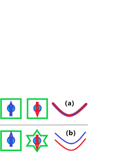
Is there an intuitive way to search for or produce spin splitting in AFM materials? Here, a simple way is proposed to produce spin-splitting in AFM materials. For antiferromagnetic materials: if the magnetic atoms with opposite spin polarization have the same environment (surrounding atomic arrangement), the degeneration of electron spin can be observed (see Figure 1 (a)); if the magnetic atoms with opposite spin polarization have different environment, the degeneration of electron spin can be removed (see Figure 1 (b)). For altermagnetism, the two different environments can be related by special symmetry operation, which leads to that two spin channels in the band structures is also related by the corresponding symmetry operation, for example 2D k11 ; k12 , k12-1 and k13 . For EPD-AFM, the different environments occupied by two magnetic atoms are induced by electric-potential-difference, for example Janus monolayer k14 .
The rest of the paper is organized as follows. In the next section, we shall give our computational details and methods. In the next few sections, four different types of 2D AFM materials (, , and ) are used to confirm our idea. Here, we are not particularly concerned with the possibility of experimental synthesis of these materials. Finally, we shall give our discussion and conclusions.
II Computational detail
The spin-polarized first-principles calculations are performed within density functional theory (DFT)1 by using the projector augmented-wave (PAW) method, as implemented in VASP codepv1 ; pv2 ; pv3 . The generalized gradient approximation of Perdew-Burke-Ernzerhof (PBE-GGA)pbe is adopted as the exchange-correlation functional. To account for electron correlation of orbitals, a Hubbard correction is adopted within the rotationally invariant approach proposed by Dudarev et al. The kinetic energy cutoff of 500 eV, total energy convergence criterion of eV, and force convergence criterion of less than 0.001 are set to obtain the accurate results. A vacuum of more than 16 is introduced to avoid the interaction between neighboring images.
III 1. monolayer
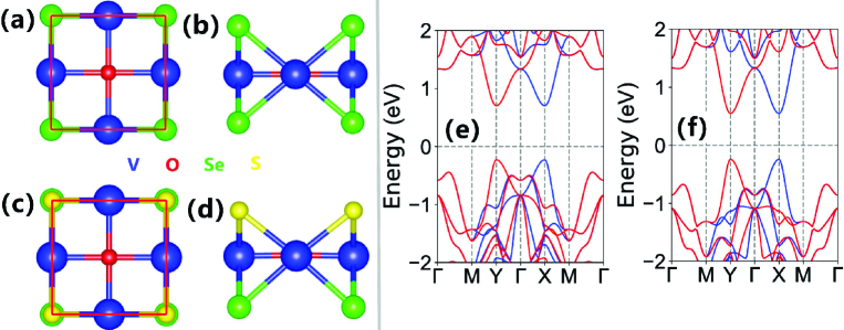
The monolayer has been predicted to be a 2D altermagnetic materialk13 , which possesses three atomic layers with two V atoms and one O atom in the middle layer sandwiched by two Se layers (see Figure 2 (a) and (b)). Each V atom is surrounded by four Se atoms, and the two V atoms in the primitive cell form AFM configuration. The two V atoms have the same surrounding Se atomic arrangement as a rectangle, but the directions of the two rectangle are different ( and directions), which leads to the spin splitting. However, two V-atom related sublattices is related by a diagonal mirror symmetry (see Figure 3), and then two spin channels in the band structures is also related by . It is noted that two V-atom related sublattices cannot be transformed to each other by any translation operation.
Janus monolayer possesses similar crystal structures with (see Figure 2 (c) and (d)), which can be constructed by replacing one of two Se layers with S atoms in monolayer . Each V atom in is surrounded by two S and two Se atoms. The two V atoms have the same surrounding atomic arrangement of S and Se as a rectangle with different orientation. The two V-atom related sublattices is related by . So, the energy band structures between and should be similar.
A Hubbard correction =4.3 eVk13 is used to perform the related calculations, and the optimized lattice constants ==3.88 for . The AFM energy of is 0.582 eV lower than that of FM case. The magnetic moments of two V atoms are 1.833 and -1.838 , and total magnetic moment is strictly 0.00 . The energy band structures of both and are plotted in Figure 2 (e) and (f), and they show the similar energy band structures with obvious spin splitting. It is clearly seen that there are two equivalent valleys at high-symmetry X and Y points for both valence and conduction bands as valence band maximum (VBM) and conduction band bottom (CBM), which are related by . States around X and Y points are mainly from two different V atoms with opposite spins, producing altermagnetism in the absence of SOC. The spin-valley locking can be observed, which can be tuned by uniaxial straink13 . For example, a compressive/tensile strain along direction makes the energies of X and Y valleys be different, producing the spin-valley polarization.
IV 2. monolayer
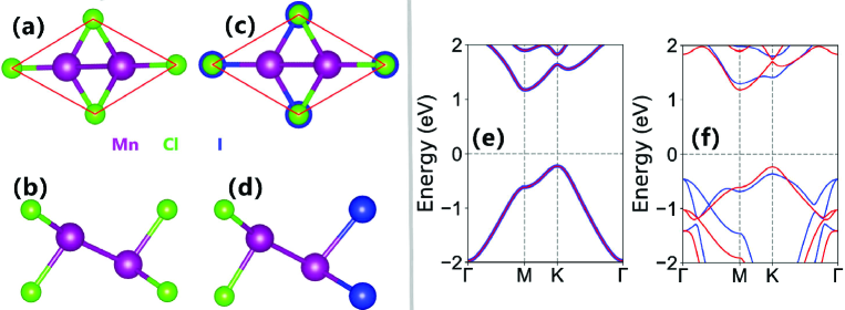
The monolayer is predicted to be a A-type AFM semiconductors without spin splitting, and the spin polarization can be achieved by external electric fieldk15 . is composed of two hexagonal Mn layers sandwiched by two hexagonal Cl layers in the stacking order of Cl-Mn-Mn-Cl with both magnetic atomic layers bonded with metallic bonds and ionic bonds (see Figure 4 (a) and (b)). The two Mn atoms have the same surrounding atomic arrangement of Cl and Mn, which gives rise to the degeneration of electron spin.
Janus monolayer also consists of four atomic layers in the sequence of Cl-Mn-Mn-I (see Figure 4 (c) and (d)), which can be constructed by replacing one of two Cl layers with I atoms in monolayer . The two Mn atoms have the different surrounding atomic arrangement. One Mn atom is sandwiched by Cl and Mn layers, while another Mn atom is sandwiched by I and Mn layers, which can produce spin splitting. Similar to k14 , an intrinsic polar electric field along the direction can be induced due to the different electronegativity of the Cl and I elements, which can realize EPD-AFM.
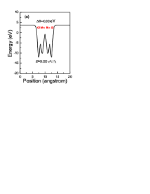
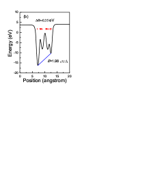
We use a Hubbard correction =4.0 eV to perform the related calculations, and the optimized lattice constants ==3.83 for . The AFM ordering is the ground state, and its energy is 0.535 eV lower than FM energy. The magnetic moments of two Mn atoms are 4.57 and -4.62 with total magnetic moment per unit cell being strictly 0.00 . The energy band structures of both and are shown in Figure 4 (e) and (f). It is clearly seen that no spin splitting can be observed for , while shows obvious spin splitting. This difference is because the possesses the out-of-plane polar electric field, while the built-in electric field of disappears. To clearly identify the inherent electric field of , the planar average of the electrostatic potential energy along direction is plotted in Figure 5 along with that of . The mirror asymmetry can induce an electrostatic potential gradient () of about 0.35 eV for , which is related to the work function change of the structure. The magnitude of the net vertical electric field can be estimated by the slope of the plane-averaged electrostatic potential between top and bottom atoms’ minima. For , the built-in electric field is 0.00 due to out-of-plane structural symmetry, and is 1.98 for with structural asymmetry. So, the possesses EPD-AFM. Calculated results show that is an indirect band gap semiconductor (1.417 eV) with VBM and CBM at high symmetry K and M points, respectively. The VBM and CBM are provided by the same spin-up channel. These results of are similar to those of k14 .
V 3. monolayer
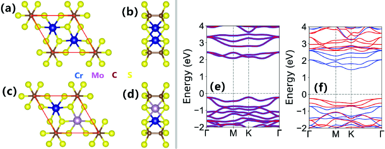
Inspired by the successful synthesis of the 2D monolayer with AFM orderingk17 , we construct the , whose crystal structures are shown in Figure 6 (a) and (b). There are two Cr, two C and six S atoms in the primitive cell. The magnetic Cr atoms form a honeycomb lattice within the same layer. The two Cr atoms in the primitive cell are coordinated by a octahedron of six S atoms from the neighboring ligands 3S-2C-3S with the centers of the hexagons occupied by the C-C units. The two Cr atoms have the same octahedral environment, producing the degeneration of electron spin. To break the equivalence of two magnetic atoms, 2D can be built by substituting one Cr in the via isovalent Mo, which are plotted in Figure 6 (c) and (d). The two magnetic atoms are 3 Cr and 4 Mo, respectively, which have the same surrounding atomic arrangement (see Figure 7). However, the energy level of 4 electron is higher than that of 3 one, which will lead to spin splitting.
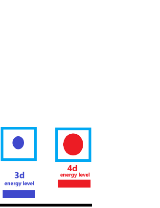
The GGA+ method with a Hubbard =3 eV for both Cr and Mok18 is employed for the related calculations. The optimized lattice constants ==5.714 , which agrees well with previous theoretical valuek18 . The AFM ordering is the ground state with energy difference being -0.580 eV between AFM and FM cases. The magnetic moments of Cr and Mo atoms are 2.88 and -2.34 , respectively. However, the total magnetic moment per unit cell is strictly 0.00 . The energy band structures of both and are shown in Figure 6 (e) and (f). Calculated results show no spin splitting for , and obvious spin splitting for . The spin-down channel from 4 orbital character move toward higher energy than spin-up channel from 3 one. The is a bipolar antiferromagnetic semiconductor with VBM and CBM in different spin channels, and the gap value is 1.702 eV. Compared with and , possesses larger spin splitting and more obvious spontaneous spin polarization. In general, 4 electrons have weaker electron correlation than 3 electrons. A Hubbard correction =3.0/2.0 eV for Cr/Mo is adopted to recalculate the related results. The magnetic ground state is still AFM ordering, and the energy band structures still show obvious spin splitting.
VI 4. monolayer
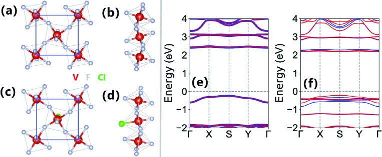
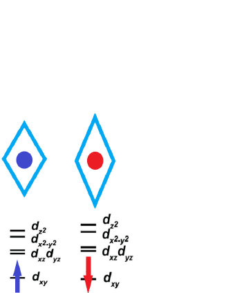
Monolayer is predicted to have antiferromagnetic ferroelasticity and bidirectional negative Poisson’s ratiok19 . The two V atoms are coordinated by a octahedron of six F atoms (see Figure 8 (a) and (b)). According to the following calculation results, the V-F bonds (1.947 ) within the -plane are significantly longer than those (1.747 ) along the -direction, producing Jahn-Teller distortion, which splits the orbitals into four subgroups: the , , and singlets, and the and doublet, with the lowest orbital occupiedk19 . For net in-plane environment, the two V atoms are equivalent, leading to the degeneration of electron spin. To break the equivalence of two magnetic atoms, 2D is constructed by substituting one F in the with Cl (see Figure 8 (c) and (d)). The two V atoms in have different levels of Jahn-Teller distortion, which leads to that the orbitals of two V atoms have different splitting sizes (see Figure 9), producing the spin splitting in the band structures.
The GGA+ method with a Hubbard =3 eV for V atom is adopted for the related calculations. The optimized lattice constants ==5.366 for . The AFM ordering is the ground state, and the energy difference is -0.014 eV between AFM and FM orderings. The magnetic moments of two V atoms are 1.00 and -1.05 , and the total magnetic moment per unit cell is strictly 0.00 . The energy band structures of both and are plotted in Figure 8 (e) and (f). Calculated results show no spin splitting for , and observable spin splitting for . The is an indirect semiconductor (2.416 eV) with VBM (S point) and CBM ( point) in the same spin channels .
VII Discussion and Conclusion
In fact, the four types can coexist with each other in a material. For example a 2D altermagnet, if the magnetic atoms have opposite layer spin polarization (A-type AFM ordering) with an out-of-plane built-in electric field, the spontaneous spin-valley polarization can be producedk14 . The magnetic atoms with opposite layer spin polarization have been predicted in 2D without built-in electric fieldyz . So, it is possible to find electric-potential-difference altermagnet (EPD-AM).
In summary, we propose an intuitional strategy to find or produce spin-splitting in AFM materials without SOC. It is demonstrated that four different types of 2D AFM materials (, , and ) can be used to confirm our proposal. For , the different environment can be induced by the orientation of surrounding atoms arrange. For , the out-of-plane inherent electric field leads to different environment. For , 4 electron has higher energy than 3 electron, which produces different environment. For , different levels of Jahn-Teller distortion gives rise to different environment. To produce spin splitting in AFM materials, other different mechanisms can be found, but the essential reason is that the magnetic atoms with opposite spin polarization locate in the different environment (surrounding atomic arrangement).
Acknowledgements.
Y.S.A. is supported by the Singapore Ministry of Education Academic Research Fund Tier 2 (Award No. MOE-T2EP50221-0019). We are grateful to Shanxi Supercomputing Center of China, and the calculations were performed on TianHe-2.References
- (1) A. Manchon, H. C. Koo, J. Nitta, S. M. Frolov, and R. A. Duine, Nat. Mater. 14, 871 (2015).
- (2) A. Manchon, J. elezn, I. M. Miron, T. Jungwirth, J. Sinova, A. Thiaville, K. Garello, and P. Gambardella, Rev. Mod. Phys. 91, 035004 (2019).
- (3) B. A. Bernevig, J. Orenstein, and S.-C. Zhang, Phys. Rev. Lett. 97, 236601 (2006).
- (4) J. Schliemann, Rev. Mod. Phys. 89, 011001 (2017).
- (5) P. Altmann, M. P. Walser, C. Reichl, W. Wegscheider, and G. Salis, Phys. Rev. B 90, 201306(R) (2014).
- (6) M. I. Katsnelson, V. Yu. Irkhin, L. Chioncel, A. I. Lichtenstein and R. A. de Groot, Rev. Mod. Phys. 80, 315 (2008).
- (7) X. Hu, Adv. Mater. 24, 294 (2012).
- (8) T. Jungwirth, J. Sinova, A. Manchon, X. Marti, J. Wunderlich and C. Felser, Nat. Phys. 14, 200 (2018).
- (9) L. mejkal, J. Sinova and T. Jungwirth, Phys. Rev. X 12, 031042 (2022).
- (10) I. Mazin Phys. Rev. X 12, 040002 (2022).
- (11) L. mejkal, J. Sinova and T. Jungwirth, Phys. Rev. X 12, 040501 (2022).
- (12) L. mejkal, R. Gonzlez-Hernndez, T. Jungwirth and J. Sinova, Sci. Adv. 6, eaaz8809 (2020).
- (13) S. Lpez-Moreno, A. H. Romero, J. Meja-Lpez, A. Muoz and Igor V. Roshchin, Phys. Rev. B 85, 134110 (2012).
- (14) I. I. Mazin, Phys. Rev. B 107, L100418 (2023).
- (15) M. Naka, S. Hayami, H. Kusunose, Y. Yanagi, Y. Motome and H. Seo, Nat. Commun. 10, 4305 (2019).
- (16) L.-D. Yuan, Z. Wang, J.-W. Luo, E. I. Rashba and A. Zunger, Phys. Rev. B 102, 014422 (2020).
- (17) M. Naka, Y. Motome and H. Seo, Phys. Rev. B 103, 125114 (2021).
- (18) X. Chen, D. Wang, L. Y. Li and B. Sanyal, Preprint at https://arxiv.org/abs/2104.07390 (2021).
- (19) P. J. Guo, Z. X. Liu and Z. Y. Lu, npj Comput. Mater. 9, 70 (2023).
- (20) S. D. Guo, X. S. Guo, K. Cheng, K. Wang and Y. S. Ang, Preprint at https://doi.org/10.48550/arXiv.2306.04094 (2023).
- (21) H.-Y. Ma, M. L. Hu, N. N. Li, J. P. Liu, W. Yao, J. F. Jia and J. W. Liu, Nat. Commun. 12, 2846 (2021).
- (22) S. D. Guo, Preprint at https://doi.org/10.48550/arXiv.2307.05010 (2023).
- (23) P. Hohenberg and W. Kohn, Phys. Rev. 136, B864 (1964); W. Kohn and L. J. Sham, Phys. Rev. 140, A1133 (1965).
- (24) G. Kresse, J. Non-Cryst. Solids 193, 222 (1995).
- (25) G. Kresse and J. Furthmller, Comput. Mater. Sci. 6, 15 (1996).
- (26) G. Kresse and D. Joubert, Phys. Rev. B 59, 1758 (1999).
- (27) J. P. Perdew, K. Burke and M. Ernzerhof, Phys. Rev. Lett. 77, 3865 (1996).
- (28) Y. J. Niu, H. F. Lv, X. J. Wu and J. L. Yang, J. Phys. Chem. Lett. 14, 4042 (2023).
- (29) G. Long, H. Henck, M. Gibertini, D. Dumcenco, Z. Wang, T. Taniguchi, K. Watanabe, E. Giannini and A. F. Morpurgo, Nano Lett. 20, 2452 (2020).
- (30) P. Wang, D. X. Wu, K. Zhang and X. J. Wu, J. Phys. Chem. Lett. 13, 3850 (2022).
- (31) L. Zhang, C. Tang and A. J. Du, J. Mater. Chem. C 9, 95 (2021).
- (32) R. W. Zhang, C. X. Cui, R. Z. Li, J. Y. Duan, L. Li, Z. M. Yu and Y. G. Yao, Preprint at https://doi.org/10.48550/arXiv.2306.08902 (2023).