Magneto-optical anisotropies of 2D antiferromagnetic MPX3 from first principles
Abstract
Here we systematically investigate the impact of the spin direction on the electronic and optical properties of transition metal phosphorus trichalcogenides (MPX3, M=Mn, Ni, Fe; X=S, Se) exhibiting various antiferromagnetic arrangement within the 2D limit. Our analysis based on the density functional theory and versatile formalism of Bethe-Salpeter equation reveals larger exciton binding energies for MPS3 (up to 1.1 eV in air) than MPSe3 (up to 0.8 eV in air), exceeding the values of transition metal dichalcogenides (TMDs). For the (Mn,Fe)PX3 we determine the optically active band edge transitions, revealing that they are sensitive to in-plane magnetic order, irrespective of the type of chalcogen atom. We predict the anistropic effective masses and the type of linear polarization as an important fingerprints for sensing the type of magnetic AFM arrangements. Furthermore, we identify the spin-orientation-dependent features such as the valley splitting, the effective mass of holes, and the exciton binding energy. In particular, we demonstrate that for MnPX3 (X=S, Se) a pair of non equivalent K+ and K- points exists yielding the valley splittings that strongly depend on the direction of AFM aligned spins. Notably, for the out-of-plane direction of spins, two distinct peaks are expected to be visible below the absorption onset, whereas one peak should emerge for the in-plane configuration of spins. These spin-dependent features provide an insight into spin flop transitions of 2D materials. Finally, we propose a strategy how the spin valley polarization can be realized in 2D AFM within honeycomb lattice.
I Introduction
The subtle interplay between the spin, charge, orbital, and lattice degrees of freedom driven by the electron correlation is one of the key aspects in condensed matter physics behind novel electronic phases of matter and intriguing physical phenomena. In particular, the electronic properties can be modified whenever the spin direction is altered, as spin-orbit coupling (SOC) depends on the spin direction. For instance, spin-valley coupling serves as the fundamental mechanism in optically-controlled valley polarization Zeng et al. (2012), spin-Hall and valley-Hall effects Xiao et al. (2012). Contrast to most of the findings in non-magnetic 2D materials Tombros et al. (2007); van ’t Erve et al. (2012); Kamalakar et al. (2015), where pseudo-spins are involved, 2D magnets exhibit active carrier spins, enabling studies of magnetism in reduced dimensions Gibertini et al. (2019).
Unlike ferromagnets (FMs), the antiferromagnets (AFMs) are commonly found in nature and they are permitted in each magnetic symmetry group, however they are less utilized than FMs Nemec et al. (2018). Currently, AFM materials are considered as promising candidates for future spintronic applications, due to unique properties including insensitivity to external magnetic fields, lack of stray fields, and ultrafast spin dynamics in the terahertz regime Zhang et al. (2019). The spontaneously long-range ordered of microscopic magnetic moments, resulting in zero net magnetization, which makes the AFMs insensitive to external magnetic fields. Thus, a control of AFM state requires very high magnetic fields and demands unconventional means of detection Nemec et al. (2018).
Many properties such as optical, electronic, and vibrational, rely on the magnetic orderingBirowska et al. (2021); Autieri et al. (2022); Linhart et al. (2023), as well as magnetic moment orientationLiu et al. (2019). In particular, a giant impact of the spin direction on the band structure, have been recently demonstrated for 2D ferromagnetic CrI3 material Jiang et al. (2018). Although, the spin-direction properties are reported for conventional and layered FMs Sander (2004); Grünberg (2001), the research on 2D AFM materials is very limited and scarce Nemec et al. (2018); Gibertini et al. (2019); Martí et al. (2015); Rahman et al. (2021).
One of essential feature for manipulating AFM state is the magnetocrystalline anisotropy (MAE) which is evident in spin flip or spin flop transitions. The latter one requires relatively weak MAE and it is reported in literature for AFM compounds exhibiting various electronic states such as topological insulators Sass et al. (2020), layered materials Balamurugan et al. (2014), and conventional semiconductors Machado et al. (2017). In addition, the experimental techniques including indirect means of magnetic phases such as anisotropic magnetoresistance (AMR), anomalous Hall effect (AHE) or second harmonic generation (SGH)Jungwirth et al. (2016); Nemec et al. (2018); Fina et al. (2014), are employed to detect the AFM orientation in 2D materials. Interestingly, the magnetic phase transition of controlled anisotropic phenomenon in layered magnets provides crucial understanding of fundamental magnetism in reduced dimensions.
The present work is motivated by the lack of systematic studies regarding the impact of AFM orientation of magnetic moments on the optoelectronic properties of 2D materials. Hence, in this paper we put particular attention to pinpoint the magnetic fingerprints in indirect properties that can engineer the AFM ordering. We conduct a theoretical analysis based on density functional theory (DFT) and effective Bethe-Salpeter equation (BSE) to identify various spin direction features, which can be utilised in spin-processing functionalities. This study focuses on spin angle evolution of the effective masses of carriers, optically active band edge transitions, exciton binding energies, which remain almost unexplored in the context of van der Waals (vdW) AFM crystals.
Here, we present a systematic study of the impact of spin orientation on the electronic and optical properties of series of the monolayers of MPX3, where M= Mn, Ni, Fe, and X= S, Se, assuming collinear arrangement of the magnetic moments. The results are presented as following: first we examine the magnetic ground state, determining easy and hard axes of magnetization at the level of PBE+U+SOC approach. Next, we consider the electronic features such as band extrema, effective masses, valley splitting and excitonic properties including the excitonic binding energy. Although, the electronic properties have been widely reported for particular spin arrangement and direction, the impact of the orientation of the collinearly ordered spins on opto-electronic properties MPX3 are largely missing. Finally, band edge excitons have been systematically predicted for this class of materials for the first time.
II Computational Details
The calculations were performed in the framework of density functional theory (DFT) using the generalized gradient approximation within the PBE flavor Paier et al. (2005), as implemented in VASP software Kresse and Furthmüller (1996). The ion–electron interactions were described by the projector augmented wave (PAW) method Holzwarth et al. (2001). Plane-wave basis cutoff and centered Monkhorst-Pack Monkhorst and Pack (1976) k-point grid were set to 500 eV and , respectively. A Gaussian smearing of 0.05 eV was employed for the Brillouin zone (BZ) integration. The interlayer vdW forces were treated within Grimme scheme using D3 correction Grimme et al. (2010). A vacuum of the thickness equal to 20 Å was added to mimic the isolated monolayer. Most of the results were obtained using PBE+U method based on Dudarev’s approach, with the effective on-site Hubbard U parameter (Ueff =U-J, where J=1eV) assumed for orbitals. Note that Ueff is hereafter denoted as U. To check its impact on various properties two values of U= 3, 5 eV were employed. The SOC within the non-collinear treatment of magnetism was taken into account on the top of the PBE+U scheme. The position of the atoms and unit cell were fully optimized within the PBE+U approach. In order to predict the magnetic easy and hard axis, the spins of the magnetic ions have been rotated from out-of plane to in-plane directions with polar angle step =150. For every the atomic positions and the lattice parameters have been fully optimized. The effective masses of carriers at the band edges were examined using finite difference method Fonari and Sutton (2015). The direct interband momentum matrix elements were computed from the wave function derivatives using Density Functional Perturbation Theory (DFPT)Gajdoš et al. (2006) in order to determine the optically active transitions, as discussed in Woźniak et al. (2020). The macroscopic optical dielectric constants frequency were obtained using DFTP in the independent particle approach with (DFT-TD) and without local field effects (IP) Gajdoš et al. (2006)
Exciton calculations were performed within the effective BSE formalismAlbrecht et al. (1998); Rohlfing and Louie (2000); Zollner et al. (2019, 2020, 2023); Birowska et al. (2021) using the effective masses and dielectric constants obtained from the DFT calculations. We solve the effective BSE numerically using the parameters given in Ref.Birowska et al. (2021).
III Results
III.1 Magnetic ground state magnetic easy axis
First, we examine the impact of the rotation of spins on the energy profile to determine the magnetic ground state and magnetic easy/hard axes for all employed MPX3 systems. We assume a collinear alignment of the spins and angle of rotation (see Fig. 1 (a)) varied from the out-of plane to in-plane configuration. The rotation of the spins within the basal plane yields up to two orders of magnitude smaller energy changes compared to out-of plane ones, hence in-plane rotations are not further considered.
The magnetic ground state exhibits antiferromagnetic Neel (AFM-N) and antiferromagnetic zigzag (AFM-z) arrangement of the spins for Mn and M=Ni, Fe, respectively (see Fig. 1), in line with other reports Sivadas et al. (2015); Birowska et al. (2021); Autieri et al. (2022); Budniak et al. (2022). The MPX3 materials are reported to be robust antiferromagnets Autieri et al. (2022) and even high concentration of the substitutional dopants could not alter the magnetic ordering of the host Basnet et al. (2022); Autieri et al. (2022). Additionally, changing the angle of spin alignment requires at least one order of magnitude lower energy (tens of meV per magnetic ion) than change of the AFM ordering (at least tens of meV per magnetic ion). The computed energy difference () between the out-of plane and in-plane directions can be one order of magnitude greater for Se than S compounds (see Fig. 1 (b-d)), which is expected for heavier atoms, exhibiting larger SOC coupling Basnet et al. (2022). Surprisingly, FePS3 exhibits a larger MAE than FePSe3 (see Fig 1(e)). The value of U does affect neither the type of AFM ordering nor the direction of the magnetic easy axis. However, the E depends on the Hubbard U parameters. Namely, the smaller values are generally obtained for larger U, except for FePS3 monolayer (see Fig. S2). For the employed materials, an increase in the effective U resulted in larger lattice constants by up to 1.5 % and larger magnetic moments (see Table S2).
Let us now consider the easy axes of magnetization, which are presented in Fig. 1(f, g) for all employed structures, with the hard axes predicted to be orthogonal to the corresponding easy axis/plane. In particular, for FePX3 the magnetic easy axis points along the crystallographic direction as reported in previous studies Olsen (2021); Wildes et al. (2015); Kurosawa et al. (1983); Koo et al. (2021); Sivadas et al. (2015, 2015); Wiedenmann et al. (1981). Hence, this kind of systems are considered to be Ising-type antiferromagnets, with a strong uniaxial magnetic anisotropy.
For the MnPX3 compounds, we predict that the easy plane coincides with monolayer plane, unlike the recent experimental report for MnPS3, which has demonstrated that the spins are slightly tilted from the -axis Ressouche et al. (2010). The direction of the ordered spins for MPX3 compounds result from the interplay between the single-ion anisotropy and magnetic dipolar interactions (MDIs), as already discussed in a recent publication Basnet et al. (2022). In addition, the spin-orbit splitting is negligible for MnPS3, which manifests itself as the lowest MAE for all employed structures (see Fig. 1(b,e)). Thus, the MDI, generally regarded to be weakJohnston (2016), might be decisive in determining the direction of the MnPS3 spins. Note, that the MDIs are not accounted for in our PBE+U+SOC approach, and will be considered elsewhere. On the other hand, in the case of the MnPSe3, the MDIs could be neglected due to larger lattice parameters and SOC. Hence, the magnetic easy axis of MnPSe3 coincides with the monolayer plane, in agreement with other reports in the literatureSen and Chouhan (2020); Wiedenmann et al. (1981); Kurosawa et al. (1983), and confirmed by spin flop transition reported upon the nonmagnetic substitution in MnPS3 thin films Basnet et al. (2022). Regarding NiPS3, the in-plane position of the magnetic moments are preferable and the magnetic ordering can be described by the XY Heisenberg HamiltonianWildes et al. (2015); Olsen (2021); Hwangbo et al. (2021); Belvin et al. (2021). Our results predict the easy axis of magnetization within the monolayer frame, without any deviation in the z direction as reported recently for monolayerKim et al. (2019). However, we do not exclude the possibility that the inclusion of the MDIs interaction can facilitate the rotation of the spins towards the out of the plane direction. For the case of NiPSe3, we determined the easy axis of magnetization to be in out-of-plane direction in line with recent report Sun et al. (2023). Similar results regarding the easy axis/plane of magnetization have been reported for the corresponding bulk systems Basnet et al. (2022).
| MPX3 (magn. state) | spin direction () | K+/K- (, ) | Spin Deg. (, ) | Hex. symm. | (pol.) Inten. [] |
|---|---|---|---|---|---|
| MnPS3 (AFM-N)) | 00 | (-6.4, -4.4) | X | (z) 0.59 | |
| 900 | X (0, 0) | X | (z) 0.62 | ||
| MnPSe3 (AFM-N) | 00 | (-17.7, 33.1) | X | (z) 0.13 | |
| 900 | X (0, 0) | X | (z) 0.18; (x,y) 0.05 | ||
| FePS3 (AFM-z) | 00 | X | (1.8, 9.1) | broken | 0.71 (y) |
| 900 | X | (1.5, 7.4) | broken | 0.73 (y) | |
| FePSe3 (AFM-z) | 00 | X | (7.4, 3.1) | broken | (y) 0.27; (x) 0.04 |
| 900 | X | (9.3, 5) | broken | (y) 0.29; (x) 0.02 |
III.2 Electronic properties
electronic band gaps
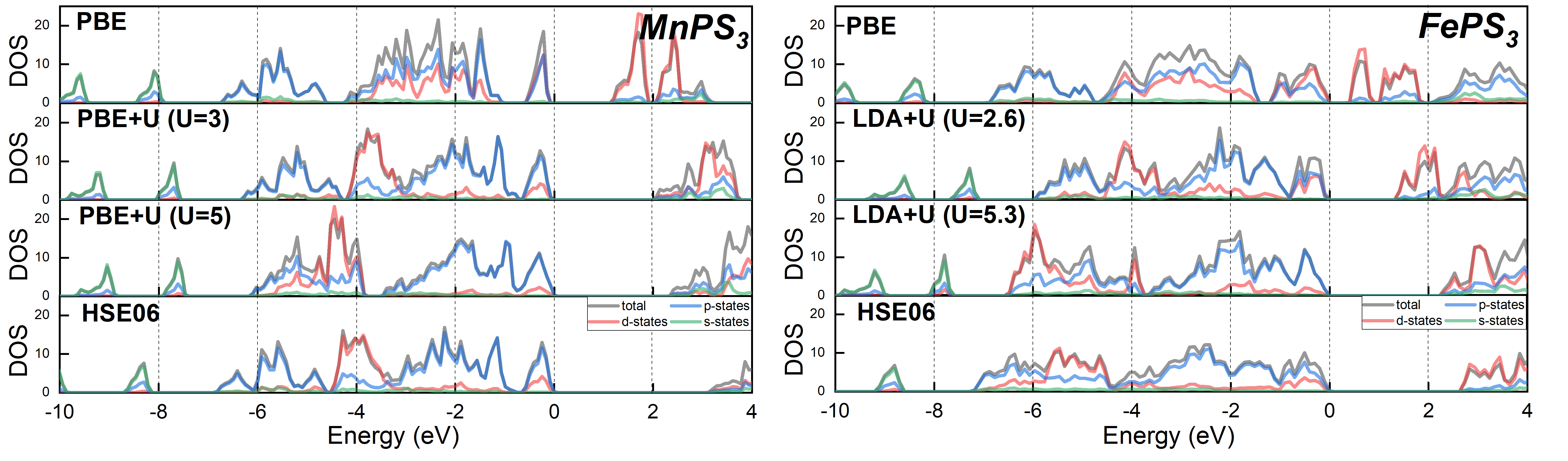
Our results reveal that the structures containing Mn and Fe exhibit direct band gaps located at K high symmetry point (see Fig. 2 (a)), in line with previous reports Birowska et al. (2021); Budniak et al. (2022); Geraffy et al. (2022), while the NiPS3 system is an indirect semiconductor confirmed by experiments Hwangbo et al. (2021). In particular, for FePS3 and NiPSe3 there is a strong contribution of the states to the bands in vicinity of Fermi level. Hence, for these systems, significant changes of the position of the band extrema (VBM, CBM) and their curvatures upon the Hubbard U parameter are visible (see Tables S2 and S3 and discussions therein).
U dependence
For all employed compounds, except MnPX3, the U parameter significantly affects the curvature of the conduction bands as reported previously Budniak et al. (2022), and hence the effective masses of holes. Hence, all features are examined assuming two Hubbard U parameters U=3, 5 eV). In particular, the large value of the effective masses of electrons exhibited for Ni contained systems, indicating a flat character of the conduction bands, which can be further enhanced by adopting larger values of U (see Table S3). By applying the Hubbard U to 3d states, one can shift the 3d states away from the Fermi level. In particular, for MnPX3 structures the conduction bands are mainly build from p-states, and further shifting 3d states do no affect the band curvature nor the band gap value, whereas for FePX3 compounds the conduction bands consist mainly of 3d states, hence further enlargement of U strongly impacts electronic features around band edges. Additionally, our results corroborate the previous reports on strong dependence of Hubbard U on fundamental energy band gap (see Table S2) Budniak et al. (2022).
Effective masses
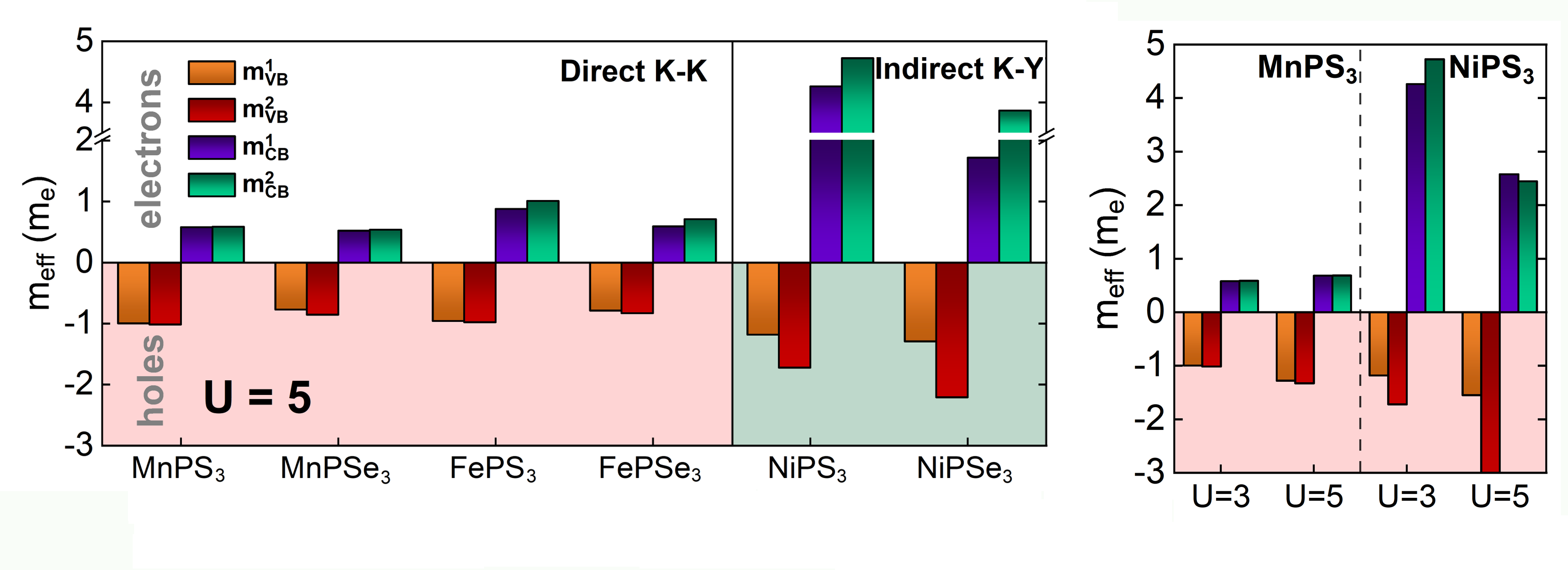
For all of employed monolayers, the heaviest effective mass is obtained for NiPX3, whereas the lightest one is demonstrated for MnPSe3 (see Table S3 and Fig. S3). Generally, the lower effective masses are exhibited by the electrons than holes, and for Se contained structures than corresponding S systems (by about 30), except for NiPX3 structures where these trends are opposite. Additionally, the anisotropic in-plane components of effective masses (m m2) are exhibited by monolayer with AFM-z ground state, whereas for MnPX3 monolayers with AFM-N ordering, the in-plane components are isotropic (m1=m2). Note, that the AFM-z magnetic arrangement breaks the hexagonal symmetry, as it consist of spins ferromagnetically aligned along zigzag chain (see Fig 1(g)), whereas the AFM-N type of magnetic order is commensurate with the structural symmetry. Hence, the anisotropic effective masses, and thus, anisotropic transport properties can be regarded as a magnetic marker distinguishing different type of antiferromagnetic ordering within hexagonal lattice. In addition, the inclusion of the SOC does not affect the curvature of examined systems, except for MnPSe3 where slight changes are shown for K+ and K- valleys (see Table S4).
Spin-orientation-dependent electronic features in MPX3 (M=Mn, Fe; X=S,Se)
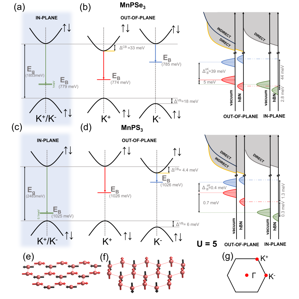
Now, let us make closer inspection on the band edges of MLs exhibiting direct transitions. The electronic features are collected in Table S3. Note, that in the absence of the SOC, the band extrema are doubly degenerated for all employed systems. The presence of SOC in the structures containing Mn preserves the spin degeneracy of the band extrema (VBM, CBM), however causing the valley splitting at +K and -K, which is expected for the honeycomb lattice with AFM-N arrangements of the spins with SOC includedLi et al. (2013). Namely, the SOC preserves the spin degeneracy but leads to a renormalization of the valleys (+K and -K are not equivalent) for AFM-N magnetic ground state. The size of the valley splitting () depend on the chalcogen atoms (larger values for Se atoms), Hubbard U, and spin directions (see Fig. 2 and Tables 1, S6). In particular, the largest valley splitting is attained for the out-of-plane direction of the spins ( meV for MnPSe3 and U=3eV) and lower value of U as presented in Fig. 2(c), whereas no polarity of the valleys are observed for the in-plane direction of the spins. Namely, the rotation of the spins towards out-of-plane directions results in enhancement of the valley splitting. Hence, the band gap of MnPSe3 can be changed by up to 35 meV as presented in Fig. 2(b, c), whereas for the rest of the compounds the minor changes are observed (see Fig. 2(b)). Additionally, the effective masses of holes for MnPSe3 are sensitive to the direction of the spins as presented in Fig. 2(d). Interestingly, in the case of MnPS3, the band gap changes its character from direct to indirect when the spins are rotated from an out-of-plane to an in-plane directions.

Regarding the monolayer of FePX3, the presence of SOC and local inversion symmetry breaking in FeX6 octahedra lift the degeneracy of the band extrema (few meV), irrespective to the spin direction (see column 4 in Table 1). In particular, larger spin polarization is obtained for CBM than VBM (= 9.1 meV, = 1.8 meV), and for higher values of U for FePS3. In contrast to the FePS3, the opposite trends are obtained for FePSe3 (for the details see Table S6). Hence, the spin splitting of the bands is obtained for hexagonal lattices exhibiting in-plane structural anisotropy, as reported for MnPS3 (see Fig. 5(d) in Geraffy et al. (2022)). In this case the spin polarization occurred, alongside with renormalization of the +K/-K valleys as expected for AFM-N. In addition, one of the consequences of the local inversion symmetry breaking exploited in Fe monolayers is a lattice distortion reflected in the ratio of the lattice parameters deviated from hexagonal symmetry () Geraffy et al. (2022); Ghosh et al. (2023).
III.3 Excitonic properties
Dielectric properties
We start our discussion by analyzing the dielectric properties of the employed systems. Generally, the in-plane components of static dielectric constants (, ) are isotropic for all studied systems, except for monolayers of (Ni,Fe)PX3, where they differ by up to 4 (see SI and Tabs. S7, S8). Due to the fact that dielectric tensor is well defined for the bulk materials, we calculate the 2D polarizability (dielectric screening length, for the details see SM). Our results reveal that the dielectric screening length increases as the atomic number of the metal also increases , exhibiting the smallest and highest values equal to 3.25 Å (MnPSe3, U=5 eV) and 6.13 Å (NiPSe3, U=5eV), respectively. In addition, the systems containing Se exhibit 40 larger screening properties than their corresponding S systems. The screening properties of MPX3 compounds are generally smaller than for other vdW structures such as MoSe2 (8.23 Å). Note that for the (Ni,Fe)PX3 systems, the dielectric screening lengths strongly depend on the Hubbard U. In particular, the larger values of are attained for the smaller Hubbard U, which correlates with the strong impact of the U on the DOS (see Fig. S2 (b)).
Band edge excitons
Let us now examine the band edge excitons using the relevant information from DFT (, ) combined with the effective BSEAlbrecht et al. (1998); Rohlfing and Louie (2000). We show the exciton binding energies (EB) in Fig. 3(a) (for the details of calculations see Ref.Birowska et al. (2021)). All employed structures exhibit large EB exceeding 1 eV and 0.8 eV for bare monolayers of MPS3 and MPSe3, respectively, outperforming the values in TMDCs Birowska et al. (2021) (the exact values are collected in Tables S9, S10). The excitons have been recently experimentally reported for few layers of NiPS3 Kang et al. (2020); Hwangbo et al. (2021); Wang et al. (2021), and FePS3 Geraffy et al. (2022), however, their origin is still under a hot debate. Generally the EB are larger by about 30 for S contained structures than corresponding Se compounds, mainly due to larger effective masses and smaller dielectric screening for MPS3. The EB decreases as the effective dielectric constant of the environment increases, preserving the same trend for all monolayers. This can be explained within the oversimplified exciton picture (hydrogen model) for which EB is proportional to effective mass and inversely proportional to the square of dielectric screening.
Optical transitions and selection rules
Besides the binding energy, it is also relevant to determine the selection rules of the direct band edge transitions, which are summarized in Table S3. All of the transition are optically allowed (non-zero oscillator strength) exhibiting linear polarization of light. In particular, for monolayers with AFM-N phase (MnPX3) the polarization of light is along direction, whereas for the AFM-z (FePX3) pointing along direction. Interestingly, similar conclusions are observed assuming various AFM metastable phases within the same magnetic material Birowska et al. (2021). Therefore, the polarization of light is sensitive to magnetic order irrespective of the type of transition metal and chalcogen atoms. This is in line with recently reported linear polarization of the sharp emission, that aligned perpendicular to the spin orientation Wang et al. (2021). Hence, the polarization of light might be a tool to distinguish the type of AFM ordering. All of these direct band edge excitons are optically active transitions and couple to -polarized light. Comparing with the widely studied TMDCs, these transitions in MPX3 systems have an intensity two orders of magnitude smaller than the bright (A and B) transitions but have comparable intensity to the dark (D) transitionsWoźniak et al. (2020); Faria Junior et al. (2022).
Spin-orientation-dependent excitonic features in MnPX3
Interestingly, the excitonic properties are sensitive to the direction of the spins. Owing to the spin direction dependent effective masses observed in MnPX3 presented in Fig. 2 (d), we discuss below only these type of monolayers. The effect of the spin direction on EB is on the order of 1-2 meV in MnPS3 but on the order of 10 meV in MnPSe3 monolayer, as presented in Fig. 3 (b), irrespective of the value used for the Hubbard U parameter. Furthermore, opposite K-valleys (at K and K) show different effective masses and, consequently, different values of EB, as shown in Fig. 3(c). Hence, the EB depends on the orientation of the AFM aligned spins. Particularly, due to the sizeable valley-dependent curvature of the VBM (see Fig. 2 (d)) observed for the MnPSe3, the EB of excitons at valleys differ by up to E E = 12 meV (for MnPSe3 in vacuum).
Combining the information of the optical selection rules and exciton binding energies, we present in Fig.S8 the schematic diagram of optically active band edge transition considering the in-plane and out-of the plane direction of spins. Our calculations reveal that the emissions from the opposite and valleys are energetically below the onset of absorption spectrum. For the in-plane directions of the spins, the energy difference between and is rather small (separated about 1 meV and 0.1 meV for MnPSe3 and MnPS3, respectively, as shown in Figs. S8(a,d)). On the other hand, for out-of-plane spins, the exciton emission from K valleys are separated by 42 meV and 6 meV for MnPSe3 and MnPS3, respectively. The separation of the exciton peaks at valleys (see difference between the position of the B and C peaks in Fig. S8) is calculated as:
| (1) |
where is the difference between the exciton binding energies at valleys and the electronic band gap at a given valley. We predict that one peak should be observed for in-plane oriented spins (green peak in Fig. S8) whereas two peaks emerge for the spins deflected from the monolayer plane (red and blue peaks in Fig. S8). Therefore, the energy is a robust magnetic fingerprint of the AFM spin directions. Note that the energy separation of K valleys depends on the dielectric environment, as presented in Fig. 3(c), but should be visible in hBN encapsulated samples, specially in MnPSe3 since the valley splitting is dominated by the electronic counterparts and .
IV Conclusions
Here, we systematically examine the MPX3 materials emphasizing the role of spin reorientation, magnetic arrangement and electron correlation effects in various properties. In this regard, the chemical trends in respect to the type of the chalcongen atom as well as transition metal are examined. We have demonstrated that the electronic features such as band gaps, effective masses, dielectric screening and exciton binding energies strongly depends on the type of chalcogen atom. Notably, larger effective masses are attained for S than Se contained monolayers (by about 30 ), whereas smaller dielectric screening (up to ) are reached for MPS3. In general, the larger effective masses and smaller dielectric screening length are obtained for employed materials than for widely examined TMDs, resulting in larger exciton binding energies of direct transitions of MPX3 than corresponding monolayers of TMDcs. Generally, all examined band edge direct transitions of (Mn,Fe)PX3 monolayers turned out to be optically active coupled to linear polarized light, with type of polarization sensitive to magnetic arrangement.
Regarding the direct band edge transitions, the MnPX3 are of particular importance as could be exploited as promising valley electronics materials. In particular, we have shown that the valley splitting at the can be effectively controlled by the direction of the magnetic moments. In particular, the sizable valley splitting occurs for the out-of plane direction of the magnetic moments in monolayer of MnPSe3 (smaller effect observed for MnPS3), resulting in valley dependent gaps. Namely, two distinct peaks are expected to be visible below the absorption onset for the out-of-plane AFM aligned spins, whereas one peak for the in-plane case. Hence, the number of the peaks and the separation of the peaks can be regarded as magnetic fingerprint of the orientation of AFM aligned spins. The change in the separation of the peaks points towards the plausible spin rotation.
On the other hand, the valleys obtained for MnPX3 are spin degenerated, which might hinder their spintronic applications. Hence, we have also propose a novel way how the spin valley polarization can be attained. We have suggested that particular deformation of the hexagonal lattice of MnPX3 could lead to the spin resolved valley splitting. Our results give insight into the valley splitting realization in 2D antiferromagnets. In addition, the anistropic effective masses and the type of linear polarization can be regarded as magnetic markers probing the type of AFM arrangements. Finally, the spin dependent features have been identified such as valley splitting of VBM and CBM, the effective mass of holes and exciton binding energies. These features can be referred as sensitive parameters that provide insight into spin flop transitions.
V Acknowledgment
M.B. acknowledges financial support from the University of Warsaw under the "Excellence Initiative - Research University" project. P.E.F.J. and J.F. acknowledge the financial support of the Deutsche Forschungsgemeinschaft (DFG, German Research Foundation) SFB 1277 (Project-ID 314695032, projects B07 and B11), SPP 2244 (Project No. 443416183), and of the European Union Horizon 2020 Research and Innovation Program under Contract No. 881603 (Graphene Flagship). T.W. acknowledges financial support of National Science Centre, Poland under grant no. 2021/41/N/ST3/04516. Access to computing facilities of the Interdisciplinary Center of Modeling (ICM), University of Warsaw are gratefully acknowledged. We gratefully acknowledge the Polish high-performance computing infrastructure PLGrid (HPC Centers: ACK Cyfronet AGH) for providing computer facilities and support within computational grants no. PLG/2022/015685 and PLG/2023/016571. We acknowledge ACK Cyfronet AGH (Poland) for awarding this project access to the LUMI supercomputer, owned by the EuroHPC Joint Undertaking, hosted by CSC (Finland) and the LUMI consortium through Pl-Grid organization (Poland), under the grant entitled: "Electronic, optical and thermoelectric properties of selected layered materials and selected heterostructures".
Supplementary Material:
"Magneto-optical anisotropies of 2D antiferromagnetic MPX3 from first principles"
Miłosz Rybak,3 Paulo E. Faria Junior,2 Tomasz Woźniak,3 Paweł Scharoch,3 Jaroslav Fabian,2 and Magdalena Birowska1,∗
1University of Warsaw, Faculty of Physics, 00-092 Warsaw, Pasteura 5, Poland
2Institute for Theoretical Physics, University of Regensburg, 93040 Regensburg, Germany
3Department of Semiconductor Materials Engineering Faculty of Fundamental Problems of Technology Wrocław University of Science and Technology Wybrzeże Wyspiańskiego 27, 50-370 Wrocław, Poland
∗Electronic address: Magdalena.Birowska@fuw.edu.pl
Magdalena Birowska
Determination of Hubbard U from Ab initio
To estimate the Hubbard parameter, we adopt the linear response method proposed by method of Anisimov and co-workers in the framework of a plane-wave pseudopotential approach implemented in VASP by Cococcioni et. al Cococcioni and de Gironcoli (2005). The U parameter is found from the linear fits for both non-selfconsistent (NSCF) as and selfconsistent (SCF) response functions as defined . The results of U parameters for d electrons of transition metal ions are collected in Table S2.
| 4.9 | 5.3 | 5.1 | 5.6 | 5.6 | 5.6 | 5.7 |
Tables of collected electronic features.
| ML of MPX3 | Ueff [eV] | magn. state | lattice constant [Å] | [] | Band gap [eV] | VBM CBM |
|---|---|---|---|---|---|---|
| MnPS3 | 5 | AFM-N | 6.108 | 4.610 | 2.502 (D) | K |
| 3 | AFM-N | 6.098 | 4.491 | 2.242 (D) | K | |
| MnPSe3 | 5 | AFM-N | 6.424 | 4.606 | 1.846 (D) | K |
| 3 | AFM-N | 6.385 | 4.475 | 1.662 | K | |
| NiPS3 | 6.45 | AFM-zig | 5.856 | 1.621 | 2.288 | KY |
| 5 | AFM-zig | 5.839 | 1.522 | 1.954 | KY | |
| 3 | AFM-zig | 5.819 | 1.378 | 1.572 | KY | |
| NiPSe3 | 6.45 | AFM-zig | 6.184 | 1.566 | 1.883(D) | K |
| 5 | AFM-zig | 6.168 | 1.457 | 1.6564 | KY | |
| 3 | AFM-zig | 6.146 | 1.291 | 1.258 | (0.282;0.5;0)Y | |
| FePS3 | 5.3 | AFM-zig | 5.988 | 3.704 | 2.423(D) | K |
| 2.6 | AFM-zig | 5.963 | 3.422 | 1.736 | (0.273;0;0) | |
| FePSe3 | 5.3 | AFM-zig | 6.304 | 3.687 | 1.825(D) | K |
| 3 | AFM-zig | 6.274 | 3.527 | 1.482(D) | K |
| ML of MPX3 | U [eV] | eff. mass of holes m1 [princ. axis], m2 [princ. axis] | eff. mass of electrons m1 [princ. axis], m2 [princ. axis] |
|---|---|---|---|
| MnPS3 | 5 | -0.957 [0.97 0.23 0] -0.955 [-0.23 0.97 0] | 0.577 [-0.39 0.93 -0.1] 0.588 [0.93 0.39 0.1] |
| 3 | -1.244 [0.97 -0.23 0] -1.246 [0.23 0.97 0] | 0.691 [0.99 -0.13 0] 0.689 [0.13 0.99 0] | |
| MnPSe3 | 5 | -0.767 [-0.39 0.93 0] -0.768 [0.93 0.39 0] | 0.546 [0.93 -0.39 0] 0.546 [0.93 0.39 0] |
| 3 | -1.023 [0.97 -0.23 0] -1.026 [0.23 0.97 0] | 0.625 [ 0.95 -0.32 0] 0.623 [0.32 0.95 0] | |
| NiPS3 | 5 | -1.183 [0 1 0] -1.722 [1 0 0] | 4.724 [0 1 0] 4.262 [1 0 -0.01] |
| 3 | -1.550 [0 1 0] -16.592 [1 0 -0.1] | 2.577 [1 0 -0.1] 2.447 [0 1 0] | |
| NiPSe3 | 5 | -1.293 [0 1 0] -2.209 [1 0 0] | 3.865 [0.1 1 0] 1.718 [1.0 -0.1 -0.1] |
| 3 | -1.380 [1 0 0] -4.628 [0 1 -0.1] | 1.869 [0.1 1 0] 1.031 [1 -0.1 -0.1] | |
| FePS3 | 5.3 | -0.927 [0 1 0.1] -0.969 [1 0 0] | 1.053 [0.1 1 0] 0.938 [1 -0.1 0] |
| FePSe3 | 5.3 | -0.772 [0 1 -0.1] -0.788 [1 0 0] | 0.578 [-0.39 0.93 -0.1] 0.577 [0.93 0.39 0.1] |
| 3 | -1.056 [-0.01 1 0] -1.334 [1 0.01 -0.01] | 1.087 [0.04 1 0] 1.045 [1 -0.04 0] |
| method | band edge | k-point | holes: m1 [principle axis] | m2 [principle axis] | SO offset [meV] | ||||||
|---|---|---|---|---|---|---|---|---|---|---|---|
| without SO | VB | K/K’ | -0.767 | [-0.38 | 0.92 | 0.00] | -0.768 | [0.92 | 0.38 | 0.00] | - |
| with SOC: in-plane spins | VB | K | -0.752 | [0.52 | 0.86 | 0.00] | -0.825 | [0.86 | -0.52 | 0.00] | 0 |
| VB | K’ | -0.767 | [0.74 | -0.67 | 0.00 ] | -0.807 | [0.67 | 0.74 | 0.00] | 0 | |
| with SOC: out-of-plane | VB | K | -0.752 | [0.52 | 0.86 | 0.00] | -0.825 | [0.86 | -0.52 | 0.00] | -17.9 |
| VB | K’ | -0.767 | [0.74 | -0.67 | 0.00] | -0.807 | [0.67 | 0.74 | 0.00] | 0.21 | |
| method | band edge | k-point | electrons: m1 [principle axis] | m2 [principle axis] | SO offset [meV] | ||||||
| without SO | CB | K/K’ | 0.547 | [0.92 | -0.38 | 0.00] | 0.546 | [0.38 | 0.92 | 0.00] | - |
| with SOC: in-plane spins | CB | K | 0.551 | [0.83 | -0.56 | 0.00] | 0.542 | [0.56 | 0.83 | 0.00] | -6.39 |
| CB | K’ | 0.551 | [0.59 | 0.81 | 0.00] | 0.541 | [0.81 | -0.59 | 0.00] | -6.39 | |
| with SOC: out-of-plane spins | CB | K | 0.551 | [0.83 | -0.56 | 0.00] | 0.542 | [0.56 | 0.83 | 0.00] | -3.50 |
| CB | K’ | 0.551 | [0.59 | 0.81 | 0.00] | 0.541 | [0.81 | -0.59 | 0.00] | -36.60 | |
| U [eV] | MAE | [meV] | [meV] | [meV] | [meV] | [meV] | [meV] | |
| MnPS3 | 3 | 0.041 | 0 | 0 | 5.5 | 9.3 | 2.203 | 2.194 |
| 5 | 0.028 | 0 | 0 | 6.5 | 3.9 | 2.483 | 2.479 | |
| 7 | - | 0 | 0 | 6.9 | 1.9 | 2.667 | 2.665 | |
| MnPSe3 | 3 | 0.315 | 0 | 34.4 | 17.8 | 0 | 1.689 | 1.654 |
| 5 | 0.223 | 0 | 27.9 | 15.4 | 0 | 1.853 | 1.825 | |
| 7 | - | 0 | 16.4 | 12.6 | 0 | 1.960 | 1.944 |
| valley splitting | MnPSe3 | for U=3eV | MnPSe3 | for U=5eV | MnPS3 | for U=3eV | MnPS3 | for U=5eV |
|---|---|---|---|---|---|---|---|---|
| in-plane spins | -5.7 | 0 | 0 | 0 | 0 | 0 | 0 | 0 |
| out-of-plane spins | -21.5 | 38.6 | -17.7 | 33.1 | -6.6 | -10.3 | -6.4 | -4.4 |
| Spin degeneracy of the band edges | FePS3 | for U=2.6eV | FePS3 | for U=5.3eV | FePSe3 | for U=3eV | FePSe3 | for U=5.3eV |
| in-plane spins | 0 | 7.5 | 1.8 | 9.1 | 7.4 | 5.5 | 7.4 | 3.1 |
| out-of-plane spins | 0 | 6.4 | 1.5 | 7.4 | 11.5 | 8.2 | 9.3 | 5 |
| Magn. | U [eV] | method | , | [Å] |
|---|---|---|---|---|
| MnPS3 | 5 | IP | 2.35 2.35 | 3.25 3.25 |
| 5 | TD-DFT | 2.16 2.16 | 2.80 2.80 | |
| MnPSe3 | 5 | IP | 2.60 2.60 | 4.50 4.50 |
| 5 | TD-DFT | 2.42 2.42 | 3.99 3.99 | |
| NiPS3 | 5 | IP | 2.84 2.82 | 4.28 4.23 |
| 5 | TD-DFT | 2.70 2.68 | 3.94 3.90 | |
| NiPSe3 | 5 | IP | 3.31 3.26 | 6.13 6.00 |
| 5 | TD-DFT | 3.18 3.13 | 5.76 5.65 | |
| FePS3 | 5.3 | IP | 3.20 3.21 | 3.51 3.52 |
| 5.3 | TD-DFT | 2.96 2.95 | 3.13 3.10 | |
| FePSe3 | 5.3 | IP | 2.81 2.78 | 4.90 4.84 |
| 5.3 | TD-DFT | 2.63 2.61 | 4.43 4.38 |
| Magn. | U [eV] | method | , | [Å] |
|---|---|---|---|---|
| MnPS3 | 3 | IP | 2.44 2.44 | 3.45 3.45 |
| 3 | TD-DFT | 2.26 2.26 | 3.02 3.02 | |
| MnPSe3 | 3 | IP | 3.02 3.02 | 4.82 4.82 |
| 3 | TD-DFT | 2.82 2.82 | 4.33 4.33 | |
| NiPS3 | 3 | IP | 3.15 3.10 | 5.12 5.01 |
| 3 | TD-DFT | 3.02 2.98 | 4.82 4.72 | |
| NiPSe3 | 3 | IP | 4.14 4.02 | 7.51 7.21 |
| 3 | TD-DFT | 3.02 2.98 | 4.82 4.72 | |
| FePSe3 | 3 | IP | 3.06 3.03 | 5.56 5.49 |
| 3 | TD-DFT | 2.91 2.89 | 5.15 5.09 |
| system | U [eV] | spin direction [0] | E in vacuum | E in hBN | E in vacuum | E in hBN |
|---|---|---|---|---|---|---|
| MnPS3 | U=3 | 0 | 1032.19 | 344.46 | 1034.46 | 346.02 |
| 50 | 1032.47 | 344.67 | 1034.39 | 345.83 | ||
| 90 | 1033.37 | 345.34 | 1033.48 | 345.45 | ||
| U=5 | 0 | 1023.98 | 322.49 | 1025.60 | 323.21 | |
| 50 | 1023.98 | 322.49 | 1025.60 | 323.21 | ||
| 90 | 1024.69 | 322.79 | 1024.54 | 322.85 | ||
| MnPSe3 | U=3 | 0 | 770.25 | 266.92 | 787.82 | 278.42 |
| 50 | 773.76 | 269.31 | 785.75 | 276.89 | ||
| 90 | 780.62 | 273.32 | 779.96 | 273.13 | ||
| U=5 | 0 | 773.71 | 254.23 | 785.49 | 261.16 | |
| 50 | 775.00 | 254.61 | 781.97 | 259.01 | ||
| 90 | 778.86 | 256.97 | 779.77 | 257.45 |
| ML | U=3 eV, IP | U=3 eV, TD-DFT | U=5 eV, IP | U=5 eV, TD-DFT | |
|---|---|---|---|---|---|
| 1.0 | 1028.58 | 1132.13 | 1019.06 | 1132.42 | |
| 1.5 | 814.46 | 890.75 | 797.34 | 879.03 | |
| 2.0 | 673.53 | 732.35 | 652.41 | 714.90 | |
| 2.5 | 571.60 | 618.59 | 549.11 | 598.30 | |
| MnPS3 | 3.0 | 494.27 | 532.73 | 470.56 | 510.31 |
| 3.5 | 433.05 | 464.87 | 409.35 | 442.17 | |
| 4.0 | 383.39 | 410.52 | 360.20 | 387.07 | |
| 4.5 | 342.54 | 365.24 | 319.61 | 342.01 | |
| 5.0 | 308.07 | 327.64 | 285.84 | 304.97 | |
| 1.0 | 778.82 | 843.61 | 778.93 | 850.94 | |
| 1.5 | 623.37 | 671.57 | 616.20 | 668.73 | |
| 2.0 | 519.65 | 557.50 | 508.78 | 549.51 | |
| 2.5 | 444.61 | 475.08 | 431.41 | 463.95 | |
| MnPSe3 | 3.0 | 386.72 | 412.18 | 372.29 | 398.80 |
| 3.5 | 340.69 | 362.07 | 325.94 | 347.92 | |
| 4.0 | 303.63 | 321.54 | 288.12 | 306.50 | |
| 4.5 | 272.23 | 287.72 | 256.96 | 272.58 | |
| 5.0 | 246.07 | 259.44 | 230.95 | 244.25 | |
| 1.0 | 985.67 | 1031.65 | 1073.15 | 1140.95 | |
| 1.5 | 825.85 | 862.46 | 886.32 | 939.24 | |
| 2.0 | 716.31 | 746.68 | 759.50 | 802.73 | |
| 2.5 | 634.46 | 660.29 | 665.62 | 701.86 | |
| NiPS3 | 3.0 | 569.94 | 592.46 | 592.25 | 623.30 |
| 3.5 | 517.45 | 537.29 | 532.90 | 559.77 | |
| 4.0 | 473.66 | 491.15 | 483.65 | 507.35 | |
| 4.5 | 436.31 | 451.94 | 442.10 | 462.95 | |
| 5.0 | 404.01 | 418.21 | 406.42 | 424.93 | |
| 1.0 | 670.36 | 940.83 | 805.38 | 844.93 | |
| 1.5 | 562.14 | 775.12 | 673.12 | 704.36 | |
| 2.0 | 487.23 | 662.72 | 582.05 | 608.00 | |
| 2.5 | 430.83 | 579.42 | 513.95 | 536.08 | |
| NiPSe3 | 3.0 | 386.65 | 514.41 | 460.50 | 479.60 |
| 3.5 | 350.42 | 462.08 | 416.84 | 433.64 | |
| 4.0 | 320.06 | 418.51 | 380.60 | 395.41 | |
| 4.5 | 294.47 | 381.96 | 349.65 | 362.93 | |
| 5.0 | 272.19 | 350.44 | 323.07 | 334.86 | |
| 1.0 | 1038.18 | 1132.84 | - | - | |
| 1.5 | 825.91 | 896.20 | - | - | |
| 2.0 | 685.68 | 740.31 | - | - | |
| 2.5 | 584.24 | 628.15 | - | - | |
| FePS3 | 3.0 | 506.71 | 543.07 | - | - |
| 3.5 | 445.41 | 475.55 | - | - | |
| 4.0 | 395.42 | 420.84 | - | - | |
| 4.5 | 354.01 | 375.72 | - | - | |
| 5.0 | 319.04 | 338.00 | - | - | |
| 1.0 | 766.45 | 812.40 | 741.87 | 798.61 | |
| 1.5 | 626.08 | 661.47 | 590.19 | 632.78 | |
| 2.0 | 530.94 | 559.68 | 489.66 | 522.38 | |
| 2.5 | 461.05 | 484.65 | 416.52 | 443.24 | |
| FePSe3 | 3.0 | 406.60 | 426.59 | 360.88 | 382.75 |
| 3.5 | 362.81 | 379.87 | 316.85 | 334.78 | |
| 4.0 | 326.70 | 341.66 | 281.01 | 296.30 | |
| 4.5 | 296.51 | 309.55 | 251.24 | 264.49 | |
| 5.0 | 270.58 | 282.16 | 226.68 | 237.58 |
References
- Zeng et al. (2012) H. Zeng, J. Dai, W. Yao, D. Xiao, and X. Cui, Nature Nanotechnology 7, 490 (2012).
- Xiao et al. (2012) D. Xiao, G.-B. Liu, W. Feng, X. Xu, and W. Yao, Phys. Rev. Lett. 108, 196802 (2012).
- Tombros et al. (2007) N. Tombros, C. Jozsa, M. Popinciuc, H. T. Jonkman, and B. J. van Wees, Nature 448, 571 (2007).
- van ’t Erve et al. (2012) O. M. J. van ’t Erve, A. L. Friedman, E. Cobas, C. H. Li, J. T. Robinson, and B. T. Jonker, Nature Nanotechnology 7, 737 (2012).
- Kamalakar et al. (2015) M. V. Kamalakar, C. Groenveld, A. Dankert, and S. P. Dash, Nature Communications 6, 6766 (2015).
- Gibertini et al. (2019) M. Gibertini, M. Koperski, A. F. Morpurgo, and K. S. Novoselov, Nature Nanotechnology 14, 408 (2019).
- Nemec et al. (2018) P. Nemec, M. Fiebig, T. Kampfrath, and A. V. Kimel, Nature Physics 14, 229 (2018).
- Zhang et al. (2019) W. Zhang, P. K. J. Wong, R. Zhu, and A. T. S. Wee, InfoMat 1, 479 (2019).
- Birowska et al. (2021) M. Birowska, P. E. Faria Junior, J. Fabian, and J. Kunstmann, Phys. Rev. B 103, L121108 (2021).
- Autieri et al. (2022) C. Autieri, G. Cuono, C. Noce, M. Rybak, K. M. Kotur, C. E. Agrapidis, K. Wohlfeld, and M. Birowska, The Journal of Physical Chemistry C 126, 6791 (2022).
- Linhart et al. (2023) W. M. Linhart, M. Rybak, M. Birowska, P. Scharoch, K. Mosina, V. Mazanek, D. Kaczorowski, Z. Sofer, and R. Kudrawiec, J. Mater. Chem. C 11, 8423 (2023).
- Liu et al. (2019) J. Liu, S. Meng, and J.-T. Sun, Nano Letters 19, 3321 (2019).
- Jiang et al. (2018) P. Jiang, L. Li, Z. Liao, Y. X. Zhao, and Z. Zhong, Nano Letters 18, 3844 (2018), pMID: 29783842.
- Sander (2004) D. Sander, Journal of Physics: Condensed Matter 16, R603 (2004).
- Grünberg (2001) P. Grünberg, Physics Today 54, 31 (2001), https://pubs.aip.org/physicstoday/article-pdf/54/5/31/11151061/31_1_online.pdf .
- Martí et al. (2015) X. Martí, I. Fina, and T. Jungwirth, IEEE Transactions on Magnetics 51, 1 (2015).
- Rahman et al. (2021) S. Rahman, J. F. Torres, A. R. Khan, and Y. Lu, ACS Nano 15, 17175 (2021).
- Sass et al. (2020) P. M. Sass, J. Kim, D. Vanderbilt, J. Yan, and W. Wu, Phys. Rev. Lett. 125, 037201 (2020).
- Balamurugan et al. (2014) K. Balamurugan, S.-H. Lee, J.-S. Kim, J.-M. Ok, Y.-J. Jo, Y.-M. Song, S.-A. Kim, E. S. Choi, M. D. Le, and J.-G. Park, Phys. Rev. B 90, 104412 (2014).
- Machado et al. (2017) F. L. A. Machado, P. R. T. Ribeiro, J. Holanda, R. L. Rodríguez-Suárez, A. Azevedo, and S. M. Rezende, Phys. Rev. B 95, 104418 (2017).
- Jungwirth et al. (2016) T. Jungwirth, X. Marti, P. Wadley, and J. Wunderlich, Nature Nanotechnology 11, 231 (2016).
- Fina et al. (2014) I. Fina, X. Marti, D. Yi, J. Liu, J. H. Chu, C. Rayan-Serrao, S. Suresha, A. B. Shick, J. Železný, T. Jungwirth, J. Fontcuberta, and R. Ramesh, Nature Communications 5, 4671 (2014).
- Paier et al. (2005) J. Paier, R. Hirschl, M. Marsman, and G. Kresse, The Journal of Chemical Physics 122, 234102 (2005).
- Kresse and Furthmüller (1996) G. Kresse and J. Furthmüller, Computational Materials Science 6, 15 (1996).
- Holzwarth et al. (2001) N. A. W. Holzwarth, A. R. Tackett, and G. E. Matthews, Comput. Phys. Comm. 135 (2001).
- Monkhorst and Pack (1976) H. J. Monkhorst and J. D. Pack, Phys. Rev. B 13 (1976).
- Grimme et al. (2010) S. Grimme, J. Antony, S. Ehrlich, and H. Krieg, The Journal of Chemical Physics 132, 154104 (2010).
- Fonari and Sutton (2015) A. Fonari and C. Sutton, Effective Mass Calculator (EMC) (2015).
- Gajdoš et al. (2006) M. Gajdoš, K. Hummer, G. Kresse, J. Furthmüller, and F. Bechstedt, Phys. Rev. B 73, 045112 (2006).
- Woźniak et al. (2020) T. Woźniak, P. E. Faria Junior, G. Seifert, A. Chaves, and J. Kunstmann, Phys. Rev. B 101, 235408 (2020).
- Albrecht et al. (1998) S. Albrecht, L. Reining, R. Del Sole, and G. Onida, Phys. Rev. Lett. 80, 4510 (1998).
- Rohlfing and Louie (2000) M. Rohlfing and S. G. Louie, Phys. Rev. B 62, 4927 (2000).
- Zollner et al. (2019) K. Zollner, P. E. Faria Junior, and J. Fabian, Phys. Rev. B 100, 085128 (2019).
- Zollner et al. (2020) K. Zollner, P. E. Faria Junior, and J. Fabian, Phys. Rev. B 101, 085112 (2020).
- Zollner et al. (2023) K. Zollner, P. E. Faria Junior, and J. Fabian, Phys. Rev. B 107, 035112 (2023).
- Sivadas et al. (2015) N. Sivadas, M. W. Daniels, R. H. Swendsen, S. Okamoto, and D. Xiao, Phys. Rev. B 91, 235425 (2015).
- Budniak et al. (2022) A. K. Budniak, S. J. Zelewski, M. Birowska, T. Woźniak, T. Bendikov, Y. Kauffmann, Y. Amouyal, R. Kudrawiec, and E. Lifshitz, Advanced Optical Materials 10, 2102489 (2022).
- Basnet et al. (2022) R. Basnet, K. M. Kotur, M. Rybak, C. Stephenson, S. Bishop, C. Autieri, M. Birowska, and J. Hu, Phys. Rev. Res. 4, 023256 (2022).
- Olsen (2021) T. Olsen, Journal of Physics D: Applied Physics 54, 314001 (2021).
- Wildes et al. (2015) A. R. Wildes, V. Simonet, E. Ressouche, G. J. McIntyre, M. Avdeev, E. Suard, S. A. J. Kimber, D. Lançon, G. Pepe, B. Moubaraki, and T. J. Hicks, Phys. Rev. B 92, 224408 (2015).
- Kurosawa et al. (1983) K. Kurosawa, S. Saito, and Y. Yamaguchi, Journal of the Physical Society of Japan 52, 3919 (1983).
- Koo et al. (2021) H.-J. Koo, R. Kremer, and M.-H. Whangbo, Molecules 26 (2021), 10.3390/molecules26051410.
- Wiedenmann et al. (1981) A. Wiedenmann, J. Rossat-Mignod, A. Louisy, R. Brec, and J. Rouxel, Solid State Communications 40, 1067 (1981).
- Ressouche et al. (2010) E. Ressouche, M. Loire, V. Simonet, R. Ballou, A. Stunault, and A. Wildes, Phys. Rev. B 82, 100408 (2010).
- Johnston (2016) D. C. Johnston, Phys. Rev. B 93, 014421 (2016).
- Sen and Chouhan (2020) P. Sen and R. K. Chouhan, Electronic Structure 2, 025003 (2020).
- Hwangbo et al. (2021) K. Hwangbo, Q. Zhang, Q. Jiang, Y. Wang, J. Fonseca, C. Wang, G. M. Diederich, D. R. Gamelin, D. Xiao, J.-H. Chu, W. Yao, and X. Xu, Nature Nanotechnology 16, 655 (2021).
- Belvin et al. (2021) C. A. Belvin, E. Baldini, I. O. Ozel, D. Mao, H. C. Po, C. J. Allington, S. Son, B. H. Kim, J. Kim, I. Hwang, J. H. Kim, J.-G. Park, T. Senthil, and N. Gedik, Nature Communications 12, 4837 (2021).
- Kim et al. (2019) K. Kim, S. Y. Lim, J.-U. Lee, S. Lee, T. Y. Kim, K. Park, G. S. Jeon, C.-H. Park, J.-G. Park, and H. Cheong, Nature Communications 10, 345 (2019).
- Sun et al. (2023) H. Sun, L. Qiu, Y. Han, E. Yi, J. Li, M. Huo, C. Huang, H. Liu, M. Li, W. Wang, D.-X. Yao, B. A. Frandsen, B. Shen, Y. Hou, and M. Wang, Materials Today Physics 36, 101188 (2023).
- Geraffy et al. (2022) E. Geraffy, S. Zuri, M. M. Rybak, F. Horani, A. K. Budniak, Y. Amouyal, M. Birowska, and E. Lifshitz, (2022), arXiv:2208.10890.
- Li et al. (2013) X. Li, T. Cao, Q. Niu, J. Shi, and J. Feng, Proceedings of the National Academy of Sciences 110, 3738 (2013).
- Berkelbach et al. (2013) T. C. Berkelbach, M. S. Hybertsen, and D. R. Reichman, Phys. Rev. B 88, 045318 (2013).
- Stier et al. (2018) A. V. Stier, N. P. Wilson, K. A. Velizhanin, J. Kono, X. Xu, and S. A. Crooker, Phys. Rev. Lett. 120, 057405 (2018).
- Ghosh et al. (2023) A. Ghosh, M. Birowska, P. K. Ghose, M. Rybak, S. Maity, S. Ghosh, B. Das, K. Dey, S. Bera, S. Bhardwaj, S. Nandi, and S. Datta, Phys. Rev. B 108, L060403 (2023).
- Kang et al. (2020) S. Kang, K. Kim, B. H. Kim, J. Kim, K. I. Sim, J.-U. Lee, S. Lee, K. Park, S. Yun, T. Kim, A. Nag, A. Walters, M. Garcia-Fernandez, J. Li, L. Chapon, K.-J. Zhou, Y.-W. Son, J. H. Kim, H. Cheong, and J.-G. Park, Nature 583, 785 (2020).
- Wang et al. (2021) X. Wang, J. Cao, Z. Lu, A. Cohen, H. Kitadai, T. Li, Q. Tan, M. Wilson, C. H. Lui, D. Smirnov, S. Sharifzadeh, and X. Ling, Nature Materials 20, 964 (2021).
- Faria Junior et al. (2022) P. E. Faria Junior, K. Zollner, T. Woźniak, M. Kurpas, M. Gmitra, and J. Fabian, New Journal of Physics 24, 083004 (2022).
- Cococcioni and de Gironcoli (2005) M. Cococcioni and S. de Gironcoli, Phys. Rev. B 71, 035105 (2005).