Majorana corner modes in unconventional monolayers of 1T-PtSe2 family
Abstract
In this work, we propose that Majorana zero modes can be realized at the corners of a topologically trivial insulator with unconventionality. We demonstrate that 1T-PtSe2 is a symmetry indicator-free (SI-free) unconventional insulator, originating from orbital hybridization between Pt and Se states. The new kind of SI-free unconventionality has no symmetry eigenvalue indication. Instead, it is diagnosed directly by the Wannier charge centers by using the one-dimensional Wilson loop method. The obstructed edge states exhibit strong anisotropy and large Rashba splitting. By introducing superconducting proximity and external magnetic field, the Majorana corner modes can be obtained in 1T-PtSe2 monolayer. In the end, we construct a two-Bernevig-Hughes-Zhang model with anisotropy to capture the Majorana physics.
Introduction.
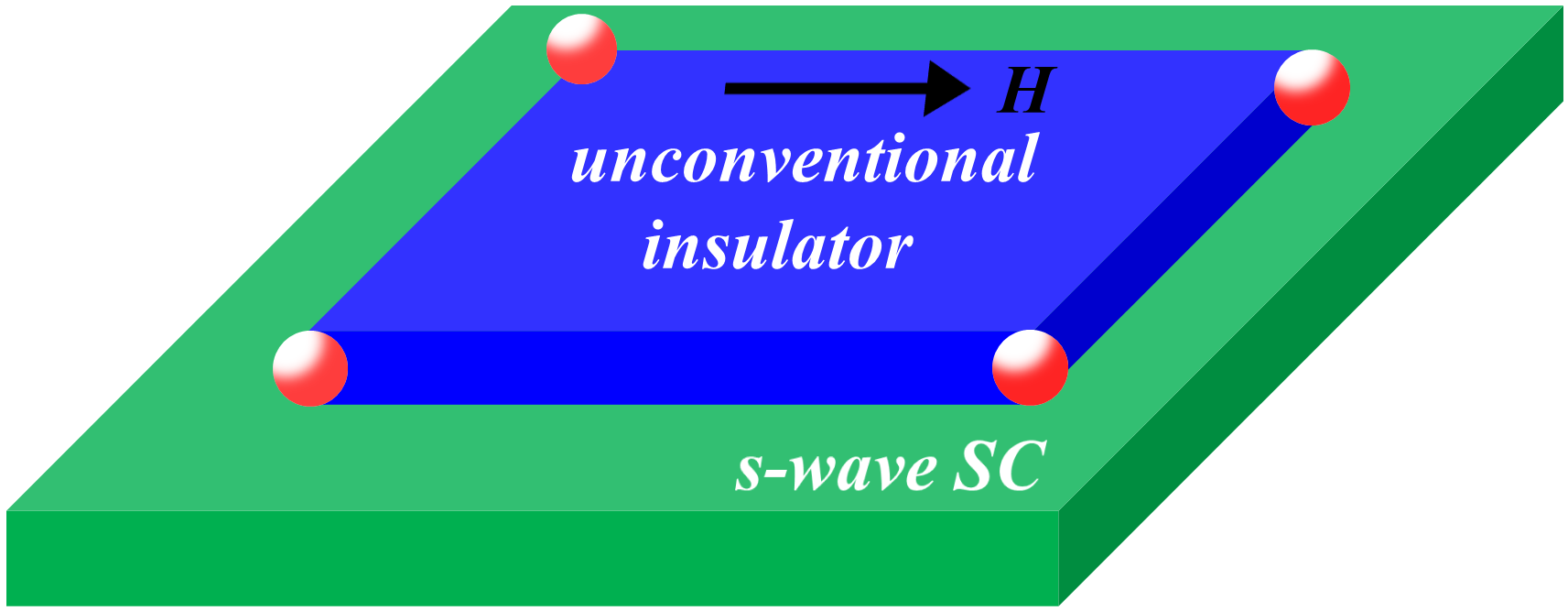
Majorana zero modes (MZMs) in topological superconductors Alicea (2012) have attracted great interest in the past two decades and an amount of physical systems Kitaev (2001); Fu and Kane (2008); Liu and Trauzettel (2011); Oreg et al. (2010); Lutchyn et al. (2010); Tewari and Sau (2012) have been proposed to realize Majorana modes. Among them, the Rashba semiconducting nanowire, which hosts Majorana end states with superconducting proximity and under magnetic field, is a well-studied system Alicea et al. (2011); Mourik et al. (2012). Recently, the idea of higher-order topological superconductors Langbehn et al. (2017); Xie et al. (2023) broadens the researching area of Majoranas and turns the Majorana modes to corners and hinges. Normally, higher-order topological superconductivity always requires either unconventional pairing order Zhu (2018); Pahomi et al. (2020); Yan et al. (2018); Wang et al. (2018); Liu et al. (2018); Zhang et al. (2019a); Zhang and Das Sarma (2021) (-, - or -wave) or complicated junctions Volpez et al. (2019), which are difficult to implement in experiment. By use of topologically protected edge states of quantum spin Hall insulators in proximity contact with an -wave superconductor, Majorana corner modes can be realized when subjecting to external magnetic field or ordering Wu et al. (2020); Zhang et al. (2019b). However, the obstructed edge states of unconventional/obstructed materials Nie et al. (2021); Gao et al. (2022); Xu et al. (2021a); Bradlyn et al. (2017); Po et al. (2018); Song et al. (2020); Xu et al. (2021b); Li et al. (2022); Shao et al. (2023); Zhang et al. (2023a); Xu et al. (2022); Zhang et al. (2023b); Wu et al. (2022); Yang et al. (2023), viewed as a one-dimensional (1D) system existing strong Rashba band splitting, also have potential to host Majorana corner modes, which has not been explored yet [Fig. 1].
As a representative of 1T-phase transition metal dichalcogenides ( Ni, Pd, Pt; S, Se, Te), 1T-PtSe2 shows many excellent characteristics, like high electron mobility Zhao et al. (2017), helical spin texture Yao et al. (2017), unique magnetic ordering Avsar et al. (2020), and excellent photocatalytic activity Yeliang et al. (2015), etc Zhang et al. (2017); Lin et al. (2017); Tyner and Goswami (2023). Recently, the edge electronic states of PtSe2 zigzag ribbon have been predicted theoretically Liu and Liu (2018) and subsequently confirmed experimentally Wang et al. (2022). The PtSe2 ribbon is demonstrated to grow naturally along the zigzag direction, and the edge states make few-layer PtSe2 more semi-metallic Wang et al. (2022); Kempt et al. (2023). However, the formation mechanism of the edge states is still unrevealed.
In this work, we first propose that MZMs can be realized at the corners of the unconventional 1T-PtSe2 monolayer. Based on the first-principles calculations, we demonstrate that 1T-PtSe2 is a symmetry indicator-free (SI-free) unconventional insulator. The new kind of unconventionality is not indicated by any symmetry eigenvalues, but directly diagnosed by the computed Wannier charge centers. Our detailed analysis shows that the unconventional nature is attributed to the splitting of the band representation (BR) of Se states. The obstructed edge states exhibit strong anisotropy and large Rashba splitting. By introducing superconducting proximity and external magnetic field, the MZMs can be generated at the corners of 1T-PtSe2 monolayer.
| Atom | WKS() | Symm. | Conf. | Irreps() | ABRs() |
|---|---|---|---|---|---|
| Pt | -3m | : | |||
| (000) | : | ||||
| : | |||||
| Se | 3m | : | |||
| - | : |
Electronic band structure and band representation analysis.
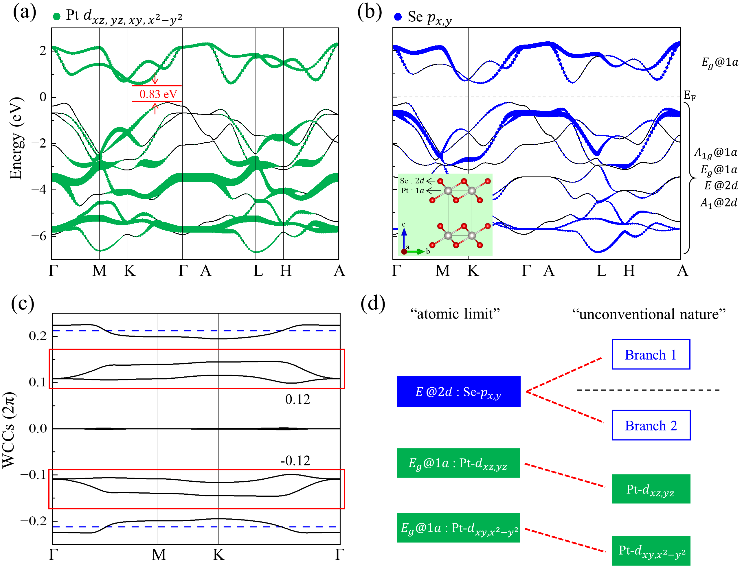
The 1T-phase PtSe2 possesses a structure with space group , where each Pt atom lies at the center of an octahedral cage formed by Se atoms, as shown in inset of Fig. 2(b). The layers are connected by van der Waals force. The Pt and Se atoms are located at the and Wyckoff positions, respectively. In topological quantum chemistry theory Bradlyn et al. (2017), the BR is induced by the -irreducible representation (irrep) orbital at site, which also indicates a set of -irreps in momentum space. The generators of the BRs are elementary band representations (EBRs). Atomic valence-electron band representations (ABRs) are defined as the BRs induced by the atomic valence electrons. In PtSe2, all the low energy bands originate from the valence electrons of Pt and Se orbitals, which form the ABRs of the compound. These ABRs are generated by POS2ABR and presented in TABLE 1. The band structure of PtSe2 is obtained with an indirect gap of 0.83 eV in Fig. 2(a). Based on symmetry eigenvalues (or irreps), the nine valence bands can be decomposed to the sum of ABRs: , while the two conduction bands belong to Bradlyn et al. (2017); Po et al. (2017). They are exactly the obtained ABRs of TABLE 1. The ABRs decomposition seems consistent with the valence states of Pt4+ and Se2-, implying that the Se orbitals are fully occupied and two conduction bands are mainly from the Pt orbitals of the irrep.
| Branch 1 | Branch 2 | |
|---|---|---|
| (identical to ) | ||
| A A | A | A |
| H H H3 | H3 | H H2 |
| K K K3 | K3 | K K2 |
| L L L L | L L | L L |
| M M M M | M M | M M |
SI-free unconventional nature.
On the other hand, we calculate the orbital-resolved band structures in Figs. 2(a,b). The Pt orbitals form two irreps at site (being ABR), while the Se orbitals form an irrep at site (being ABR). Fig. 2(a) shows most weights of the -irrep Pt orbitals below the Fermi level (). In contrast, many weights of the -irrep Se orbitals are above the in Fig. 2(b). These results are not consistent with Pt4+ and Se2- states at all.
By using 1D Wilson loop method Wieder et al. (2020); Lin et al. (2023), the -directed Wannier charge centers (WCCs) are computed, indicating the electronic locations directly. The bands should have three WCCs at , while the bands should have WCCs at [dashed lines in Fig. 2(c)], being align with Se positions. The WCCs for nine occupied bands are obtained in Fig. 2(c), and the results show that the average of the two Wilson bands in the red boxes is , quite away from the Se atoms. It indicates the unconventional nature of charge mismatch in PtSe2. This SI-free unconventionality is not protected by any symmetry, being of accidental obstructed atomic limit.
Origin of unconventional nature.
To investigate the origin of unconventional nature, we have checked the irreps very carefully, because only the bands of the same irreps can hybridize. The schematic of band hybridization in PtSe2 is given in Fig. 2(d). Starting from the atomic limit, the energy levels of orbitals () are lower than that of orbitals () in the Wannier-based tight-binding Hamiltonian extracted from the density functional theory calculations, giving rise to a half filling of ABR at . Then, the ABR can be decomposed into two separate branches with branch 1 is identical to , as presented in TABLE 2. Due to the hybridization between Pt ()and Se (branch1 of ), branch 1 is fully unoccupied and branch 2 is fully occupied. The hybridization process gives rise to the SI-free unconventionality with the offset charge centers, which is diagnosed by WCCs in the 1D Wilson loop method.
Although it seems that the SI-free unconventionality can be removed by changing the relative onsite energy without closing the energy gap, the substitution with the same group elements usually doesn’t qualitatively change the relative onsite energy at all. As a matter of fact, all the 1T- compounds of PtSe2 family possess the SI-free unconventionality. First, the onsite energy of orbitals is lower than that of orbitals for all 1T- members at the atomic limit. Second, the interlayer hybridization of orbital may lead the metallicity in some 1T- compounds Sheng et al. (2023), which doesn’t really affect the SI-free unconventionality (relying on the and orbitals). As a result, the obstructed edge states are always expected. Recently, the existence of SI-free unconventionality and obstructed hinge states is demonstrated in NiTe2 bulk, and the magnetic field filtering of hinge supercurrent in NiTe2-based Josephson junctions is observed experimentally Le et al. (2023).
Obstructed edge states.
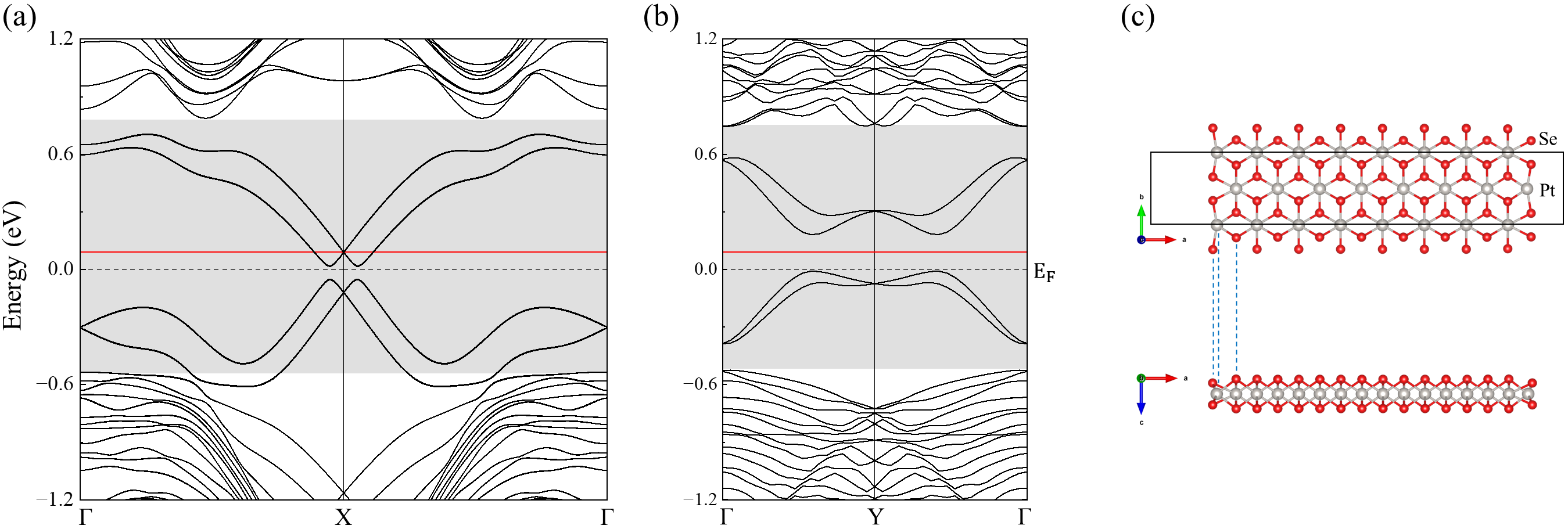
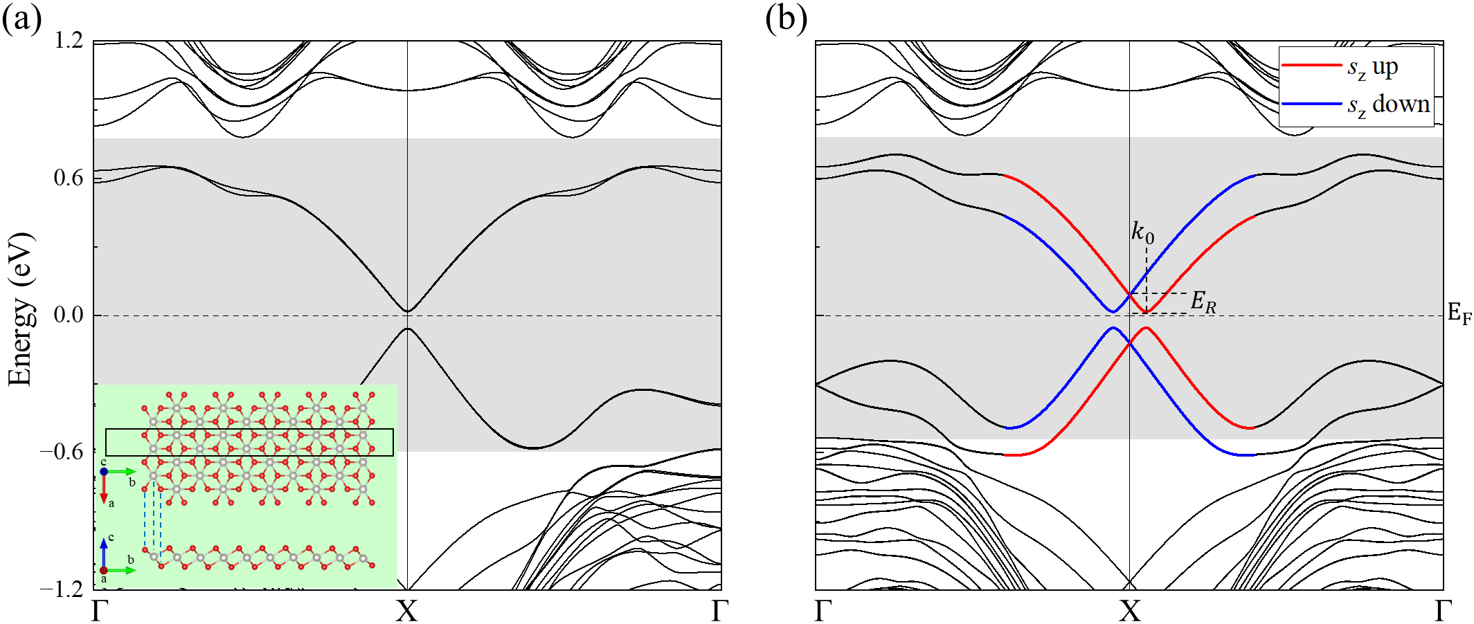
Due to the unconventional nature of the electronic band structure, obstructed edge states can emerge. The band structure of the zigzag edge ( direction) is presented in Fig. 3. Without spin-orbit coupling (SOC), the edge states appear in the bulk band gap (shadowed area), as shown in Fig. 3(a). The obstructed edge states behave as a massive Dirac band around X point, rather than a parabolic band, because the linear dispersion survives in a wide range () of the edge Brillouin zone. The gap of the edge Dirac band is 0.07 eV. The edge gap is consistent with the previous theoretical and experimental results Liu and Liu (2018); Wang et al. (2022); Kempt et al. (2023). In addition, the band structure of the armchair edge ( direction) is also obtained in Fig. S1 of the Supplementary Material (SM). Instead of a massive Dirac band, the obstructed edge states show an ‘M’-shaped band. Moreover, the armchair edge gap is larger than the zigzag edge gap, exhibiting strong anisotropy.
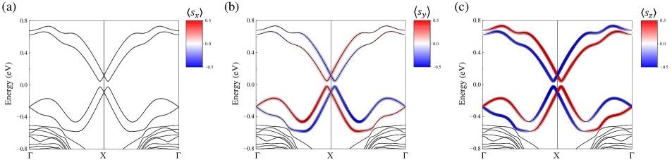
Once including SOC, the zigzag edge states will split into two massive Dirac bands, exhibiting large Rashba splitting in Fig. 3(b). The coupling strength of the Rashba SOC can be obtained as eVÅ, where Å and denote the momentum offset and Rashba energy, respectively. The remarkable is as large as those in the BiTeI Cai et al. (2022) and Bi/Ag(111) surface alloy Ast et al. (2007). As a result, two massive Dirac bands are supposed to have the opposite spin. Due to the coexistence of time reversal and symmetries, is required. However, and are allowed, which are computed in Fig. S2 of the SM. The -directed magnetic field can easily lift the Kramers’ degeneracy at X point. Since the component is dominant near the , the up and down states are depicted in Fig. 3(b). We conclude that the obstructed edge states exhibit large Rashba splitting and strong anisotropy. The edge atoms of ribbons are fully relaxed in the calculations. These results are obtained by the ab initio calculations self-consistently.
Proposal for MZMs.
Due to the existence of obstructed edge states with large Rashba splitting and strong anisotropy, we propose that the MZMs can be realized at the corners of 1T-PtSe2 monolayer. Under an -wave superconducting proximity and -directed magnetic field, the zigzag edge can be tuned to an equivalent spinless -wave Kitaev chain Kitaev (2001), while the armchair edge is fully gapped (Fig. S1 in the SM). Thus, at the corners (ends of the zigzag edge), MZMs can be realized with a proper chemical potential. It is proposed for the first time that MZMs exist at the corners of the two-dimensional (2D) topologically trivial insulator with unconventionality.
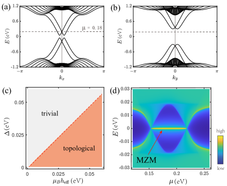
To simulate the Majorana corner modes in the system, we construct a 2D lattice model, consisting of two copied of Bernevig-Hughes-Zhang (BHZ) Hamiltonians,
| (1) | ||||
Here, (). Pauli matrices , and act on BHZ, orbital, and spin spaces, respectively. adds energy difference between the two copies of BHZ states. generates the anisotropy on two different edges. indicates the hybridization between the two Dirac states on the edges. These parameters are estimated by fitting the band structure from the first-principles calculations. In Figs. 4 (a,b), we plot the -directed (ZZ) and -directed (AC) edge dispersions. In the two-BHZ model, when tuning the chemical potential to the degenerate states on ZZ edge, there are no Fermi-level states on AC edge [ eV; the dashed line in Figs. 4 (a,b)]. Therefore, only the ZZ edge responds to the external magnetic field and superconducting proximity. Both the Zeeman coupling and superconducting paring order can open an energy gap at . Particularly, they are competing with each other, giving rising to the phase diagram in Fig. 4(c). When the Zeemann gap is dominant at , the ZZ edge becomes an equivalent spinless -wave Kitaev system. In the topological region, we demonstrate that superconducting proximity can induce MZMs as shown in Fig. 4(d), which are bounded to the corners.
Discussion.
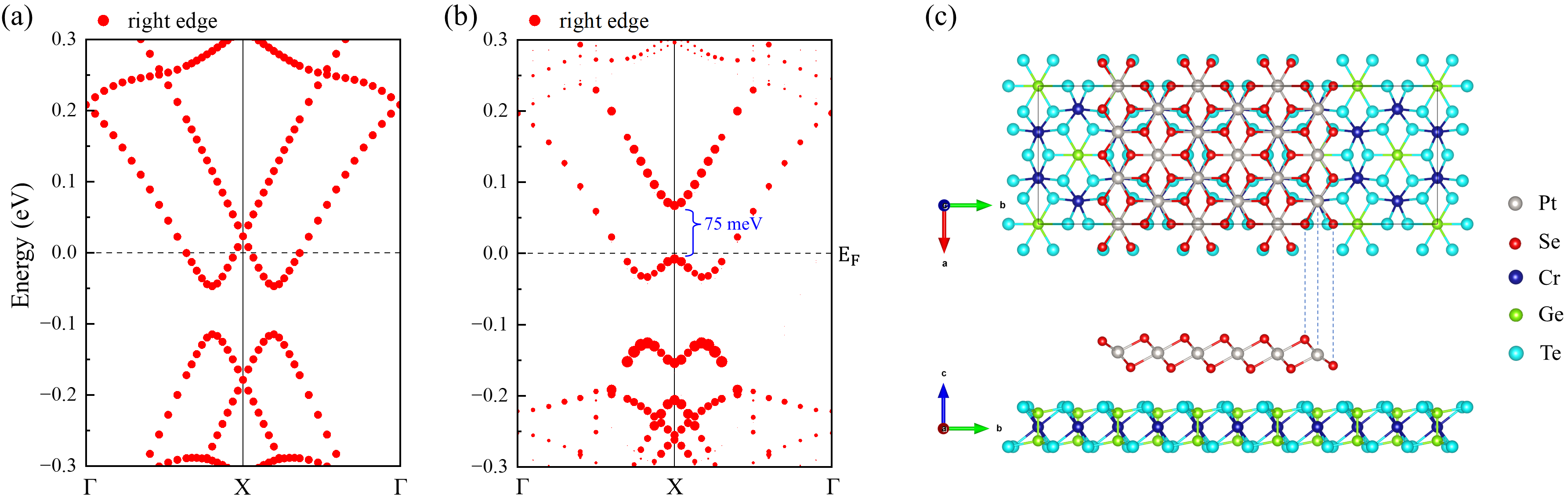
To realize the Majorana corner modes in 1T-PtSe2 monolayer, the effective -factor of the zigzag edge states is important; in other words, the gap due to external magnetic field at X point does matter in this proposal. Here, we propose that the ferromagnetic insulator CrGeTe3 is a proper substrate to induce the magnetic gap on the zigzag edge of 1T-PtSe2 monolayer. The results of Fig. S3 in the SM show that the -directed magnetic moment of CrGeTe3 substrate can cause a large Zeeman gap of 75 meV at X point. Covered by a conventional -wave Bardeen-Cooper-Schrieffer superconductor, e.g. Aluminum, the MZMs at the corners of 1T-PtSe2 monolayer are experimentally accessible.
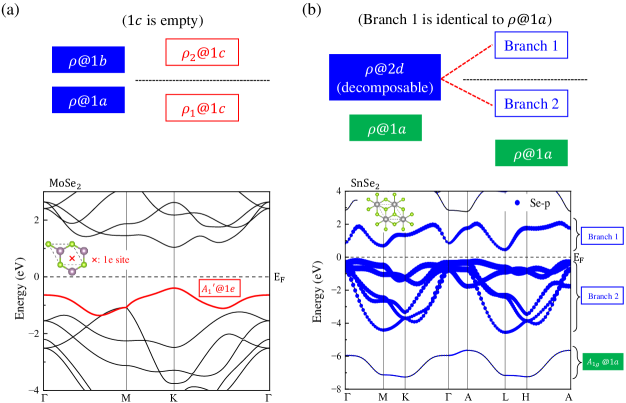
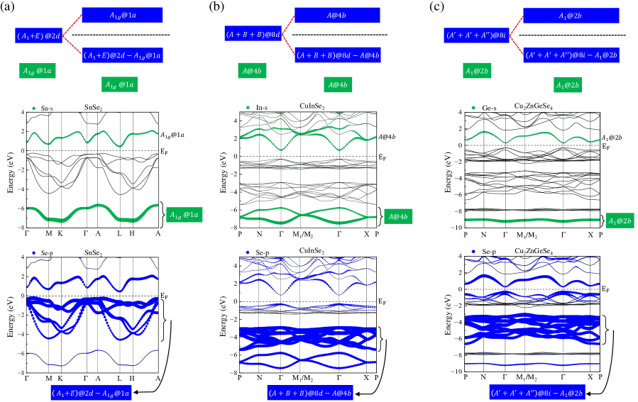
The SI-free unconventionality of charge mismatch is proposed for the first time and doesn’t have any symmetry eigenvalue indication Po et al. (2017), analogue to SI-free topological insulators. But it can be directly diagnosed by the computed WCCs by using the 1D Wilson loop method. Another type of unconventionality with an empty-site EBR has the symmetry indication in Fig. S4 of the SM. We demonstrate that the SI-free unconventionality is attributed to the splitting of the decomposable BR with band hybridization. The SI-free unconventionality widely exists in the compounds with (Ga/In)3+ or (Ge/Sn)4+ valence states, which suggest that the -orbital states would be empty and all above the . On the contrary, the results show that these states are quite far below the . The detailed BR analyses and orbital-resolved band structures of SnSe2, CuInSe2, and Cu2ZnGeSe4 are presented in Fig. S5 of the SM. These SI-free unconventional compounds have exhibited superconductivity Lochocki et al. (2019); Song et al. (2019), and optoelectronic or solar cell applications Li et al. (2015); Choubrac et al. (2020) in experiment.
In this work, we demonstrate that 1T-PtSe2 is an SI-free unconventional insulator, whose unconventional nature originates from the band hybridization between Pt and Se states. The obstructed electronic states on the zigzag edge exhibit large Rashba splitting. With the high mobility and large Zeeman gap on the magnetic substrate CrGeTe3, the MZMs at the corners of 1T-PtSe2 monolayer are experimentally accessible. Additionally, our two-BHZ model is first proposed to capture the Majorana corner modes in the unconventional monolayer with anisotropy. Our proposal for the Majorana corner modes in a topologically trivial system with anisotropy can be widely used in experiment.
Acknowledgments.
This work was supported by the National Natural Science Foundation of China (Grants No. 11974395, No. 12188101), the Strategic Priority Research Program of Chinese Academy of Sciences (Grant No. XDB33000000), National Key R&D Program of Chain (Grant No. 2022YFA1403800), and the Center for Materials Genome.
References
- Alicea (2012) J. Alicea, Reports on Progress in Physics 75, 076501 (2012).
- Kitaev (2001) A. Y. Kitaev, Physics-Uspekhi 44, 131 (2001).
- Fu and Kane (2008) L. Fu and C. L. Kane, Phys. Rev. Lett. 100, 096407 (2008).
- Liu and Trauzettel (2011) C.-X. Liu and B. Trauzettel, Phys. Rev. B 83, 220510 (2011).
- Oreg et al. (2010) Y. Oreg, G. Refael, and F. von Oppen, Phys. Rev. Lett. 105, 177002 (2010).
- Lutchyn et al. (2010) R. M. Lutchyn, J. D. Sau, and S. Das Sarma, Phys. Rev. Lett. 105, 077001 (2010).
- Tewari and Sau (2012) S. Tewari and J. D. Sau, Phys. Rev. Lett. 109, 150408 (2012).
- Alicea et al. (2011) J. Alicea, Y. Oreg, G. Refael, F. von Oppen, and M. P. A. Fisher, Nature Physics 7 (2011), 10.1038/nphys1915.
- Mourik et al. (2012) V. Mourik, K. Zuo, S. M. Frolov, S. R. Plissard, E. P. A. M. Bakkers, and L. P. Kouwenhoven, Science 336, 1003 (2012).
- Langbehn et al. (2017) J. Langbehn, Y. Peng, L. Trifunovic, F. von Oppen, and P. W. Brouwer, Phys. Rev. Lett. 119, 246401 (2017).
- Xie et al. (2023) Y. Xie, X. Wu, Z. Fang, and Z. Wang, “Hybrid topological superconductivity and hinge majorana flat band in type-ii dirac semimetals,” (2023), arXiv:2303.11729 [cond-mat.supr-con] .
- Zhu (2018) X. Zhu, Phys. Rev. B 97, 205134 (2018).
- Pahomi et al. (2020) T. E. Pahomi, M. Sigrist, and A. A. Soluyanov, Phys. Rev. Res. 2, 032068 (2020).
- Yan et al. (2018) Z. Yan, F. Song, and Z. Wang, Phys. Rev. Lett. 121, 096803 (2018).
- Wang et al. (2018) Q. Wang, C.-C. Liu, Y.-M. Lu, and F. Zhang, Phys. Rev. Lett. 121, 186801 (2018).
- Liu et al. (2018) T. Liu, J. J. He, and F. Nori, Phys. Rev. B 98, 245413 (2018).
- Zhang et al. (2019a) R.-X. Zhang, W. S. Cole, and S. Das Sarma, Phys. Rev. Lett. 122, 187001 (2019a).
- Zhang and Das Sarma (2021) R.-X. Zhang and S. Das Sarma, Phys. Rev. Lett. 126, 137001 (2021).
- Volpez et al. (2019) Y. Volpez, D. Loss, and J. Klinovaja, Phys. Rev. Lett. 122, 126402 (2019).
- Wu et al. (2020) Y.-J. Wu, J. Hou, Y.-M. Li, X.-W. Luo, X. Shi, and C. Zhang, Phys. Rev. Lett. 124, 227001 (2020).
- Zhang et al. (2019b) R.-X. Zhang, W. S. Cole, X. Wu, and S. Das Sarma, Phys. Rev. Lett. 123, 167001 (2019b).
- Nie et al. (2021) S. Nie, Y. Qian, J. Gao, Z. Fang, H. Weng, and Z. Wang, Phys. Rev. B 103, 205133 (2021).
- Gao et al. (2022) J. Gao, Y. Qian, H. Jia, Z. Guo, Z. Fang, M. Liu, H. Weng, and Z. Wang, Science Bulletin 67, 598 (2022).
- Xu et al. (2021a) Y. Xu, L. Elcoro, G. Li, Z.-D. Song, N. Regnault, Q. Yang, Y. Sun, S. Parkin, C. Felser, and B. A. Bernevig, “Three-dimensional real space invariants, obstructed atomic insulators and a new principle for active catalytic sites,” (2021a), arXiv:2111.02433 [cond-mat.mtrl-sci] .
- Bradlyn et al. (2017) B. Bradlyn, L. Elcoro, J. Cano, M. Vergniory, Z. Wang, C. Felser, M. I. Aroyo, and B. A. Bernevig, Nature 547, 298 (2017).
- Po et al. (2018) H. C. Po, H. Watanabe, and A. Vishwanath, Phys. Rev. Lett. 121, 126402 (2018).
- Song et al. (2020) Z.-D. Song, L. Elcoro, and B. A. Bernevig, Science 367, 794 (2020).
- Xu et al. (2021b) Y. Xu, L. Elcoro, Z.-D. Song, M. G. Vergniory, C. Felser, S. S. P. Parkin, N. Regnault, J. L. Mañes, and B. A. Bernevig, “Filling-enforced obstructed atomic insulators,” (2021b), arXiv:2106.10276 [cond-mat.mtrl-sci] .
- Li et al. (2022) G. Li, Y. Xu, Z. Song, Q. Yang, Y. Zhang, J. Liu, U. Gupta, V. Sü, Y. Sun, P. Sessi, S. S. P. Parkin, B. A. Bernevig, and C. Felser, Advanced Materials 34, 2201328 (2022).
- Shao et al. (2023) D. Shao, J. Deng, H. Sheng, R. Zhang, H. Weng, Z. Fang, X.-Q. Chen, Y. Sun, and Z. Wang, Research 6, 0042 (2023).
- Zhang et al. (2023a) R. Zhang, J. Deng, Y. Sun, Z. Fang, Z. Guo, and Z. Wang, Phys. Rev. Res. 5, 023142 (2023a).
- Xu et al. (2022) Y. Xu, M. G. Vergniory, D.-S. Ma, J. L. Mañes, Z.-D. Song, B. A. Bernevig, N. Regnault, and L. Elcoro, “Catalogue of topological phonon materials,” (2022), arXiv:2211.11776 [cond-mat.mtrl-sci] .
- Zhang et al. (2023b) R. Zhang, H. Sheng, J. Deng, Z. Yang, and Z. Wang, “Unconventional phonon spectra and obstructed edge phonon modes,” (2023b), arXiv:2305.09453 [cond-mat.mtrl-sci] .
- Wu et al. (2022) H. Wu et al., Nature 604, 653 (2022).
- Yang et al. (2023) Z. Yang, H. Sheng, Z. Guo, R. Zhang, Q. Wu, H. Weng, Z. Fang, and Z. Wang, “Superconductivity in unconventional metals,” (2023), arXiv:2306.08347 [cond-mat.mtrl-sci] .
- Zhao et al. (2017) Y. Zhao, J. Qiao, Z. Yu, P. Yu, K. Xu, S. P. Lau, W. Zhou, Z. Liu, X. Wang, W. Ji, and Y. Chai, Advanced Materials 29, 1604230 (2017).
- Yao et al. (2017) W. Yao, E. Wang, H. Huang, K. Deng, M. Yan, K. Zhang, K. Miyamoto, T. Okuda, L. Li, Y. Wang, H. Gao, C. Liu, W. Duan, and S. Zhou, Nature Communications 8, 14216 (2017).
- Avsar et al. (2020) A. Avsar, C.-Y. Cheon, M. Pizzochero, M. Tripathi, A. Ciarrocchi, O. V. Yazyev, and A. Kis, Nature Communications 11, 4806 (2020).
- Yeliang et al. (2015) W. Yeliang, L. Linfei, Y. Wei, S. Shiru, S. J. T., P. Jinbo, R. Xiao, L. Chen, O. Eiji, W. Yu-Qi, W. Eryin, S. Yan, Z. Y. Y., Y. Hai-tao, S. Eike F., I. Hideaki, S. Kenya, T. Masaki, C. Zhaohua, Z. Shuyun, D. Shixuan, P. Stephen J., S. T. Pantelides, and G. Hong-Jun, Nano Lett. 15, 4013–4018 (2015).
- Zhang et al. (2017) K. Zhang, M. Yan, H. Zhang, H. Huang, M. Arita, Z. Sun, W. Duan, Y. Wu, and S. Zhou, Phys. Rev. B 96, 125102 (2017).
- Lin et al. (2017) X. Lin, J. C. Lu, Y. Shao, Y. Y. Zhang, X. Wu, J. B. Pan, L. Gao, S. Y. Zhu, K. Qian, Y. F. Zhang, D. L. Bao, L. F. Li, Y. Q. Wang, Z. L. Liu, J. T. Sun, T. Lei, C. Liu, J. O. Wang, K. Ibrahim, D. N. Leonard, W. Zhou, H. M. Guo, Y. L. Wang, S. X. Du, S. T. Pantelides, and H.-J. Gao, Nature Materials 16, 717 (2017).
- Tyner and Goswami (2023) A. C. Tyner and P. Goswami, “Solitons and real-space screening of bulk topology of quantum materials,” (2023), arXiv:2304.05424 [cond-mat.mtrl-sci] .
- Liu and Liu (2018) S. Liu and Z. Liu, Phys. Chem. Chem. Phys. 20, 21441 (2018).
- Wang et al. (2022) H. Wang, Z. Liu, Y. Sun, X. Ping, J. Xu, Y. Ding, H. Hu, D. Xie, and T. Ren, Nano Research 15, 4668 (2022).
- Kempt et al. (2023) R. Kempt, A. Kuc, T. Brumme, and T. Heine, “Edge conductivity in ptse2 nanostructures,” (2023), arXiv:2306.04365 [cond-mat.mtrl-sci] .
- Po et al. (2017) H. C. Po, A. Vishwanath, and H. Watanabe, Nature Communications 8, 50 (2017).
- Wieder et al. (2020) B. J. Wieder, Z. Wang, J. Cano, X. Dai, L. M. Schoop, B. Bradlyn, and B. A. Bernevig, Nature Communications 11, 627 (2020).
- Lin et al. (2023) K.-S. Lin, G. Palumbo, Z. Guo, Y. Hwang, J. Blackburn, D. P. Shoemaker, F. Mahmood, Z. Wang, G. A. Fiete, B. J. Wieder, and B. Bradlyn, “Spin-resolved topology and partial axion angles in three-dimensional insulators,” (2023), arXiv:2207.10099 [cond-mat.mes-hall] .
- Sheng et al. (2023) H. Sheng, Z. Fang, and Z. Wang, Phys. Rev. B 108, 104109 (2023).
- Le et al. (2023) T. Le, R. Zhang, C. Li, R. Jiang, H. Sheng, L. Tu, X. Cao, Z. Lyu, J. Shen, G. Liu, F. Liu, Z. Wang, L. Lu, and F. Qu, “Magnetic field filtering of the hinge supercurrent in unconventional metal nite2-based josephson junctions,” (2023), arXiv:2303.05041 [cond-mat.mes-hall] .
- Cai et al. (2022) L. Cai, C. Yu, W. Zhao, Y. Li, H. Feng, H.-A. Zhou, L. Wang, X. Zhang, Y. Zhang, Y. Shi, J. Zhang, L. Yang, and W. Jiang, Nano Letters 22, 7441 (2022), pMID: 36099337.
- Ast et al. (2007) C. R. Ast, J. Henk, A. Ernst, L. Moreschini, M. C. Falub, D. Pacilé, P. Bruno, K. Kern, and M. Grioni, Phys. Rev. Lett. 98, 186807 (2007).
- Lochocki et al. (2019) E. B. Lochocki, S. Vishwanath, X. Liu, M. Dobrowolska, J. Furdyna, H. G. Xing, and K. M. Shen, Applied Physics Letters 114 (2019), 10.1063/1.5084147, 091602.
- Song et al. (2019) Y. Song, X. Liang, J. Guo, J. Deng, G. Gao, and X. Chen, Phys. Rev. Mater. 3, 054804 (2019).
- Li et al. (2015) W. Li, Z. Pan, and X. Zhong, J. Mater. Chem. A 3, 1649 (2015).
- Choubrac et al. (2020) L. Choubrac, M. Bär, X. Kozina, R. Félix, R. G. Wilks, G. Brammertz, S. Levcenko, L. Arzel, N. Barreau, S. Harel, M. Meuris, and B. Vermang, ACS Applied Energy Materials 3, 5830 (2020).
- Blöchl (1994) P. E. Blöchl, Phys. Rev. B 50, 17953 (1994).
- Kresse and Joubert (1999) G. Kresse and D. Joubert, Phys. Rev. B 59, 1758 (1999).
- Kresse and Furthmüller (1996) G. Kresse and J. Furthmüller, Computational Materials Science 6, 15 (1996).
- Kresse and Furthmüller (1996) G. Kresse and J. Furthmüller, Phys. Rev. B 54, 11169 (1996).
- Perdew et al. (1996) J. P. Perdew, K. Burke, and M. Ernzerhof, Phys. Rev. Lett. 77, 3865 (1996).
- Gao et al. (2021) J. Gao, Q. Wu, C. Persson, and Z. Wang, Computer Physics Communications 261, 107760 (2021).
- Marzari et al. (2012) N. Marzari, A. A. Mostofi, J. R. Yates, I. Souza, and D. Vanderbilt, Rev. Mod. Phys. 84, 1419 (2012).
SUPPLEMENTARY MATERIAL
A Calculation and Methodology
We carried out the first-principles calculations based on the density functional theory (DFT) with projector augmented wave (PAW) method Blöchl (1994); Kresse and Joubert (1999), as implemented in the Vienna ab initio simulation package (VASP) Kresse and Furthmüller (1996, 1996). The generalized gradient approximation (GGA) in the form of Perdew-Burke-Ernzerhof (PBE) function Perdew et al. (1996) was employed for the exchange-correlation potential. The kinetic energy cutoff for plane wave expansion was set to 450 eV. The Brillouin zone was sampled by Monkhorst-Pack method in the self-consistent process, with a 181810 k-mesh for PtSe2 bulk and a 1011 (161) k-mesh for PtSe2 ribbon with zigzag (armchair) edge. The thickness of the vacuum layers along () and directions were set to > 20 Å for PtSe2 ribbon with zigzag (armchair) edge. The irreducible representations (irreps) of electronic states were obtained by the program IRVSP . The elementary band representations (EBRs)/atomic valence-electron band representations (ABRs) decomposition of the band structure is done on the UnconvMat website with the obtained tqc.data Gao et al. (2021). The maximally localized Wannier functions for the Pt and Se orbitals were constructed by using the Wannier90 package Marzari et al. (2012).