On-chip indistinguishable photons using III-V nanowire/SiN hybrid integration
Abstract
We demonstrate on-chip generation of indistinguishable photons based on a nanowire quantum dot. From a growth substrate containing arrays of positioned-controlled single dot nanowires, we select a single nanowire which is placed on a SiN waveguide fabricated on a Si-based chip. Coupling of the quantum dot emission to the SiN waveguide is via the evanescent mode in the tapered nanowire. Post-selected two-photon interference visibilities using continuous wave excitation above-band and into a p-shell of the dot were 100%, consistent with a single photon source having negligible multi-photon emission probability. Visibilities over the entire photon wavepacket, measured using pulsed excitation, were reduced by a factor of 5 when exciting quasi-resonantly and by a factor of 10 for above-band excitation. The role of excitation timing jitter, spectral diffusion and pure dephasing in limiting visibilities over the temporal extent of the photon is investigated using additional measurements of the coherence and linewidth of the emitted photons.
I Introduction
High interference visibility between two single photons incident on separate input ports of a 50/50 beamsplitter, the Hong-Ou-Mandel (HOM) effectHong et al. (1987), establishes the indistinguishable nature of the photons, an essential requirement in most photonic quantum technologiesO’Brien et al. (2009). Epitaxial semiconductor quantum dots offer a solid-state solution for deterministically generating indistinguishable photons Santori et al. (2002) with state-of-the-art sources demonstrating two-photon interference (TPI) visibilities in excess of 95% He et al. (2013); Ding et al. (2016); Somaschi et al. (2016) for pulse separations of over s Wang et al. (2016) in devices with efficiencies of up to 57% Tomm et al. (2021). These sources were designed to emit out-of-plane, whereas a key advantage of solid-state emitters is the ability to integrate them with on-chip photonic circuitryHepp et al. (2019). An integrated platform, whereby multiple sources generate indistinguishable photons Patel et al. (2010); Kim et al. (2016) propagating within on-chip photonic circuitry Ellis et al. (2018), is a long-term challenge addressing scalability requirements of complex quantum processing schemes O’Brien et al. (2009).
Two distinct technologies for generating on-chip indistinguishable photons using quantum dots are currently being pursued. In monolithic approaches Dietrich et al. (2016), the quantum dot is embedded within photonic crystal waveguides Kalliakos et al. (2014, 2016) or suspended nanobeams Prtljaga et al. (2016) fabricated from the same III-V material system. Hybrid platforms Elshaari et al. (2020), on the other hand, combine III-V-based quantum dot systems with Si-based integrated circuits in which the dot emission is coupled to waveguide structures using either direct butt-coupling Ellis et al. (2018) or evanescent fields Schnauber et al. (2018). Initial experiments Kalliakos et al. (2014, 2016); Prtljaga et al. (2016); Schnauber et al. (2019) demonstrating on-chip generation of indistinguishable photons using the above approaches relied on post-selected TPI visibilities where excitation was provided by a continuous wave (CW) laser. More recently, non-post-selected measurements made using resonant pulsed excitation have shown TPI visibilities of % between sequentially emitted photon separated by a few nanoseconds Kiršanskė et al. (2017); Dusanowski et al. (2019); Uppu et al. (2020a); Dusanowski et al. (2020) up to almost 800 ns Uppu et al. (2020b).
In this work we report on a deterministic hybrid technique for generating in-plane indistinguishable photons. We use position-controlled nanowire quantum dots Laferriére et al. (2022) incorporated in photonic nanowire waveguides that are designed for efficient evanescent coupling to SiN waveguidesMnaymneh et al. (2020). The approach is similar to previous techniques employing evanescent coupling of III-V structures to underlying Si-based photonic structures Kim et al. (2017); Davanco et al. (2017); Schnauber et al. (2018), except here the adiabatic mode transfer is not realized through geometries defined by lithography but rather by a taper introduced in the photonic nanowire during growth Dalacu et al. (2021). The hybrid construction relies on a pick and place technique whereby individual nanowires are picked up from the III-V growth substrate and placed on a SiN waveguide fabricated on a Si wafer. The transfer is carried out in a scanning electron microscope (SEM) which provides a placement precision of a few nanometers; a positioning control sufficient to achieve optimal nanowire-waveguide coupling.
We obtain peak TPI visibilities of over the temporal extent of the emitted photons when exciting non-resonantly. To gain insight into the the different mechanisms limiting the observation of high visibilities, we perform additional experiments sensitive to decoherence processes in two-level systems: first-order correlation, , and high resolution spectroscopic measurements.
II Chip-integrated nanowire source
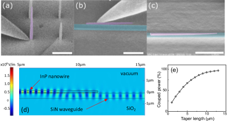
The quantum dots used in this work are sections of InAsP incorporated within position-controlled InP nanowires grown using gold-catalyzed vapour-liquid-solid epitaxy described in detail in Refs. 30; 31; 32. The nanowires are clad with an InP shell to create a photonic nanowire with a base diameter of 250 nm that supports single mode waveguiding of 1.3 eV photons. The photonic nanowire is tapered to a tip diameter of 100 nm over a m length (see Fig. 1(a)) to enable adiabatic mode transfer, discussed below. The low-loss photonic circuitry was fabricated in SiN grown by low-pressure chemical vapour deposition with measured propagation loss dB/cm at 965 nm. Waveguide dimensions were 400 nm wide and 485 nm thick with SiO2 below and above, designed to support a single polarization mode at 1.3 eV. The SiN waveguides were terminated at etched facets of the Si chip where the width was tapered to 250 nm for efficient coupling to single mode lensed fibres (SMLF) with measured coupling losses of dB/facet.
The nanowires were transferred to the Si chip pre-fabricated with the SiN photonic circuitry using an SEM-based nanomanipulator as shown in Fig. 1(a)-(c). A single nanowire is picked up from the growth substrate with a tungsten tip controlled by piezo-motors and then moved to the Si chip mounted next to the growth substrate. The nanowire is then placed either on or beside a selected SiN waveguide which has been exposed by opening a m2 window in the top oxide, see Fig. 2(a). As mentioned above, the nanowires are tapered to promote adiabatic mode transfer from the InP nanowire to the SiN waveguide. In Fig. 1(d) we show a simulation of the HE11 mode in the nanowire transfer to the TE mode in the SiN waveguide. From this we calculate a transfer efficiency in excess of 90% for the nanowire geometry specified above but with a waveguide design that supports both TE and TM polarizations.
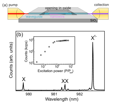
The chip was cooled to 4 K in a fibre-coupled closed-cycle He cryostat equipped with xyz piezo stages for fibre-waveguide alignment. The nanowires were optically excited through the waveguide via a SMLF. The emission was collected on the other end of the waveguide through another SMLF and directed to a fibre-coupled grating spectrometer equipped with a nitrogen-cooled charge-coupled device for spectrally resolved measurements or to superconducting nanowire single photon detectors (SNSPD, timing jitter 100 ps) via a fibre-coupled tunable filter (bandwidth = 0.1 nm) for measurements on single lines. An s-shell photoluminescence (PL) spectrum from the on-chip source is shown in Fig. 2(b) and displays the typical exciton complexes (, , ) observed from such nanowire quantum dotsLaferriére et al. (2021).
In this article, we focus on the emission. We first determine the efficiency of single photon generation from the device. For pulsed above-band excitation at 80 MHz, we measure a maximum of 0.919 Mcps at the SNSPD detector at an excitation power that saturates the transition, see inset in Fig. 2(b). Taking into account the optical throughput of the system (8.1%) and the detector efficiency (88.5%), both measured at 980 nm, we obtained a first-lens count rate of 12.9 Mcps, corresponding to source efficiency of . To estimate the dot to SiN waveguide coupling, we consider () a calculated dot-HE11 coupling of %Dalacu et al. (2019), () a 50% loss of photons for emission directed towards the base of the nanowire, () a 50% loss due to the waveguide design which only supports one of the two polarization modes in the nanowire, and () a 20% loss of photons emitted into phonon sidebandsDalacu et al. (2019) which are filtered-out. Taking into account these losses, we obtain an evanescent coupling efficiency of , slightly lower than both the calculations shown in Fig. 1(e) and our best measured results to date, (see Ref. 35). The lower than predicted values may be associated with emission into other charge complexesLaferriére et al. (2022), e.g. the neutral complexes and , evident in Fig. 2(b).
III TPI measurements: CW excitation
To measure TPI visibilities, the polarization of the photons are first aligned to the slow axis of a polarization-maintaining (PM) fibre using a fibre paddle polarization controller and filtered using the tunable filter to isolate the line. The photons are then input to a PM fibre-based unbalanced Mach-Zehnder interferometer (MZI) equipped with two fibre-coupled free-space non-polarizing beamsplitters (BS1 and BS2) each with a 50:50 nominal splitting ratio, see Fig. 3(a). Two additional polarizers are placed on each arm of the MZI to ensure linear polarized photons incident on BS2. One arm of the MZI includes a half-wave plate (HWP) for controlling the relative polarizations, , of the photons incident on the input ports of BS2. The delay between the two arms of the interferometer, , is adjusted by adding additional fibre to one of the arms. Two SNSPD detectors at the output ports of BS2, labelled ‘start’ and ‘stop’, together with counting electronics are used to register coincidences.
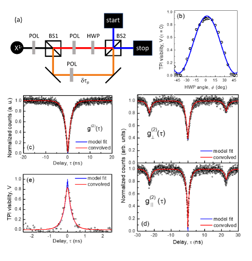
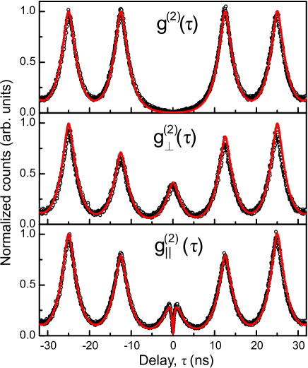
We discuss first measurements performed using CW excitation. We verified the performance of the interferometer by measuring the dependence of the TPI visibility at ns on , given by . This is plotted in Fig. 3(b) (black symbols), measured using above-band CW excitation and a delay of ns. We observe an expected oscillatory behaviour in the visibility, from to , as is varied from to . The maximum visibility observed is limited by the detector response, discussed below.
To determine the TPI visibilities as a function of delay , coincidence spectra are measured for cross- () and co-linear () polarized photons incident on BS2, and , respectively, and the visibilities are calculated from
| (1) |
Typical spectra are shown in Figs. 3(d) (black symbols) for measurements made using above-band CW excitation at and a delay ns.
To model the coincidence spectra, we examine the four possible path combinations two photons can take to traverse the MZI and arrive simultaneously at BS2 at . Consider first the 2 cases where the photons are incident on different input ports of BS2 (e.g. the photons travel in different arms of the MZI). If the pair is distinguishable (e.g. in the polarization degree of freedom by setting ) each photon is equally likely to be reflected or transmitted, and of the four possible outcomes, only the two where the photons exit different ports will register coincidence counts at zero delay. This is the case in the upper panel of Fig. 3(d) which shows a relative to the coincidence counts at long delays from uncorrelated photons. If the pair is indistinguishable, these two outcomes will destructively interfere (i.e. the incident pair coalesces, always exiting the same port) so that there are no possible outcomes that can register a coincidence at zero delay. This is the case in the lower panel of Fig. 3(d) which shows a . The other two cases, where the photons travel in the same arm of the MZI, will have both photons incident on the same port of BS2. Since the photons are generated by the same single photon source, they cannot arrive simultaneously, hence will not register zero-delay coincidences.
The absence of simultaneous photons incident on BS1 also eliminates one of the four possible outcomes that would lead to coincidences at . This manifests as a reduction in to at that is seen in Fig. 3(d).
For 50:50 beamsplitters, the behaviour above can be modelled by
| (2) |
| (3) |
which describe the cross-polarized, , and co-polarized, , coincidences, respectively, in terms of the second-order correlation function . The first (second) term in Eqns. 2 and 3 accounts for the cases where the photons are incident on the same (different) input port(s) of BS2 whilst accounts for the spatial overlap of the photons on BS2 which is assumed to be 100% (i.e. ). The time-scale represents, phenomenologically, the temporal extent over which photons incident on BS2 will coalesce, providing a measure of the probability of coalescence. The functional form with which it is incorporated in Eq. 3 will depend on the mechanism limiting coalescence e.g. homogeneous versus inhomogeneous broadening. For simplicity, we use an exponential decay (i.e. the visibility is limited by pure dephasingBylander et al. (2003)) though we do expect spectral diffusion to play a role due to the non-resonant excitation.
In this work we use a modified model which explicitly includes the transmission (, ) and reflection (, ) coefficients of BS1 and BS2:Patel et al. (2008)
| (4) |
| (5) |
The additional terms are required to account for deviations from a perfect, loss-less system, deviations which result in coincidence dip depths that differ from the values described above. For example, if T, then the drop in coincidences at will be less than 25%, and, in the case of distinguishable photons, . For , there will be an asymmetry in the depths of the side dips. Although there is little evidence of the latter in the measured spectra (i.e. ), we do observe values of which we associate not necessarily to an unbalanced BS1, but to a difference in the propagation losses between the two arms of the MZI (e.g. from inclusion of the components and accompanying mating sleeves) that result in different count rates incident on the two ports of BS2.
To reproduce the experimental and using Eqns. 4 and 5, we first measure by detecting coincidences at the two output ports of BS1. The measured under the same operating conditions as the HOM experiment shown in Fig. 3(d) is shown in Fig. 3(c) (black symbols). The response is modelled using (see Supplemental Materialat http://link.aps.org/ for additional measurements. ) where the radiative lifetime, ns, is independently measured and the excitation rate, , is a fit parameter. The blue curve in the figure shows the model fit using .
This expression of is incorporated in Eqns. 4 and 5 which are then applied to the measured correlations and with and the beamsplitter coefficients as fit parameters. The resulting fits are shown in Fig. 3(d) (blue curves) where, for this particular measurement (above-band CW excitation at and ns delay) we obtain a ratio of 0.25:0.75, a ratio of 0.48:0.52 and ns.
The visibility obtained from Eqn. 1 using the model correlations is shown in Fig. 3(e) (blue curve) and, by definition, predicts a TPI visibility . To match experiment, we convolve the model correlations with a 100 ps Gaussian detector response function and obtain the red curves in Figs. 3 (c)-(e) which correctly predict the measured raw visibility .
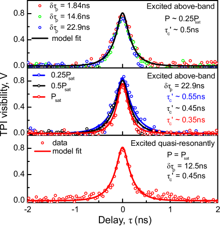
We have performed the above analysis on measurements taken under different operating conditions to extract values. The results are summarized in Fig. 4. For measurements as a function of using above-band CW excitation at (upper panel) we obtained ns, independent of path delay for ns to 22.9 nm. This suggests that the mechanisms limiting values occur on time-scales faster than ns. In contrast, from measurements as a function of excitation power (middle panel), we observed a significant increase in from 0.35 ns to 0.55 ns for a four-fold reduction in power. We also observed a moderate increase in when we excite quasi-resonantly into a p-shell of the dot. For measurements at , ns for p-shell excitation (bottom panel) compared to ns for above-band excitation.
Although CW HOM measurements reveal the presence of decoherence mechanisms through the measurement of , to extract meaningful values requires simultaneous fitting of the three correlations , and measured under the same operating conditions. Without the additional information provided by , erroneous values of are possible due the dependence of the antibunching dip in CW measurements on the excitation rate , see, for example, Ref. 33 and Supplemental Materialat http://link.aps.org/ for additional measurements. , Fig. S1. Finally we note that in all cases if account is taken of the detector response. This is expected in CW HOM measurements if , as is the case here i.e. is only limited by the detector responsePatel et al. (2008); Ates et al. (2009); Patel et al. (2010).
IV TPI measurements: pulsed excitation
To evaluate non-post-selected visibilities e.g. over the temporal extent of the emitted photons, we perform the same TPI measurements using pulsed excitation which allows one to quantify the probability of emitting identical photons and will also be ultimately required for on-demand operation. Using a tunable pulsed laser (pulse width ps) we measure visibilities as in the previous section, for both above-band and quasi-resonant excitation. We use a pulse repetition rate of 80 MHz, i.e. a pulse period of 12.5 ns, and a corresponding delay in one arm of the MZI of ns. The measured coincidences , and (black symbols) for the case of quasi-resonant excitation at are shown in Fig. 5.
Similar to the case of CW excitation for a nominal interferometer (50:50 beamsplitters, 100% transmission), if two photons arriving simultaneously at BS2 are distinguishable we expect a peak centred at zero delay having half the height of the peaks at whilst the peaks at should be reduced by 25%. For two perfectly indistinguishable photons arriving at BS2, the zero-delay peak should be absent. The measured (middle panel in figure) qualitatively reproduces the behaviour expected of impinging distinguishable photons on BS2. For the indistinguishable case, however, the zero-delay peak in the measured (bottom panel in figure) is still present but with a dip that drops to zero coincidences at . This behaviour is well documentedFlagg et al. (2010); Gold et al. (2014); Huber et al. (2015); Reimer et al. (2016); Weber et al. (2018) and is a consequence of processes that limit coalescence to time-scales shorter than the temporal extent of the photons e.g. () pure dephasingLegero et al. (2003), () spectral diffusionKambs and Becher (2018) and () excitation timing jitterKiraz et al. (2004), and thus limit extracted to values less then . We note that the last mechanism, timing jitter, is the primary distinction between the pulsed and CW measurements: it is absent in the latter where the experiment selects only the photons that arrive simultaneously at BS2.
As in the CW case, the curves in Fig. 5 are modelled using Eqns. 4 and 5 but with the latter modified toat http://link.aps.org/ for additional measurements. :
| (6) |
such that is simply given by less the exponential term defining the time-scale over which the photons coalesce. This is seen clearly for the case of nominal 50:50 beamsplitters in which case Eq. 6 reduces to after setting .
The that is incorporated in Eqs. 4 and 6 is constructed from peaks described by , i.e. we self-convolve model fits to measured time-resolved PL spectra, see Supplemental Materialat http://link.aps.org/ for additional measurements. , Fig. S2. This allows us to account for the dependence of the peaks on operating conditions through , the time-scale associated with preparation of the state. We neglect re-excitation which reduces the single photon purity to and assume a in the zero delay peak. The resulting fits are shown in the figure (red curves) where, as for the CW measurements, we have fit the beam splitter ratios and . We note that for the pulsed measurements we obtained slightly different beam splitter ratios for cross- and co-linear measurements which is evident in the data from the pronounced asymmetry between the peaks at in the whereas these peaks are symmetric in correlations. For the particular measurement shown in Fig. 5, i.e. quasi-resonant excitation at , we obtain a ratio of 0.27:0.73 (0.31:0.69) and ratio of 0.35:0.65 (0.5:0.5) for () and ns.
In Fig. 6 we plot a zoom-in of the the zero-delay peaks for both cross- and co-linear measurements, and respectively, for quasi-resonant (upper panel) and above-band (lower panel) excitation. The raw visibility over the temporal extent of the emitted photons is determined as in the previous section using Eqn. 1 but here we use the integrated coincidence counts over . Under quasi-resonant excitation at we obtain a non-post-selected visibility of . If the contributions to the coincidence counts from the correlation side peaks are removed (see right panel of figure), we obtain a corrected visibility (e.g. the visibility that would result using a longer pulse period ) of . In this plot we have also corrected for non-nominal values of the beam splitter ratios for comparison with the above-band measurements, discussed below.
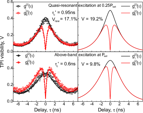
For above-band excitation (lower panel of Fig. 6) the zero-delay peak is significantly broader than that observed when exciting quasi-resonantly (e.g. compare (black curves)) and the dip at is significantly narrower (compare (red curves)). Both broadening of the peak and narrowing of the dip (quantified by the reduced ns) are a consequence of the more significant timing jitterLegero et al. (2006) present in above-band excitation i.e. longer time-scale associated with the state preparation , since above-band excitation includes additional processes related to carrier thermalization and capture not present for quasi-resonant excitation. We note that here we have used a higher excitation power than that used in the quasi-resonant measurement and this will also contribute to a decrease in , as observed in the CW measurements.
We also observe that for the above-band measurements the zero-delay peaks of cross- and co-linear correlations do not overlap at values away from . This is a consequence of the more significant difference in the beam splitter ratios between the respective measurements and strongly impacts the calculated visibility using the raw data. Instead we calculate and using the fit value of but with 50:50 beam splitter ratios as above. For the above-band non-post-selected visibility we obtain , substantially lower compared to the quasi-resonant case and consistent with the reduced value.
Comparison with previously reported values is restricted due to the dependence of measured visibilities on both excitation conditions Huber et al. (2015); Reindl et al. (2019) and the delay between interfered photons, Thoma et al. (2016). For above-band excitation, the only reported values, to our knowledge, are from our previous workReimer et al. (2016) where visibilities of were measured. There, a temporal delay of ns was used and the devices were grown at lower temperature where more severe linewidth broadening is expected, see Ref. 51. In the case of p-shell excitation with ns, similar visibilities, in the range , have been previously reported Gschrey et al. (2015); Thoma et al. (2016); Wang et al. (2016) including from on-chip sourcesKiršanskė et al. (2017).
V Coherence measurements
In this section we determine the coherence properties of the two-level excitonic system. We show results in the time-domain where coherence times, , are extracted from single photon interference visibilities e.g. measurements. We also compare with results in the frequency domain, where coherence times are extracted from linewidth measurements.
V.1 Interferometric measurements
For the time-domain measurements, the MZI was balanced (e.g. ) and a motorized fibre-based delay stage with a tuning range of 1.2 ns was added to one arm. The stage was scanned across it’s full range and at selected delays, , the fringe visibility was determined using a phase modulator in one arm of the MZI. The fringe visibility as a function of extracted from above-band and quasi-resonant measurements are plotted in Fig. 7.
For a homogeneously broadened transition i.e. the spectral linewidth of the emitted photons corresponds to the natural linewidth, the lineshape is Lorentzian and the visibility is expected to decay exponentially with a time constant . In the presence of inhomogeneous broadening, the decay will have a Gaussian componentBerthelot et al. (2006), , and is more appropriately described by a Voigt profileReimer et al. (2016):
| (7) |
We model the above-band fringe visibility using Eqn. 7 (curves in the upper panel of Fig. 7) to extract and . To compare with linewidth measurements below, we also calculated the full width at half maximum (FWHM) of the Voigt profile in the frequency domain given by
| (8) |
where is the Lorentzian contribution to the linewidth and is the Gaussian contribution. The extracted Voigt linewidths, , using above-band excitation are plotted in Fig. 9 (filled symbols).
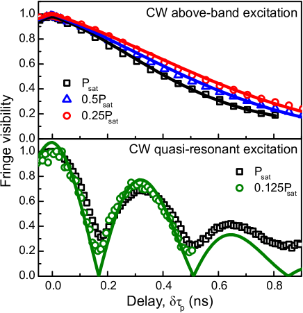
In the case of the quasi-resonant measurements (lower panel of Fig. 7), instead of a simple decay in the visibility with , we observe oscillatory behaviour indicative of a beating phenomenon. Why this arises is discussed below; here we simply assume the presence of two lines with frequency separation and identical coherence and model this behaviour by multiplying Eqn. 7 by the beating term . We only model the measurement at : at higher excitation powers (e.g. ) the assumption of identical coherence properties likely does not apply as suggested by the higher minima values in the visibility that are observed in the figure. The extracted from Eqn. 8 from the quasi-resonant pump at is plotted in Fig. 9 (open symbol).
V.2 Linewidth measurements
In the frequency-domain, we measure the linewidth of the emitted photons using a fibre-based, piezo-controlled Fabry-Perot etalon (bandwidth: 250 MHz, free spectral range: 40.75 GHz). High-resolution spectra obtained by scanning the etalon through the emission peak are shown in Fig. 8 for CW above-band (upper panel) and quasi-resonant (lower panel) excitation at . For above-band excitation we observe a single peak as expected from a singly-charged complex whilst for quasi-resonant excitation the same emission line is a doublet with a splitting of GHz consistent with the beating frequency observed in the coherence measurements. Given that , the observation of two peaks suggests either two mutually exclusive excitonic complexes or the same excitonic complex with the electrostatic environment jumping between two possible states.
There are two possible reasons why the observation of either two complexes or the same complex in two environments would depend on the excitation energy. First, in quasi-resonant excitation, fewer carriers are introduced into the system, resulting in a different Fermi level profile compared to above-band excitation. This may modify the relative intensities of different charge complexes in time-integrated PL spectra, which we have previously observed. Second, there may be a single, defect-related trap sufficiently close to the dot such that a Stark-mediated shift of the emission energy of GHz will result depending on the occupation of the trap. In this scenario, for above-band excitation the trap occupation is constant on the time-scale of the measurement ( ms) whereas for quasi-resonant excitation, the occupation fluctuates on a much faster time-scale such that both emission energies are observed in the time-integrated PL.
The magnitude of the observed splitting depends on the quasi-resonant excitation power, decreasing by GHz as the power is increased from to . Such an excitation power-dependent splitting is consistent with carrier screening of the Stark field but difficult to explain in the case of two distinct complexes. We therefore attribute the two peaks observed when exciting quasi-resonantly to the same excitonic complex .
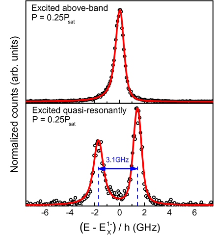
High resolution spectra were measured as a function of excitation power, deconvolved from the etalon response and fit using a Voigt lineshape. We note that the lineshapes obtained using above-band excitation present a slight asymmetry when excited at higher powers and these were fit with an asymmetric Voigt function. The origin of this asymmetry is unclear, but is typical of the nanowire quantum dot systemLaferrière et al. (2023a). The total linewidth from the fits are plotted in Fig. 9 for both the above-band (filled) and quasi-resonant (open) excitation. For clarity, only measurements of one of the two peaks observed with quasi-resonant excitation are included (the power-dependent linewidths of the second peak are similar).
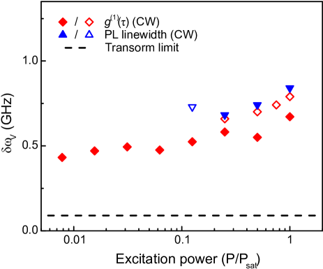
Comparison of the time- and frequency domain measurements reveal similar linewidths which do not depend significantly on the excitation energy: above-band (filled symbols) versus quasi-resonant (open symbols). The absence of any narrowing when exciting below-band is surprising: in fact, we observe a small increase in the measured linewidth for quasi-resonant excitation. This suggests that the mechanisms responsible for the excess broadening are unrelated to the much higher density of excess carriers or phonons introduced with above-band excitation.
In all cases, we observe a decrease in excess broadening at lower excitation powers with a minimum extracted linewidth of 4X the transform limit (dashed line in the figure). The reduction in linewidth with excitation power is expected from a reduction in both phonon-related pure dephasing and charge noise-related spectral diffusion. We do not attempt to quantify these two contributions in terms of the Lorentzian versus Gaussian contributions to the measured linewidth: although the total Voigt linewidth is considered accurate, the Lorentzian:Gaussian ratio likely has a large uncertainty.
VI Discussion
To compare the coherence measurements with the HOM results, we use and extracted from the and linewidth measurements to calculate a ‘coherence time’ given byKambs and Becher (2018)
| (9) |
The calculated values of from the three experiments are summarized in Fig. 10. All measurements give values of ns at which increase as the excitation power is reduced, consistent with the linewidth measurements in Fig. 9, but still well below the transform limit of .
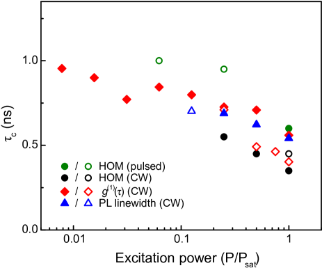
In the following we consider the distinct nature of each experiment to extract information on the nature of the mechanisms responsible for . We consider first the different time scales associated with each experiment. In the HOM measurement, different photons are interfered on a time-scale of 2-23 ns whilst in the coherence measurement, interference is between the same photon and the time-scale is 1.2 ns, but each point in the fringe visibility trace is a statistical average over ms. In the linewidth measurements, on the other hand, there is no interference, only a measure of the spectral purity over time-scales in the seconds. The consistency in the extracted coherence times irrespective of the experiment thus suggests that the mechanism(s) responsible for reducing values of below the transform limit of occur on a timescale of ns and there are no other mechanisms on longer time-scales for at least seconds.
Next we note the absence of any significant improvement in when switching from above-band to quasi-resonant excitation which is in stark contrast to other studiesHuber et al. (2015). This suggests that phonon dephasing is not the primary mechanism limiting the coherence times since the phonon occupation, by necessity, will be higher for above-band excitationLaferrière et al. (2023a). Which leaves spectral diffusion as the likely source, meaning the charge environment is equally stable, regardless of excitation mode.
Finally, we note that all the measurements with the exception of the pulsed HOM experiments, are independent of excitation jitter. And yet it is these measurements that produced the highest values of (compare, for example, pulsed versus CW HOM in Fig. 10). This suggest that either timing jitter is relatively unimportant or that pulsed excitation produces a more stable charge environment thus compensating for any reduction in due to timing jitter.
VII Conclusion
In summary, we have demonstrated the generation of indistinguishable photons on-chip based on the hybrid integration of positioned-controlled single quantum dot nanowires and silicon-based photonic integrated circuitryMnaymneh et al. (2020). Non-post-selected measurements over the photon lifetime revealed coalescence of only a small fraction of the emitted photons, . The TPI visibility was limited by the excess broadening that arises when exciting non-resonantly. Higher visibilities are anticipated with coherent excitation, as demonstrated in other quantum dot systemsHe et al. (2013); Ding et al. (2016); Somaschi et al. (2016).
The described integration approach provides a route to developing a platform whereby multiple sources of indistinguishable photons can be selectively incorporated on-chip, a long-term goal of future quantum technologies. As a final note, in this work we investigated nanowire quantum dots emitting at nm. However, the InAs/InP material system is also the ideal choice for generating telecom wavelengths and we have recently demonstrated high quality sources emitting in the O-bandLaferrière et al. (2023b). Using such emitters, the pick and place approach described here can be applied to the highly developed silicon-on-insulator integrated photonics platform.
Acknowledgments
This work was supported by the Natural Sciences and Engineering Research Council of Canada through the Discovery Grant SNQLS, by the National Research Council of Canada through the Small Teams Ideation Program QPIC and by the Canadian Space Agency through a collaborative project entitled ‘Field Deployable Single Photon Emitters for Quantum Secured Communications’. The authors would also like to thank Khaled Mnaymneh for assistance with the commercial foundry tape-out.
DATA AVAILABILITY
The data that support the findings of this study are available from the corresponding author upon reasonable request.
REFERENCES
References
- Hong et al. (1987) C. K. Hong, Z. Y. Ou, and L. Mandel, “Measurement of picosecond time intervals between two photons by interference.” Phys. Rev. Lett. 59, 2044–2046 (1987).
- O’Brien et al. (2009) J. L. O’Brien, A. Furusawa, and J. Vučković, “Photonic quantum technologies,” Nat. Photon. 3, 687 (2009).
- Santori et al. (2002) C. Santori, D. Fattal, J. Vučković, G. Solomon, and Y. Yamamoto, “Indistinguishable photons from a single-photon device,” Nature 419, 594–597 (2002).
- He et al. (2013) Y.-M. He, Y. He, Y.-J. Wei, D. Wu, M. Atatüre, C. Schneider, S. Höfling, M. Kamp, C.-Y. Lu, and J.-W. Pan, “On-demand semiconductor single-photon source with near-unity indistinguishability,” Nat. Nano. 8, 213–217 (2013).
- Ding et al. (2016) X. Ding, Y. He, Z.-C. Duan, N. Gregersen, M.-C. Chen, S. Unsleber, S. Maier, C. Schneider, M. Kamp, S. Höfling, C.-Y. Lu, and J.-W. Pan, “On-demand single photons with high extraction efficiency and near-unity indistinguishability from a resonantly driven quantum dot in a micropillar,” Phys. Rev. Lett. 116, 020401 (2016).
- Somaschi et al. (2016) N. Somaschi, V. Giesz, J.C. Loredo, M. P. Almeida, G. Hornecker, S.L. Portalupi, T. Grange, C. Antón, J. Demory, C. Gómez, I. Sagnes, N. D. Lanzillotti-Kimura, A. Lemaître, A. Auffèves, A. G. White, L. Lanco, and P. Senellart, “Near-optimal single-photon sources in the solid state,” Nat. Photon. 10, 340–345 (2016).
- Wang et al. (2016) H. Wang, Z.-C. Duan, Y.-H. Li, Si Chen, J.-P. Li, Y.-M. He, M.-C. Chen, Y. He, X. Ding, C.-Z. Peng, C. Schneider, M. Kamp, S. Höfling, C.-Y. Lu, and J.-W. Pan, “Near-transform-limited single photons from an efficient solid-state quantum emitter,” Phys. Rev. Lett. 116, 213601 (2016).
- Tomm et al. (2021) N. Tomm, A. Javadi, N. O. Antoniadis, D. Najer, M. C. Löbl, Al. R. Korsch, R. Schott, S. R. Valentin, A. D. Wieck, A. Ludwig, and R. J. Warburton, “A bright and fast source of coherent single photons,” Nature Nano. 16, 399 (2021).
- Hepp et al. (2019) S. Hepp, M. Jetter, S. L. Portalupi, and P. Michler, “Semiconductor quantum dots for integrated quantum photonics,” Adv. Quantum Technol. 2, 1900020 (2019).
- Patel et al. (2010) R. B. Patel, A. J. Bennett, I. Farrer, C. A. Nicoll, D. A. Ritchie, and A. J. Shields, “Two-photon interference of the emission from electrically tunable remote quantum dots,” Nat. Photonics 4, 632 (2010).
- Kim et al. (2016) J.-H. Kim, C. J. K. Richardson, R. P. Leavitt, and E. Waks, “Two-photon interference from the far-field emission of chip-integrated cavity-coupled emitters,” Nano Lett. 16, 7061 (2016).
- Ellis et al. (2018) D. J. P. Ellis, A. J. Bennett, C. Dangel, J. P. Lee, J. P. Griffiths, T. A. Mitchell, T.-K. Paraiso, P. Spencer, D. A. Ritchie, and A. J. Shields, “Independent indistinguishable quantum light sources on a reconfigurable photonic integrated circuit,” Appl. Phys. Lett. 112, 211104 (2018).
- Dietrich et al. (2016) C. P. Dietrich, A. Fiore, M. G. Thompson, M. Kamp, and S. Höfling, “Gaas integrated quantum photonics: Towards compact and multi-functional quantum photonic integrated circuits,” Laser and Photon. Rev. 10, 870 (2016).
- Kalliakos et al. (2014) S. Kalliakos, Y. Brody, A. Schwagmann, . J. Bennett, M. B. Ward, D. J. P. Ellis, J. Skiba-Szymanska, I. Farrer, J. P. Griffiths, G. A. C. Jones, D. A. Ritchie, and A. J. Shields, “In-plane emission of indistinguishable photons generated by an integrated quantum emitter,” Appl. Phys. Lett. 104, 221109 (2014).
- Kalliakos et al. (2016) S. Kalliakos, Y. Brody, A. J. Bennett, Da. J. P. Ellis, J. Skiba-Szymanska, I. Farrer, J. P. Griffiths, D. A. Ritchie, and A. J. Shields, “Enhanced indistinguishability of in-plane single photons by resonance fluorescence on an integrated quantum dot,” Appl. Phys. Lett. 109, 151112 (2016).
- Prtljaga et al. (2016) N. Prtljaga, C. Bentham, J. O’Hara, B. Royall, E. Clarke, L. R. Wilson, M. S. Skolnick, and A. M. Fox, “On-chip interference of single photons from an embedded quantum dot and an external laser,” Appl. Phys. Lett. 108, 251101 (2016).
- Elshaari et al. (2020) A. W. Elshaari, W. Pernice, K. Srinivasan, O. Benson, and Val Zwiller, “Hybrid integrated quantum photonic circuits,” Nature Photon. 14, 285 (2020).
- Schnauber et al. (2018) P. Schnauber, J. Schall, S. Bounouar, T. Höhne, S.-I. Park, G.-H. Ryu, T. Heindel, S. Burger, J.-D. Song, S. Rodt, and S. Reitzenstein, “Deterministic integration of quantum dots into on-chip multimode interference beamsplitters using in situ electron beam lithography,” Nano Lett. 18, 2336 (2018).
- Schnauber et al. (2019) P. Schnauber, A. Singh, J. Schall, , S.-I. Park, J.-D. Song, S. Rodt, K. Srinivasan, S. Reitzenstein, and M. Davanco, “Indistinguishable photons from deterministically integrated single quantum dots in heterogeneous gaas/si3n4 quantum photonic circuits,” Nano Lett. 19, 7164 (2019).
- Kiršanskė et al. (2017) G. Kiršanskė, H. Thyrrestrup, R. S. Daveau, C. L. Dreeßen, T. Pregnolato, L. Midolo, P. Tighineanu, A. Javadi, S. Stobbe, R. Schott, A. Ludwig, A. D. Wieck, S.-I. Park, J. D. Song, A. V. Kuhlmann, I. Söllner, M. C. Löbl, R. J. Warburton, and Peter P. Lodahl, “Indistinguishable and efficient single photons from a quantum dot in a planar nanobeam waveguide,” Phys. Rev. B 96, 165306 (2017).
- Dusanowski et al. (2019) Ł. Dusanowski, S.-H. Kwon, C. Schneider, and . Höfling, “Near-unity indistinguishability single photon source for large-scale integrated quantum optics,” Phys. Rev. Lett. 122, 173602 (2019).
- Uppu et al. (2020a) R. Uppu, H. T. Eriksen, H. Thyrrestrup, A. D. Uğurlu, Y. Wang, S. Scholz, A. D. Wieck, A. Ludwig, M. C. Löbl, . J. Warburton, P. Lodahl, and L. Midolo, “On-chip deterministic operation of quantum dots in dual-mode waveguides for a plug-and-play single-photon source,” Nature Commun. 11, 3782 (2020a).
- Dusanowski et al. (2020) Ł. Dusanowski, D. Köck, E. Shin, S.-H. Kwon, C. Schneider, and S. Höfling, “Purcell-enhanced and indistinguishable single-photon generation from quantum dots coupled to on-chip integrated ring resonators,” Nano Lett. 20, 6357 (2020).
- Uppu et al. (2020b) R. Uppu, F. T. Pedersen, . Wang, C. T. Olesen, C. Papon, X. Zhou, L. Midolo, S. Scholz, A. D. Wieck, . Ludwig, and P. Lodahl, “Scalable integrated single-photon source,” Sci. Adv. 6, eabc8268 (2020b).
- Laferriére et al. (2022) P. Laferriére, E. Yeung, I. Miron, D. B. Northeast, S. Haffouz, J. Lapointe, M. Korkusinski, P. J. Poole, R. L. Williams, and D. Dalacu, “Unity yield of deterministically positioned quantum dot single photon sources,” Sci. Rep. 12, 6376 (2022).
- Mnaymneh et al. (2020) K. Mnaymneh, D. Dalacu, J. McKee, J. Lapointe, S. Haffouz, J. F. Weber, D. B. Northeast, P. J. Poole, G. C. Aers, and R. L. Williams, “On-chip integration of single photon sources via evanescent coupling of tapered nanowires to sin waveguide,” Adv. Quantum Tech. 3, 1900021 (2020).
- Kim et al. (2017) J.-H. Kim, S. Aghaeimeibodi, C. J. K. Richardson, R. P. Leavitt, D. Englund, and E. Waks, “Hybrid integration of solid-state quantum emitters on a silicon photonic chip,” Nano Lett. 17, 7394–7400 (2017).
- Davanco et al. (2017) M. Davanco, J. Liu, L. Sapienza, C.-Z. Zhang, J. Vinícius De Miranda Cardoso, V. Verma, R. Mirin, S. Nam, L. Liu, and K. Srinivasan, “Heterogeneous integration for on-chip quantum photonic circuits with single quantum dot devices,” Nat. Commun. 8, 889 (2017).
- Dalacu et al. (2021) D. Dalacu, P. J. Poole, and R. L. Williams, “Tailoring the geometry of bottom-up nanowires: Application to high efficiency single photon sources,” Nanomaterials 11, 1201 (2021).
- Dalacu et al. (2009) D. Dalacu, A. Kam, D. G. Austing, X. Wu, J. Lapointe, G. C. Aers, and P. J. Poole, “Selective-area vapour-liquid-solid growth of InP nanowires,” Nanotech. 20, 395602 (2009).
- Dalacu et al. (2011) D. Dalacu, K. Mnaymneh, X. Wu, J. Lapointe, G. C. Aers, P. J. Poole, and R. L. Williams, “Selective-area vapor-liquid-sold growth of tunable inasp quantum dots in nanowires,” Appl. Phys. Lett. 98, 251101 (2011).
- Dalacu et al. (2012) D. Dalacu, K. Mnaymneh, J. Lapointe, X. Wu, P. J. Poole, G. Bulgarini, V. Zwiller, and M. E. Reimer, “Ultraclean emission from InAsP quantum dots in defect-free wurtzite InP nanowires,” Nano Lett. 12, 5919–5923 (2012).
- Laferriére et al. (2021) P. Laferriére, E. Yeung, M. Korkusinski, P. J. Poole, R. L. Williams, D. Dalacu, J. Manalo, M. Cygorek, A. Altintas, and P. Hawrylak, “Systematic study of the emission spectra of nanowire quantum dots,” Appl. Phys. Lett. (2021).
- Dalacu et al. (2019) D. Dalacu, P. J. Poole, and R. L. Williams, “Nanowire-based sources of non-classical light,” Nanotechnology 30, 232001 (2019).
- Yeung (2021) E. Yeung, Hybrid Integration of Quantum Dot-Nanowires with Photonic Integrated Circuits, Master’s thesis, University of Ottawa, 75 Laurier Ave. E, Ottawa, Canada, K1N 6N5 (2021).
- Bylander et al. (2003) J. Bylander, I. Robert-Philip, and I. Abram, “Interference and correlation of two independent photons,” Eur. Phys. J. D 22, 295–301 (2003).
- Patel et al. (2008) R. B. Patel, A. J. Bennett, K. Cooper, P. Atkinson, C. A. Nicoll, D. A. Ritchie, and A. J. Shields, “Postselective two-photon interference from a continuous nonclassical stream of photons emitted by a quantum dot,” Phys. Rev. Lett. 100, 207405 (2008).
- (38) See Supplemental Material at http://link.aps.org/ for additional measurements., .
- Ates et al. (2009) S. Ates, S. M. Ulrich, S. Reitzenstein, A. Löffler, A. Forchel, and P. Michler, “Post-selected indistinguishable photons from the resonance fluorescence of a single quantum dot in a microcavity,” Phys. Rev. Lett. 103 (2009).
- Flagg et al. (2010) E. B. Flagg, A. Muller, S. V. Polyakov, A. Ling, A. Migdall, and Glenn S. Solomon, “Interference of single photons from two separate semiconductor quantum dots,” Phys. Rev. Lett. 104, 137401 (2010).
- Gold et al. (2014) P. Gold, A. Thoma, S. Maier, S. Reitzenstein, C. Schneider, S. Höfling, and M. Kamp, “Two-photon interference from remote quantum dots with inhomogeneously broadened linewidths,” Phys. Rev. B 89, 035313 (2014).
- Huber et al. (2015) Tobias Huber, Ana Predojević, Daniel Föger, Glenn Solomon, and Gregor Weihs, “Optimal excitation conditions for indistinguishable photons from quantum dots,” New J. Phys. 17, 123025 (2015).
- Reimer et al. (2016) M. E. Reimer, G. Bulgarini, A. Fognini, R. W. Heeres, B. J. Witek, M. A. M. Versteegh, A. Rubino, T. Braun, M. Kamp, S. Höfling, D. Dalacu, J. Lapointe, P. J. Poole, and V. Zwiller, “Overcoming power broadening of the quantum dot emission in a pure wurtzite nanowire,” Phys. Rev. B 93, 195316 (2016).
- Weber et al. (2018) J. H. Weber, J. Kettler, H. Vural, M. Müller, J. Maisch, . Jetter, S. L. Portalupi, and P. Michler, “Overcoming correlation fluctuations in two-photon interference experiments with differently bright and independently blinking remote quantum emitters,” Phys. Rev. B 97, 195494 (2018).
- Legero et al. (2003) T. Legero, T. Wilk, A. Kuhn, and G. Rempe, “Time-resolved two-photon quantum interference,” Appl. Phys. B 77, 797–208 (2003).
- Kambs and Becher (2018) B. Kambs and C. Becher, “Limitations on the indistinguishability of photons from remote solid state sources,” New J. Phys. 20, 115003 (2018).
- Kiraz et al. (2004) A. Kiraz, M. Atatüre, , and A. Imamoglu, “Quantum-dot single-photon sources: Prospects for applications in linear optics quantum-information processing,” Phys. Rev. A 69, 032305 (2004).
- Legero et al. (2006) T. Legero, T. Wilk, A. Kuhn, and G. Rempe, “Characterization of single photons using two-photon interference,” Adv. At., Mol., Opt. Phys. 53, 253 (2006).
- Reindl et al. (2019) Marcus Reindl, Jonas H. Weber, Daniel Huber, Christian Schimpf, Saimon F. Covre da Silva, Simone L. Portalupi, Rinaldo Trotta, Peter Michler, , and Armando Rastelli, “Highly indistinguishable single photons from incoherently excited quantum dots,” Phys. Rev. B 100, 155420 (2019).
- Thoma et al. (2016) A. Thoma, P. Schnauber, M. Gschrey, M. Seifried, J. Wolters, J.-H. Schulze, A. Strittmatter, S. Rodt, A. Carmele, A. Knorr, T. Heindel, and S. Reitzenstein, “Exploring dephasing of a solid-state quantum emitter via time- and temperature-dependent hong-ou-mandel experiments,” Phys. Rev. Lett. 116, 033601 (2016).
- Laferrière et al. (2023a) Patrick Laferrière, Aria Yin, Edith Yeung, Leila Kusmic, Marek Korkusinski, Payman Rasekh, David B. Northeast, Sofiane Haffouz, Jean Lapointe, Philip J. Poole, Robin L. Williams, and Dan Dalacu, “Approaching transform-limited photons from nanowire quantum dots excited above-band,” Phys. Rev. B xx, xxxx (2023a).
- Gschrey et al. (2015) M. Gschrey, A. Thoma, P. Schnauber, M. Seifried, R. Schmidt, B. Wohlfeil, L. Krüger, J.-H. Schulze, T. Heindel, S. Burger, F. Schmidt, A. Strittmatter, S. Rodt, and S. Reitzenstein, “Highly indistinguishable photons from deterministic quantum-dot microlenses utilizing three dimensional in situ electron-beam lithography,” Nat. Commun. 6, 7662 (2015).
- Berthelot et al. (2006) A. Berthelot, I. Favero, G. Cassabois, C. Voisin, C. Delalande, Ph. Roussignol, R. Ferreira, and J. M. Gérard, “Unconventional motional narrowing in the optical spectrum of a semiconductor quantum dot,” Nature Physics 2, 759 (2006).
- Laferrière et al. (2023b) Patrick Laferrière, Sofiane Haffouz, David B Northeast, Philip J Poole, and Robin L Williams Dan Dalacu, “Position-controlled telecom single photon emitters operating at elevated temperatures,” Nano Lett. 23, 962–968 (2023b).