Constrained Bayesian Optimization Using a Lagrange Multiplier Applied to Power Transistor Design
Abstract
We propose a novel constrained Bayesian Optimization (BO) algorithm optimizing the design process of Laterally-Diffused Metal-Oxide-Semiconductor (LDMOS) transistors while realizing a target Breakdown Voltage (). We convert the constrained BO problem into a conventional BO problem using a Lagrange multiplier. Instead of directly optimizing the traditional Figure-of-Merit (FOM), we set the Lagrangian as the objective function of BO. This adaptive objective function with a changeable Lagrange multiplier can address constrained BO problems which have constraints that require costly evaluations, without the need for additional surrogate models to approximate constraints. Our algorithm enables a device designer to set the target in the design space, and obtain a device that satisfies the optimized FOM and the target constraint automatically. Utilizing this algorithm, we have also explored the physical limits of the FOM for our devices in 30 - 50 V range within the defined design space.
I Introduction
Efficient power electronics are an essential component of a society powered by renewable energy. Power semiconductor devices have been extensively adapted in all applications that require electrical power. Different materials such as siliconBaliga (2010), Silicon carbide (SiC)Kimoto and Cooper (2014); She et al. (2017), and Gallium nitride (GaN)Meneghini et al. (2021); Chen et al. (2017), along with various device structures like power diodes, planar/trench Metal-Oxide-Semiconductor Field-Effect Transistors (MOSFETs)Williams et al. (2017a, b), and Insulated-Gate Bipolar Transistors (IGBTs)Iwamuro and Laska (2017); Khanna (2004), are utilized in the fabrication of a wide range of analog microchips, catering to the power needs of diverse power management applications. The choice of material and device structure depends on the operating voltage requirements and specific performance characteristics desired for each application. These technologies enable the provision of electrical power to various appliances and systems. Among all power semiconductor devices, silicon-based Laterally-Diffused Metal-Oxide-Semiconductor (LDMOS) transistors are the most popular device since they can be seamlessly integrated into Integrated Circuit (IC) technologyChen et al. (2021); Chou et al. (2012); Jin et al. (2017); Huang et al. (2014); Cha et al. (2016); Saadat et al. (2022, 2020), bringing economic benefits and being able to bridge an extensive voltage range.
The Figure-of-Merit (FOM) = is an important metric employed to assess the quality of power devices Huang (2004). This criterion reflects the maximum achievable power density in a power device which is crafted by specific materials. As the LDMOS transistor is integrated within the silicon process and widely used to design various devices working at different operating voltages, the design challenge for LDMOS transistors has shifted to minimize the at specific voltages to approach the material’s physical limits and reduce the cost simultaneously. This principle of device design, known as the ”power density scaling“ law has been consistently applied in the field of power device design. Following this law, consequently, the ongoing challenge in the industry lies in designing and optimizing different LDMOS transistors with disparate values within the same semiconductor process.
In Moore’s Law transistors, all parameters such as the operation voltage are chosen for accurate and efficient communication, aiming to reduce cost-per-transistor for every new technology node roa (2022). In power semiconductor technology, however, microchips process power flows across different voltage domains specific to each application. For instance, a laptop power converter must efficiently convert direct current (DC) power from a 12 V battery to drive a 1 V microprocessor. Similarly, automotive applications may require transient operation at 40 V or higher due to fault conditions which exist in the automotive environment. Power transistors must support a wide voltage range, and their breakdown voltage () needs to be substantially higher than the operating voltage to ensure reliability throughout their operation lifetime. For example, the laptop 12 V to 1 V DC power converter mentioned above may require > 30 V, whereas an automotive microchip that survives fault conditions at 40 V might need a device with > 55 V. Thus, the optimization of power transistors involves selecting a limited range of values, considering specific application requirements.
Bayesian optimization (BO) is a data-driven algorithm that efficiently determines the global extremum within a defined space while minimizing the number of evaluations required Garnett (2023); Frazier (2018). In recent years, BO has gained significant popularity as a replacement for grid search or random search in optimizing the architecture of different machine learning modelsBergstra and Bengio (2012); Snoek, Larochelle, and Adams (2012); Bergstra et al. (2011). Moreover, BO is being increasingly adopted in various research domains to accelerate the optimization process and enhance the development of their respective fields such as chemical synthesisShields et al. (2021), process of solar cellsXu et al. (2023), optimization of lithium-ion batteriesGaonkar et al. (2022), and drug discoveryGuan and Fu (2022). Ironically, in more mature fields like the semiconductor industry, due to its earlier development compared to the popularity of BO, there is relatively less use of BO or other artificial intelligence assisted tools. We have previously integrated different optimization algorithms with Technology computer-aided design (TCAD) simulations to automate the optimization of semiconductor devices Chuang et al. (2023). Among all these optimization algorithms, BO is the most data efficient method to integrate with TCAD device simulations.
TCAD simulation is an indispensable tool in semiconductor device manufacturing. Due to the high cost associated with semiconductor device fabrication, performing TCAD simulations and designing desired device characteristics is a crucial part of device fabrication. Skilled engineers perform a large number of TCAD simulations, often guided by design of experiments (DOE) approaches like factorial designs, response surface designs, or Taguchi designs Chelladurai et al. (2021); Kleijnen (2008). The combination of DOE and TCAD simulations requires significant manual intervention and human involvement in the process. By integrating BO with TCAD simulations, we can perform automated and globally optimized designs, accelerating the development process. However, while optimizing device design, constraints must be respected. e.g., when designing a power device, needs to be sufficiently high. Checking whether a constraint () is satisfied can be the most computationally expensive part of simulations. Previous constrained BO relies on different surrogate models to approximate both the output parameter () and the objective function (FOM) Gardner et al. (2014). However, this approach requires using multiple surrogate models, which increase the time and resources required for evaluations to solve such constrained BO problems.
In this paper, we propose a constrained BO process using a Lagrange multiplier. We apply the methodology to the optimization of an LDMOS transistors enabling the optimization of LDMOS transistors with a given breakdown voltage. We first show that the unconstrained BO yields a device with a breakdown voltage of 31 V but reveals no information about devices with of or . Next, we show that we can successfully constrain the and find high-FOM devices for and . Our results demonstrate that constrained BO can effectively accomplish the optimization of device designs with specific restrictions, and even explore the physical limits for a specific breakdown voltage range without requiring human intervention.
II Results
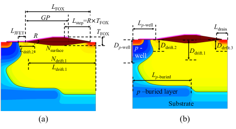
The LDMOS transistors under investigation are illustrated in Fig. 1. We use the standard Gaussian doping setting in the commercial simulation software to define all the doping profiles in this study Sen (2016). The elongated-diamond-shaped oxide region on the top of the device represents a LOCal-Oxidation Structure (LOCOS). The LOCOS acts as a field-relief oxide and increases the breakdown voltage when designed appropriately. The Junction Field-Effect-Transistor (JFET) region is located on the drift region which is not covered by the LOCOS. The fabrication process of LDMOS transistors with LOCOS can be found on Ref. Lik (2017). The doping concentration in the channel is chosen so that the leakage current remains smaller than A/m. The device under consideration has 19 parameters to define the device structure. For the BO, we optimize nine input parameters while keeping ten other input parameters fixed. For detail about constructing LDMOS transistors with LOCOS by 19 parameters in TCAD, we refer to the subsection IV.1.1.
The FOM = is the objective function of our unconstrained BO. , , and FOM are illustrated in the methodology section. The first 10 device configurations are chosen randomly followed by 190 or 790 new device structures generated iteratively using the acquisition function which maximizes the expected improvement of the FOM or the Lagrangian. Gaussian process regression is used to emulate the ground truth response surface in our design space. We first show the results of an unconstrained BO, followed by a constrained BO by developing a Lagrangian approach, finally we determine the frontier of the FOM vs .
Fig. 2 (a) exhibits the FOM and for 200 devices simulated in an unconstrained BO. The color of each marker indicates the order in which the devices are simulated with the darkest blue device simulated first, and the brightest red device simulated last. Most of the devices that are simulated last are found near the device with the highest FOM = 295 . This highest FOM device is found to have = 31 V. The vast majority of simulated devices have a < 31 V, a few high FOM devices are identified with while no high-FOM devices with are simulated during the BO. For applications requiring , the unconstrained FOM does not provide insight in device design.
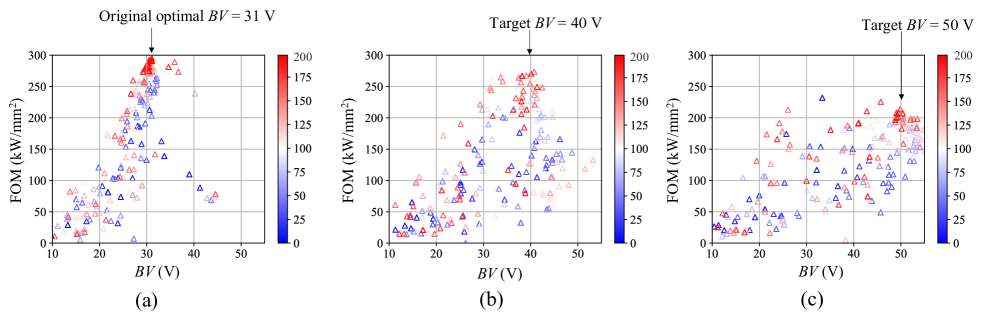
Fig. 2 (b) and (c) present 200 devices simulated in a constrained optimization with the target = 40 and 50 V constraints respectively. For the constrained BO, we use the same approach as for the unconstrained BO except that we optimize a Lagrangian function as detailed in the method section. Fig. 2 (b) has a maximum FOM = 270 W/ at = 41 V while Fig. 2 (c) has identified a FOM = 207 W/ device with a . The device with FOM = 207 W/ at is not the highest FOM device simulated in Fig. 2 (c) but it is the highest FOM device that can realize a breakdown voltage. Looking visually at the distribution of the devices in Fig. 2 (a) - (c), by adding the Lagrange term, many more devices with higher are simulated.
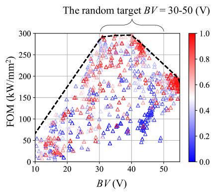
Fig. 3 reveals the frontier of FOM vs . We obtain the device configurations in Fig. 3 by performing a constrained BO where the constraint is changed at every iteration step. In each iteration, a target is chosen randomly between 30 V and 50 V and the acquisition function chooses a new design based on the Lagrange multiplier associated with the target of the current iteration and all previously acquired FOM and data. A total of 800 devices are simulated and the upper hull of the obtained results is indicated. Interestingly, the device with the highest FOM = 299 W/ is found to have a = 40 V, exceeding the best device we found from the unconstrained BO with 200 iterations in Fig. 2 (a). Within the design space that we have defined, we find that FOM 300 W/ devices can be designed with a = 30 V to = 40 V. Devices with a up to 55 V can be designed but the FOM would decrease to 200 W/.
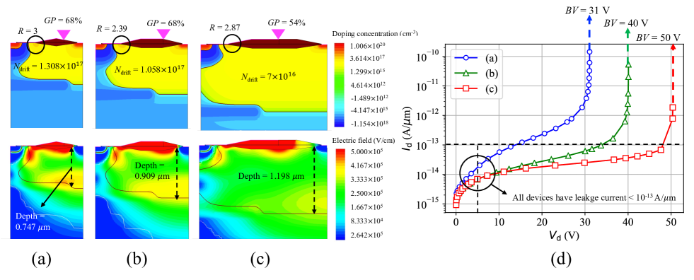
Fig. 4 (a) - (c) elucidate the device operation of the highest FOM device from the unconstrained BO, the constrained BO with and respectively. The figures on the upper row exhibit the doping profile, while the figures on the lower row are electrical field distributions at the breakdown condition. Inspecting the highest FOM device in the unconstrained BO, we find that the BO drives the device structure result on a diamond-shaped LOCOS as illustrated in Fig. 4 (a) compared to the elongated diamond-shapes in Fig. 4 (b) - (c). However, when constraining the to 40 V or 50 V, elongated-diamond shape devices are identified as having the highest FOM. Moreover, the results obtained from these algorithms align with the physical intuition of designers. For example, a higher device requires a lower drift doping concentration. The BO enables the automatic identification of which overall structure yields the highest FOM, without relying on time-consuming local/manual optimization.
III Discussion
Comparing the results in Fig. 2 and 3, we observe that for the 30 V optimized device, the FOM results are almost identical. However, when comparing the 40 V optimized device designs, we can see that the FOM in Fig. 2 (b) is approximately 270 W/, while it is around 299 W/ in Fig. 3. The higher FOM obtained in Fig. 3 is not entirely surprising because 800 iterations were used in Fig. 3 compared to the 200 for Fig. 2. Seemingly, the 30 BV region is easier to access for the BO compared to the 40 region. Nevertheless, from our study it appears that an informed constrained optimization can aid BO.
By adding a Lagrange multiplier to the BO, we have successfully been able to perform constrained BO. Specifically, using TCAD simulations, we have effectively been able to constrain the . Our problem is a specific example of a constraint that requires resource-intensive measurements or evaluations. A previous approach to constrained BO added an additional surrogate function to approximate the output Gardner et al. (2014), but in this approach, as the number of constrained output variables increases, more surrogate functions are needed to approximate each output individually. Our constrained BO algorithm is able to solve the specific design problem without any additional computational cost.
IV Methods
IV.1 TCAD simulation
IV.1.1 Device structure simulation
In Fig. 1 (a) Nine parameters are adjustable as input parameters for our TCAD simulations. 1) the peak doping concentration ( = ) of the first Gaussian doping, 2) the length of the first Gaussian doping peak line ( = ), 3) the length of the second Gaussian doping peak line ( = ), 4) the gate position ( = ), 5) the length of the JFET region ( = ), 6) the length of the FOX ( = ), 7) the doping concentration value on the surface of drift region ( = ), 8) the thickness of the FOX ( = ), 9) the shape ratio of LOCOS ( = ). Among these input parameters, , , , , are layout related parameters which can be defined by photo masks. Nevertheless, , , , are process related input parameters. The -type dose for the first Gaussian doping determines and . The local oxidation process determines and . The shape ratio () is defined to be equal to /, where is the taper length of LOCOS. is used to describe the shape of the bird’s beak which has significant impact on the performance of the LDMOS transistors. The larger causes a slender and elongated beak, whereas a smaller yields a shorter and stout beak. Therefore, various shapes of field oxide structures and doping profiles are considered in our simulations.
| Symbol (units) | Description | Bound |
|---|---|---|
| (cm-3) | The peak value of the 1st Gaussian doping | 7- 2.5 |
| (nm) | The length of the 1st Gaussian doping | 250 - 2700 |
| (nm) | The length of the 2nd Gaussian doping | 0 - 500 |
| (%) | Percentage of the FOX covered by the gate | 10 - 99 |
| (nm) | The length of JFET region | 0 - 700 |
| (nm) | The length of field oxide (FOX) | 750 - 2000 |
| (cm-3) | The doping concentration value on the surface of the drift region | 1- 6 |
| (nm) | The thickness of the FOX | 50 - 150 |
| The tangent of the angle of the FOX | 0.5 - 5 |
Fig. 1 (b) illustrates the fixed parameters during the optimization. We use a uniform -type with cm-3 doping concentration as the substrate. A -type buried layer with a doping concentration of cm-3 is introduced. The length of the -buried layer is fixed to = 0.95 m. A high -type doping concentration of cm-3 is applied on the surface as the -well for the LDMOS with a fixed depth = 0.4 m and a fixed length = 0.1 m. The first drift Gaussian doping peak is positioned at a depth of 0.3 m, forming the primary drift region. The second -type doping has a doping concentration of = , creating the channel in cooperation with the -well. The third -type doping is located beneath the drain region, and it shares the same doping concentration as the second -type doping. This arrangement serves to reduce the gradient of the doping concentration between the drain and the primary drift region so that the electric field on the drain side can be decreased. The thin gate oxide thickness is 12 nm. A LOCOS is implemented on top of the main drift region to increase the of the LDMOS transistors. The gate is placed on the elongated-diamond, allowing for the application of gate voltage stress on both the -well and the drift region to control the channel in on-state and electric field distribution on the device surface in off-state. The source and drain regions, featuring an -type doping concentration of , are positioned at the two terminals of the device with a same length = = 0.1 m. The definition of the half-pitch as the distance between the source and drain.
We minimize the number of input parameters in order to simplify the complexity of the TCAD simulation. Some parameters are dependent on defined input parameters. The depth of the drift region () is determined by the doping concentration value on the surface of the drift region () and the peak value of the first Gaussian doping () since the first doping profile is a Gaussian distribution. The depth of the drift region is equaling to
| (1) |
The thickness of the LOCOS () and the shape of tangent of the angle of the FOX () determines the taper length of LOCOS () in Fig.1 (a) through .
IV.1.2 TCAD Physical Models
For our simulations, we utilize a commercial drift-diffusion software with default silicon parametersSen (2016). To accurately capture various physical mechanisms, we use generation-recombination model, including the doping-dependent and the temperature-dependent Shockley-Read-Hall model, and the Auger model, each addressing specific aspects of carrier behavior and recombination processes. The van Overstraeten modelVan Overstraeten and De Man (1970) is used to account for the impact ionization process. To account for mobility degradation at the silicon-insulator interface, we employ the Lombardi model. In the bulk region, we utilize the widely accepted Philips unified mobility model, which provides a comprehensive description of carrier mobility. Carrier distributions are modeled using the Fermi-Dirac distribution, including the bandgap narrowing model.
IV.1.3 Device Characteristics
We define the breakdown voltage () and the specific on-resistance (). represents the maximum voltage between the source and drain that the device can sustain without experiencing avalanche breakdown when it is in the off-state. We perform the - measurement and ramp up the to extract the maximum when the TCAD no longer converges:
| (2) |
We calculate the specific on-state resistance () by
| (3) |
where is half-pitch (HP) times a unit length (default value is 1 m on the -direction since we are performing 2D simulations) and . We defined the current between source and drain as the leakage current . The leakage current is defined at in order to simplify the simulation process and shorten the simulation time. We fixed the -well doping profile and the second drift doping so that the channel length and the leakage current is fixed in all of our devices. All of our devices exhibit a leakage current less than /m. Leakage current is not the focus of our present study and could be further improved by adjusting the doping concentration of -well and the second Gaussian doping in the drift region.
Lastly, the FOM is the most important metric in this study, equaling
| (4) |
IV.2 Bayesian Optimization
For details of BO, we refer to Garnett (2023); Frazier (2018). We utilize the open-source package, skopt. We use Gaussian Process Regression (GPR) as the surrogate model and the Expected Improvement (EI) as the acquisition function. The radial basis function (RBF) kernel with length 1.0 is used in the GPR. For the acquisition function, the Limited-memory Broyden–Fletcher–Goldfarb–Shanno (L-BFGS) algorithm is used and 20 iterations are executed to find the extremum of the acquisition function.
IV.3 Lagrange Multiplier
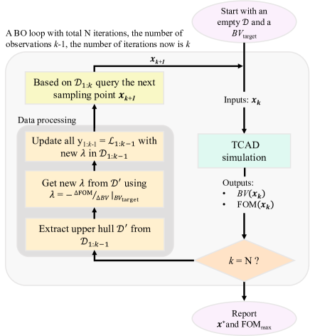
The algorithm flow chart for the constrained BO problem is shown in Fig. 5. The objective function of the BO is the Lagrangian
| (5) |
where is the Lagrange multiplier. In our specific problem and . The Lagrangian function reaches its optimum when . Note that when optimizing, is a constant and once is determined, the last term in Eq. (5) is just a constant which can be omitted without affecting the results. Correctly determining the Lagrange multiplier is critical.
We compute the Lagrange multiplier from the simulated data. We determine the devices that form the upper part of the convex hull that contains the FOM vs data, yielding a dataset , where is an index iterating over the data in the upper hull. The upper hull is illustrated in Fig. 3 where the upper part of the hull consists of a set of 5 points (). We then identify in which segment of the upper hull the target is located, i.e. , where is the number of the segments in the upper hull curve. Finally, the Lagrange multiplier is determined as
| (6) |
Acknowledgements.
The author also appreciates all of valuable discussion with Dr. Sujatha Sampath of Texas Instruments.Data Availability Statement
The data that support the findings of this study are available on request from the corresponding author.
References
- Baliga (2010) B. J. Baliga, Fundamentals of Power Semiconductor Devices (Springer Science & Business Media, 2010).
- Kimoto and Cooper (2014) T. Kimoto and J. A. Cooper, Fundamentals of Silicon Carbide Technology: Growth, Characterization, Devices and Applications (John Wiley & Sons, 2014).
- She et al. (2017) X. She, A. Q. Huang, O. Lucia, and B. Ozpineci, “Review of Silicon Carbide Power Devices and Their Applications,” IEEE Transactions on Industrial Electronics 64, 8193–8205 (2017).
- Meneghini et al. (2021) M. Meneghini, C. De Santi, I. Abid, M. Buffolo, M. Cioni, R. A. Khadar, L. Nela, N. Zagni, A. Chini, F. Medjdoub, et al., “GaN-based Power Devices: Physics, Reliability, and Perspectives,” Journal of Applied Physics 130 (2021).
- Chen et al. (2017) K. J. Chen, O. Häberlen, A. Lidow, C. l. Tsai, T. Ueda, Y. Uemoto, and Y. Wu, “GaN-on-Si Power Technology: Devices and Applications,” IEEE Transactions on Electron Devices 64, 779–795 (2017).
- Williams et al. (2017a) R. K. Williams, M. N. Darwish, R. A. Blanchard, R. Siemieniec, P. Rutter, and Y. Kawaguchi, “The Trench Power MOSFET: Part I — History, Technology, and Prospects,” IEEE Transactions on Electron Devices 64, 674–691 (2017a).
- Williams et al. (2017b) R. K. Williams, M. N. Darwish, R. A. Blanchard, R. Siemieniec, P. Rutter, and Y. Kawaguchi, “The Trench Power MOSFET — Part II: Application Specific VDMOS, LDMOS, Packaging, and Reliability,” IEEE Transactions on Electron Devices 64, 692–712 (2017b).
- Iwamuro and Laska (2017) N. Iwamuro and T. Laska, “IGBT History, State-of-the-Art, and Future Prospects,” IEEE Transactions on Electron Devices 64, 741–752 (2017).
- Khanna (2004) V. K. Khanna, Insulated Gate Bipolar Transistor IGBT Theory and Design (John Wiley & Sons, 2004).
- Chen et al. (2021) S.-Y. Chen, B. Liao, J.-C. Dong, T. Wang, S.-L. Wang, H.-Y. Yang, Y.-W. Peng, S.-C. Huang, and J.-Y. Gan, “Study on 20 V LDMOS with Stepped-Gate-Oxide Structure for PMIC Applications: Design, Fabrication, and Characterization,” IEEE Transactions on Electron Devices 69, 878–881 (2021).
- Chou et al. (2012) H.-L. Chou, P. Su, J. Ng, P. Wang, H. Lu, C. Lee, W. Syue, S. Yang, Y. Tseng, C. Cheng, et al., “0.18 m BCD Technology Platform with Best-in-Class 6 V to 70 V Power MOSFETs,” in 2012 24th International Symposium on Power Semiconductor Devices and ICs (IEEE, 2012) pp. 401–404.
- Jin et al. (2017) F. Jin, D. Liu, J. Xing, X. Yang, J. Yang, W. Qian, W. Yue, P. Wang, M. Qiao, and B. Zhang, “Best-in-Class LDMOS with Ultra-Shallow Trench Isolation and -buried Layer from 18 V to 40 V in 0.18 m BCD Technology,” in 2017 29th International Symposium on Power Semiconductor Devices and IC’s (ISPSD) (IEEE, 2017) pp. 295–298.
- Huang et al. (2014) T.-Y. Huang, W.-Y. Liao, C.-Y. Yang, C.-H. Huang, W.-C. V. Yeh, C.-F. Huang, K.-H. Lo, C.-W. Chiu, T.-C. Kao, H.-D. Su, et al., “0.18 m BCD Technology with Best-in-Class LDMOS from 6 V to 45 V,” in 2014 IEEE 26th International Symposium on Power Semiconductor Devices & IC’s (ISPSD) (IEEE, 2014) pp. 179–181.
- Cha et al. (2016) H. Cha, K. Lee, J. Lee, and T. Lee, “0.18 m 100 V-rated BCD with Large Area Power LDMOS with Ultra-low Effective Specific Resistance,” in 2016 28th International Symposium on Power Semiconductor Devices and ICs (ISPSD) (IEEE, 2016) pp. 423–426.
- Saadat et al. (2022) A. Saadat, M. L. Van de Put, H. Edwards, and W. G. Vandenberghe, “LDMOS Drift Region With Field Oxides: Figure-of-Merit Derivation and Verification,” IEEE Journal of the Electron Devices Society 10, 361–366 (2022).
- Saadat et al. (2020) A. Saadat, M. L. Van de Put, H. Edwards, and W. G. Vandenberghe, “Simulation Study on the Optimization and Scaling Behavior of LDMOS Transistors for Low-voltage Power Applications,” IEEE Transactions on Electron Devices 67, 4990–4997 (2020).
- Huang (2004) A. Huang, “New Unipolar Switching Power Device Figures of Merit,” IEEE Electron Device Letters 25, 298–301 (2004).
- roa (2022) International Roadmap for Devices and Systems (IRDS) (Institute of Electrical and Electronics Engineers (IEEE), 2022).
- Garnett (2023) R. Garnett, Bayesian Optimization (Cambridge University Press, 2023).
- Frazier (2018) P. I. Frazier, “A Tutorial on Bayesian Optimization,” arXiv preprint arXiv:1807.02811 (2018).
- Bergstra and Bengio (2012) J. Bergstra and Y. Bengio, “Random Search for Hyper-parameter Optimization.” Journal of machine learning research 13 (2012).
- Snoek, Larochelle, and Adams (2012) J. Snoek, H. Larochelle, and R. P. Adams, “Practical Bayesian Optimization of Machine Learning Algorithms,” Advances in neural information processing systems 25 (2012).
- Bergstra et al. (2011) J. Bergstra, R. Bardenet, Y. Bengio, and B. Kégl, “Algorithms for Hyper-parameter Optimization,” Advances in neural information processing systems 24 (2011).
- Shields et al. (2021) B. J. Shields, J. Stevens, J. Li, M. Parasram, F. Damani, J. I. M. Alvarado, J. M. Janey, R. P. Adams, and A. G. Doyle, “Bayesian Reaction Optimization as a Tool for Chemical Synthesis,” Nature 590, 89–96 (2021).
- Xu et al. (2023) W. Xu, Z. Liu, R. T. Piper, and J. W. Hsu, “Bayesian Optimization of Photonic Curing Process for Flexible Perovskite Photovoltaic Devices,” Solar Energy Materials and Solar Cells 249, 112055 (2023).
- Gaonkar et al. (2022) A. Gaonkar, H. Valladares, A. Tovar, L. Zhu, and H. El-Mounayri, “Multi-Objective Bayesian Optimization of Lithium-Ion Battery Cells for Electric Vehicle Operational Scenarios,” Electronic Materials 3, 201–217 (2022).
- Guan and Fu (2022) S. Guan and N. Fu, “Class Imbalance Learning with Bayesian Optimization Applied in Drug Discovery,” Scientific Reports 12, 2069 (2022).
- Chuang et al. (2023) P.-J. Chuang, A. Saadat, M. L. Van De Put, H. Edwards, and W. G. Vandenberghe, “Algorithmic Optimization of Transistors Applied to Silicon LDMOS,” IEEE Access 11, 64160–64169 (2023).
- Chelladurai et al. (2021) S. J. S. Chelladurai, K. Murugan, A. P. Ray, M. Upadhyaya, V. Narasimharaj, and S. Gnanasekaran, “Optimization of Process Parameters Using Response Surface Methodology: A Review,” Materials Today: Proceedings 37, 1301–1304 (2021).
- Kleijnen (2008) J. P. Kleijnen, “Design Of Experiments: Overview,” in 2008 Winter Simulation Conference (2008) pp. 479–488.
- Gardner et al. (2014) J. R. Gardner, M. J. Kusner, Z. E. Xu, K. Q. Weinberger, and J. P. Cunningham, “Bayesian Optimization with Inequality Constraints,” in ICML, Vol. 2014 (2014) pp. 937–945.
- Sen (2016) Sentaurus User Guide (Synopsys, 2016).
- Lik (2017) T. C. Lik, “The Effect of H3PO4 Processing on LDMOS Gate oxide Integrity in PolySilicon Buffered LOCOS,” in 2017 28th Annual SEMI Advanced Semiconductor Manufacturing Conference (ASMC) (2017) pp. 226–229.
- Van Overstraeten and De Man (1970) R. Van Overstraeten and H. De Man, “Measurement of the Ionization Rates in Diffused Silicon Junctions,” Solid-State Electronics 13, 583–608 (1970).
- Wei et al. (2021) J. Wei, Z. Ma, X. Luo, C. Li, G. Deng, H. Song, K. Dai, Y. Jia, D. Liao, S. Zhang, and B. Zhang, “Experimental Study of Ultralow On-resistance Power LDMOS with Convex-shape Field Plate Structure,” in 2021 33rd International Symposium on Power Semiconductor Devices and ICs (ISPSD) (2021) pp. 87–90.
- Kaushal and Mohapatra (2021) K. N. Kaushal and N. R. Mohapatra, “A Zero-Cost Technique to Improve ON-State Performance and Reliability of Power LDMOS Transistors,” IEEE Journal of the Electron Devices Society 9, 334–341 (2021).
- Dong et al. (2018) Z. Dong, B. Duan, C. Fu, H. Guo, Z. Cao, and Y. Yang, “Novel ldmos optimizing lateral and vertical electric field to improve breakdown voltage by multi-ring technology,” IEEE Electron Device Letters 39, 1358–1361 (2018).
- Bertsekas (2014) D. P. Bertsekas, Constrained Optimization and Lagrange Multiplier Methods (Academic press, 2014).
- van der Pol et al. (2000) J. van der Pol, A. Ludikhuize, H. Huizing, B. van Velzen, R. Hueting, J. Mom, G. van Lijnschoten, G. Hessels, E. Hooghoudt, R. van Huizen, M. Swanenberg, J. Egbers, F. van den Elshout, J. Koning, H. Schligtenhorst, and J. Soeteman, “A-BCD: An economic 100 V RESURF silicon-on-insulator BCD technology for consumer and automotive applications,” in 12th International Symposium on Power Semiconductor Devices & ICs. Proceedings (Cat. No.00CH37094) (2000) pp. 327–330.
- Yi and Chen (2016) B. Yi and X. Chen, “A 300 V Ultra Low Specific On Resistance High-side LDMOS with Auto-biased -LDMOS for SPIC,” IEEE Transactions on Power Electronics 32, 551–560 (2016).
- Wakabayashi et al. (2023) Y. K. Wakabayashi, T. Otsuka, Y. Krockenberger, H. Sawada, Y. Taniyasu, and H. Yamamoto, “Stoichiometric Growth of SrTiO3 Films via Bayesian Optimization with Adaptive Prior Mean,” APL Machine Learning 1 (2023).
- Greenhill et al. (2020) S. Greenhill, S. Rana, S. Gupta, P. Vellanki, and S. Venkatesh, “Bayesian Optimization for Adaptive Experimental Design: A Review,” IEEE access 8, 13937–13948 (2020).
- Chen et al. (2020) J. Chen, M. B. Alawieh, Y. Lin, M. Zhang, J. Zhang, Y. Guo, and D. Z. Pan, “Automatic Selection of Structure Parameters of Silicon on Insulator Lateral Power Device Using Bayesian Optimization,” IEEE Electron Device Letters 41, 1288–1291 (2020).
- Kim and Shin (2021) B. Kim and M. Shin, “Bayesian Optimization of MOSFET Devices Using Effective Stopping Condition,” IEEE Access 9, 108480–108494 (2021).
- Macary, Sicard, and Petrutiu (2000) V. Macary, T. Sicard, and R. Petrutiu, “A Novel LDMOS Structure with High Negative Voltage Capability for Reverse Battery Protection in Automotive IC’s,” in Proceedings of the 2000 BIPOLAR/BiCMOS Circuits and Technology Meeting (Cat. No. 00CH37124) (IEEE, 2000) pp. 90–93.
- Jeong et al. (2021) C. Jeong, S. Myung, I. Huh, B. Choi, J. Kim, H. Jang, H. Lee, D. Park, K. Lee, W. Jang, J. Ryu, M.-H. Cha, J. M. Choe, M. Shim, and D. S. Kim, “Bridging TCAD and AI: Its Application to Semiconductor Design,” IEEE Transactions on Electron Devices 68, 5364–5371 (2021).
- Reif and Rice (1967) F. Reif and S. A. Rice, “Fundamentals of Statistical and Thermal Physics,” Physics Today 20, 85–87 (1967).