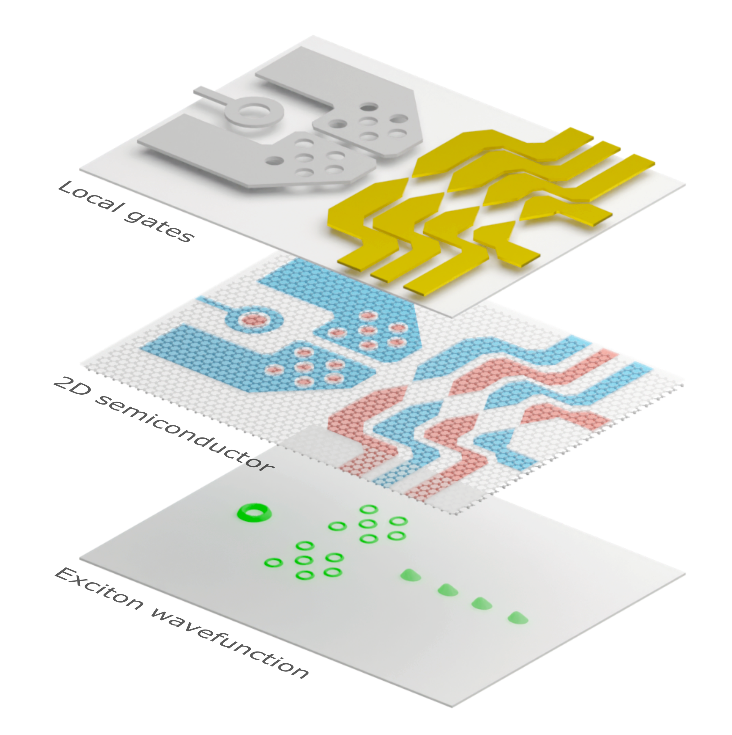
Quantum control of exciton wavefunctions in 2D semiconductors
Excitons –bound electron-hole pairs– play a central role in light-matter interaction phenomena, and are crucial for wide-ranging applications from light harvesting and generation to quantum information processing. A long-standing challenge in solid-state optics has been to achieve precise and scalable control over the quantum mechanical state of excitons in semiconductor heterostructures. Here, we demonstrate a technique for creating tailored and tunable potential landscapes for optically active excitons in 2D semiconductors that enables in-situ wavefunction shaping at the nanoscopic lengthscale. Using nanostructured gate electrodes, we create localized electrostatic traps for excitons in diverse geometries such as quantum dots and rings, and arrays thereof. We show independent spectral tuning of multiple spatially separated quantum dots, which allows us to bring them to degeneracy despite material disorder. Owing to the strong light-matter coupling of excitons in 2D semiconductors, we observe unambiguous signatures of confined exciton wavefunctions in optical reflection and photoluminescence measurements. Our work introduces a new approach to engineering exciton dynamics and interactions at the nanometer scale, with implications for novel optoelectronic devices, topological photonics, and many-body quantum nonlinear optics.
Introduction
The ability to trap and manipulate the quantum mechanical state of particles is a central pillar across various disciplines of quantum science, including ultracold atoms [1, 2], ion traps [3] and superconducting qubits [4]. In semiconductor optics, the traditional approach to confinement of optical excitations involves nanostructures such as self-assembled or colloidal quantum dots, which are typically fabricated through growth or implantation techniques. These methods lead to ensembles of quantum dots (or rings) with random positions and broad energy distribution with limited local control [5, 6, 7]. The resulting lack of scalability has hindered their widespread technological implementation. In addition to these methods, alternative material modulation approaches have recently been explored, such as strain engineering [8, 9, 10, 11, 12], electron and ion beam irradiation [13, 14], and moiré potential engineering [15, 16, 17, 18], which offer varying degrees of control on the positions, energies or number of emitters. Furthermore, electrostatic confinement of spatially indirect excitons in semiconductor heterostructures has been reported [19, 20]; however, their vanishing coupling to light limits potential photonics applications. The ability to precisely control the individual quantum states of optically active excitons with strong light-matter coupling has thus remained a major experimental challenge.
Recently, a novel technique has been reported for confining direct excitons purely using electric fields and charge density gradients in 2D semiconductor heterostructures [21]. The method relies on the fact that in-plane electric fields () induce a quadratic dc Stark shift of the excitons, and charge density () leads to an interaction-induced density-dependent energy shift, according to
| (1) |
where is the dc polarizability of excitons and is the exciton-electron coupling constant. Spatial variations of doping densities and electric fields can thus be used to trap excitons. Based on this effect, quantum confinement was demonstrated in a gate-defined lateral p-i-n junction. However, as the trapping occurs along the gate edges, the technique has so far been limited to excitonic 1D quantum wires.
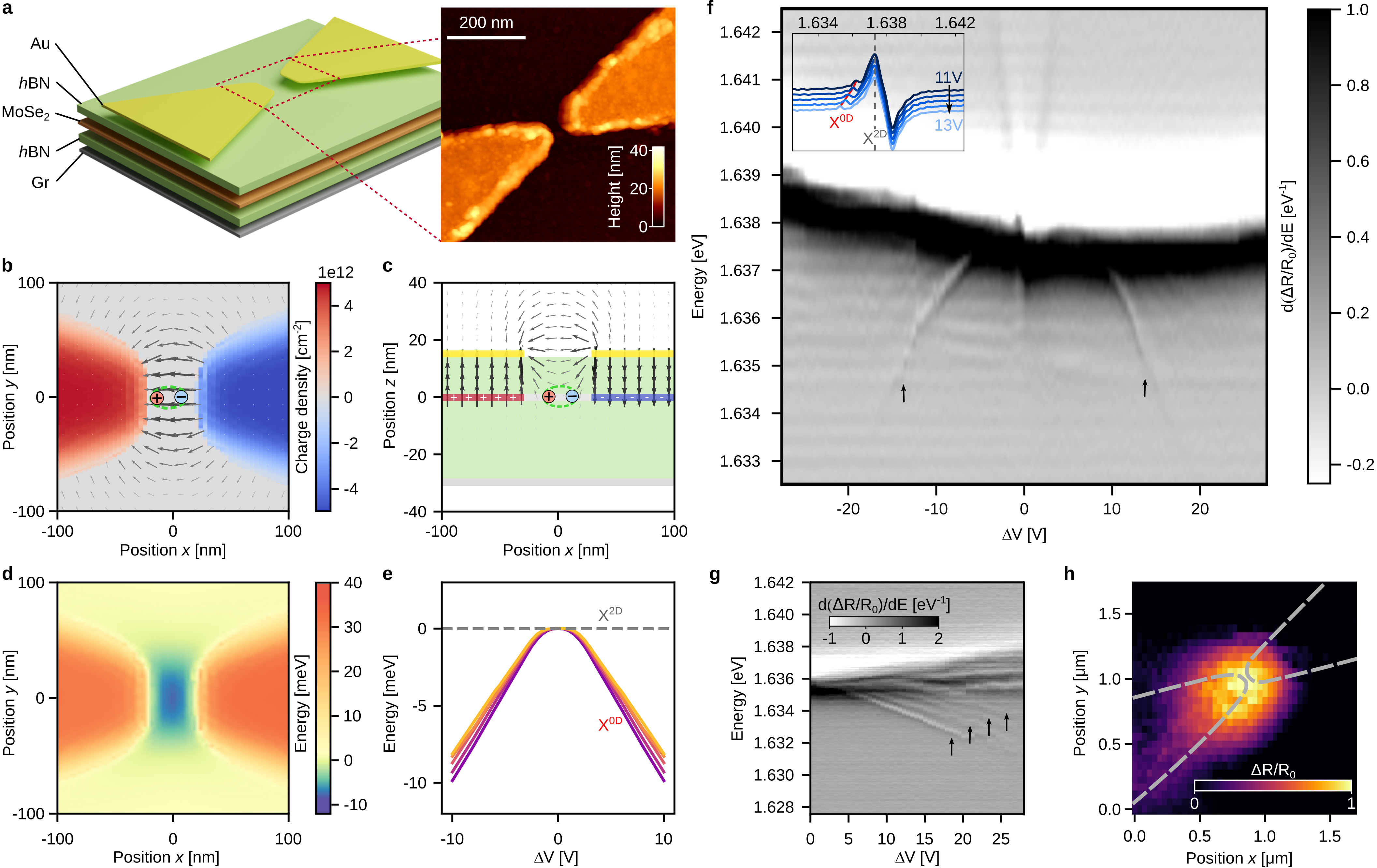
Here, we demonstrate scalable and tunable electrostatic traps of arbitrary shapes for direct excitons in monolayer Transition Metal Dichalcogenide (TMD) semiconductors. We illustrate our approach in Fig. 1. The crux of our work lies in using lithographically nano-structured gate electrodes in proximity to the 2D semiconductor plane (upper layer). This allows to precisely define the lateral distribution of in-plane electric fields and density of itinerant holes (red) and electrons (blue) in the 2D semiconductor, with a resolution down to a few tens of nanometers (middle layer). This in turn enables tailor-made landscapes for excitons with a high degree of control on the wavefunction profile (lower layer). To highlight the versatility of our technique, we focus on two exemplary trap geometries, namely quantum rings and quantum dots, that may serve as building blocks for more extended landscapes. Furthermore, we demonstrate the unprecedented scalability of our approach by realizing arrays of quantum rings and independently controlled quantum dots which is of particular relevance for future optoelectronics and photonics technologies.
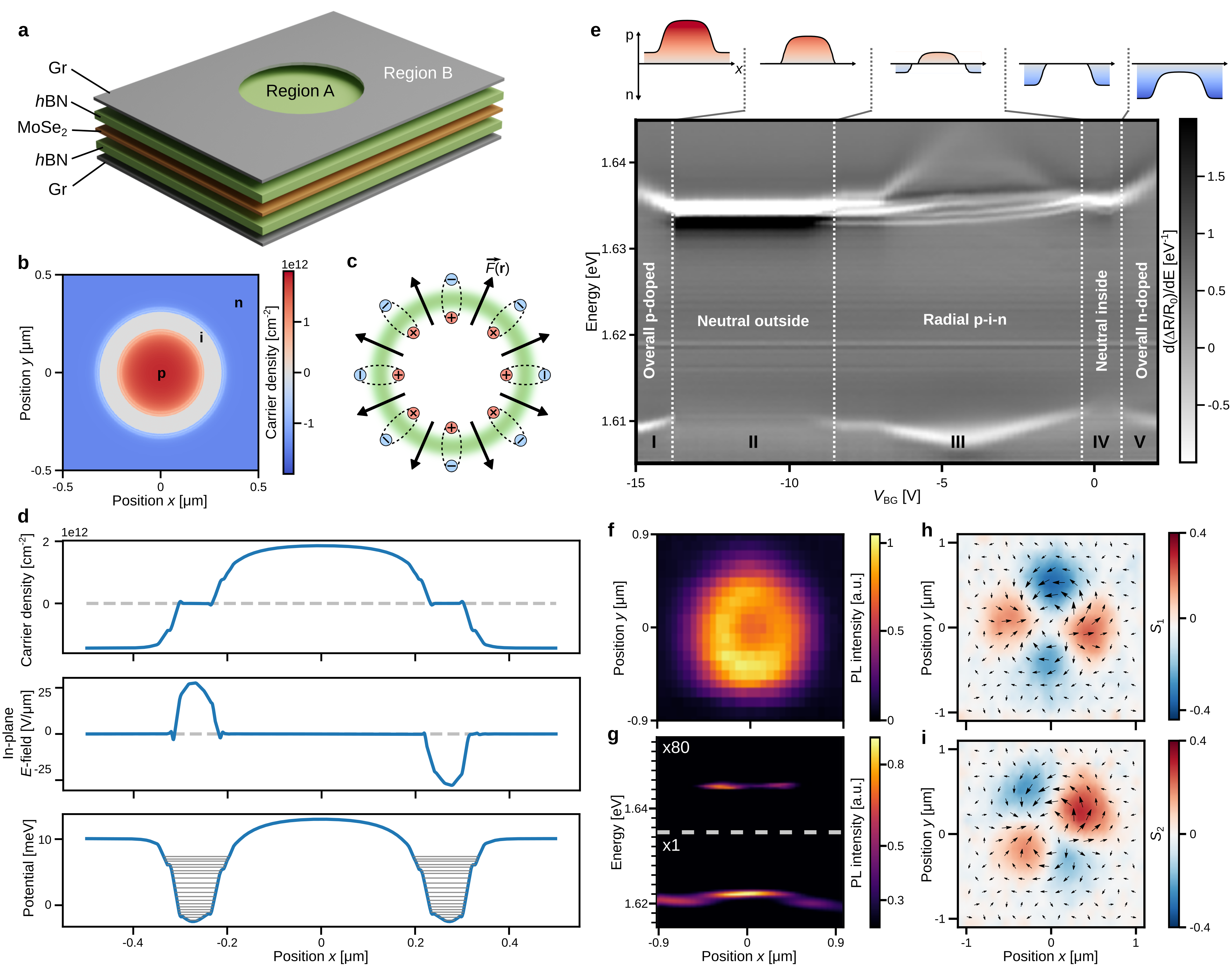
The basic structure of our exciton trapping devices consists of a monolayer TMD semiconductor, such as MoSe2, encapsulated by hexagonal boron nitride (hBN) spacers of appropriate thickness. This heterostructure is stacked on a Si/SiO2 substrate with top (TG) and bottom (BG) gate electrodes, which can either be graphene (Gr) or metallic thin films. We nanostructure one of the gate electrodes through a combination of electron beam lithography and dry etching, which allows for patterning resolutions of around 50 nm. A global BG is used to define the charge configuration of the entire monolayer, whereas the nanostructured TGs enable local control of charge densities and fields. Even though either of the gates can be patterned without losing functionality, we choose to define the structures on the TGs and keep the BG for global doping, for ease of fabrication. Our devices are cooled down to K in a closed cycle dry cryostat with optical access. To characterize the excitonic states in our system, we mainly rely on optical broadband reflection and photoluminescence spectroscopy with a spatial resolution of . A detailed account of our fabrication and experimental procedures is described in the Supplementary Information (SI .3,.1).
Excitonic quantum rings
In Fig. 2, we describe our scheme to create ring traps for excitons. An annular confinement geometry can be obtained simply by patterning circular holes in the TG, as shown schematically in Fig. 2 a. In order to obtain the strongest confinement, we apply opposite voltages on the top and bottom gates to reach the annular p-i-n regime, where a central p-doped puddle is enclosed in a Fermi sea of electrons with a ring-shaped neutral region separating them, as seen in Fig. 2 b. The combination of in-plane fields and charge gradients leads to tight confinement of excitons in this annular region (1). Furthermore, the in-plane fields lead to radially polarized in-plane dipolar excitons as illustrated in Fig. 2 c.
In Fig. 2 d, we show results of finite element simulations of the charge and field distributions in the annular p-i-n configuration for a top gate hole with diameter nm, which provides a quantitative understanding of the electrostatics of the device. We calculate the confinement potential according to Eq. 1, which shows the expected Mexican hat-like profile. We note that the dominant contribution to the potential comes from the exciton-electron interaction (second term in Eq. 1) whereas the Stark shift has a relatively mild effect. Solving the 2D Schrödinger equation in the center-of-mass (c.o.m) frame of excitons, we obtain discrete radial trap levels, with a level separation of meV. We present a detailed account of the trap profile as a function of voltage in the SI (section .6).
In order to verify the nature of excitonic states in this system, we now move on to optical measurements of the device. In monolayer MoSe2, the onset of electron or hole doping is associated with the emergence of a bound trion state and a density-dependent blue shifting exciton state (repulsive polaron) [22, 23, 24]. Therefore, measuring reflectance spectra as a function of and allows to precisely distinguish doping configurations inside and outside the TG hole. Region A (inside the hole) is primarily affected by the BG, whereas region B (outside the hole) can be doped using both TG and BG.
In Fig. 2 e, we present the measured reflectance spectra obtained from a nm diameter hole as a function of , for a fixed V. In order to highlight the faint signatures of quantum confined states, the reflectance contrast is differentiated with respect to energy as detailed in SI .2. Five distinct regimes can be identified as the applied back gate voltage is swept. For positive , the action of the back gate reinforces that of the top gate, leading to overall n-doping of the device (regime V in Fig. 2 e). As expected, we observe a trion branch at eV, and a repulsive polaron branch at eV. Decreasing reduces the electron density, until we reach the i-i-n regime where region A is neutral (regime IV), as evidenced by the transfer of oscillator strength from the trion branch to the neutral exciton state. As we decrease further, we reach the p-i-n regime where region A is p-doped and region B is n-doped (regime III), with an annular neutral region in between. Here, we observe repulsive polaron branches from both A and B regions, associated to the two types of carriers. In addition, we observe narrow and discrete resonances emerging from the neutral exciton state. We attribute these new resonances to 1D quantum ring states of different radial mode orders existing at the periphery of the nanohole. Upon decreasing the bottom gate voltage even further, the confined exciton states merge back with the 2D exciton continuum, as the region B outside the dot reaches charge neutrality (regime II). The energy separation between the discrete states is approximately meV, in agreement with the simulations, which corresponds to a trapping length of nm.
To investigate the spatial profile of the trap, we now turn to a larger TG hole of diameter m, which is large enough to optically resolve the different regions A and B with a confocal microscope setup. Fig. 2 f shows a spatially resolved photoluminescence (PL) map of the hole in the radial p-i-n configuration (V, V). The emission is filtered at the energy of the confined states. As expected, we observe a clear doughnut-shaped emission profile. The PL spectra taken along a cross-cut through the center of the hole (Fig. 2 g) shows distinct trionic emission from regions A and B, and confined states emission from the annular neutral region.
Further insights into the quantum ring states can be obtained by studying the polarization texture of the emitted photons. Previous studies on 1D confined states have shown that electron-hole exchange interactions, coupled with tight confinement of the excitonic wavefunction along one direction, leads to strong polarization splitting in a linear basis [21]. Applying this argument to our circular geometry, the ring confinement should induce polarization splitting in the radial-azimuthal basis. To investigate this behavior, we record the PL emission intensity from the lowest confined exciton as a function of position, for different polarization states (see SI .1). From these measurements, the normalized linear polarization Stokes vectors can be reconstructed as a function of position on the ring, where , , and respectively correspond to PL intensity along , , diagonal (), and anti-diagonal () directions, and is the total PL intensity. In Fig. 2 h and i, we show and for the lowest confined state which both exhibit two-fold symmetric patterns as expected for an azimuthally polarized emitter. These observations clearly demonstrate the quantum confinement of excitons in ring-shaped potentials, and constitute the first major result of this work.
Tunable quantum dots
We now turn to the demonstration of tunable quantum dot-like confinement, which has been a major goal in quantum photonics [25, 26, 27]. To generate electrostatic 0D nanotraps, we need a gate geometry that allows for tight confinement in both lateral directions. While the gate hole structure described in Fig. 2 may also be used for this purpose, the tightness of confinement and energy tunability is significantly limited by fabrication constraints. To achieve tunable 0D traps, we design a bow tie electrode structure as illustrated in Fig. 3 a, which concentrates electric fields in the nanoscopic gap between the electrodes. These bow ties are fabricated using electron beam lithography and deposition of nm Au, with gap sizes ranging from nm. An atomic force microscope micrograph of a bow tie ( nm gap) is shown in the inset.
In this geometry, we operate primarily in the neutral regime, where the semiconductor is globally set to neutrality using the bottom gate, and a bias voltage is applied between the bow tie electrodes to obtain in-plane fields in the nanogap. An electrostatic simulation of the charge and field distributions in the device is shown in Fig. 3 b and c (top and side view, respectively; red: holes, blue: electrons). In general, the top hBN thickness should be as small as possible (nm) in order to maximize the in-plane component of the electric field on the TMD plane in the gap region.
In Fig. 3 d, we show the expected 2D trapping potential for excitons in bow ties computed from Eq. 1. First, we note that in contrast to the ring traps, the dominant contribution to confinement in the bow tie geometry comes from the electric field-induced Stark shift (first term in Eq. 1). Further, the trapping potential features anisotropy, which can be adjusted by varying the width of the electrode tip and the gap size. By solving the 2D Schrödinger equation for the exciton c.o.m motion in such a potential, we obtain the expected dependence of the quantum confined states energies on , shown in Fig. 3 e.
To experimentally observe quantum dot states in the bow tie structure, we measure reflectance spectra in the gap region as a function of . These spectra are acquired from a bow tie with a gap size of nm. Since the gap size is much smaller than the diffraction limit, we expect that any confined states will have a strongly diminished oscillator strength as compared to the 2D exciton resonance. In Fig. 3 f, we show the first-derivative reflectance contrast spectra as a function of . For simplicity, we apply symmetric voltages on the two bow tie electrodes; eg. to obtain V, we apply V and V. In addition to the broad neutral 2D exciton background (centered around eV) and the blue-shifting polaron branches from the gated regions, we observe much narrower resonances emerging below the neutral exciton (linewidth eV). These states clearly red shift with , with a similar dependence to Fig. 3 e. This observed voltage dependence is in excellent quantitative agreement with our simulations (see SI .7). Line cuts at different are shown in the inset. The energy dependence of these states on the electric field across the bow tie is strong evidence that they occur in the gap region (see SI .7, .8). A further compelling signature of quantum confinement in such electrical traps is the emergence of a ladder of states corresponding to discrete energy levels in the trap [21]. In Fig. 3 f, such signatures are barely apparent possibly due to the small gap size leading to vanishing oscillator strength of excited states. To confirm this, we perform the same reflectance measurement on a bow tie with a larger gap size (nm), as shown in Fig. 3 g. Here we do observe a clear ladder of excitonic states emerging below the 2D exciton continuum, which supports our hypothesis.
To further confirm that the observed resonances indeed originate in the gap region, we perform a spatially resolved scan of reflectivity in the vicinity of the bow tie. For this measurement, a small voltage V is applied in order to further energetically separate the 0D state from the X2D background, which facilitates the analysis (see SI .8). The first-derivative reflectance contrast map, integrated over the narrow exciton resonance, is shown in Fig. 3 h which demonstrates that this resonance only appears close to the gap region and vanishes as we move away. We have reproduced these observations across different bow ties in the same device, as well as on several different devices (see SI .9), which underlines the robustness of our technique. Taken together, our measurements unambiguously demonstrate electrically tunable 0D quantum confinement in bow tie electrode structures, which constitutes the second key result of this work.
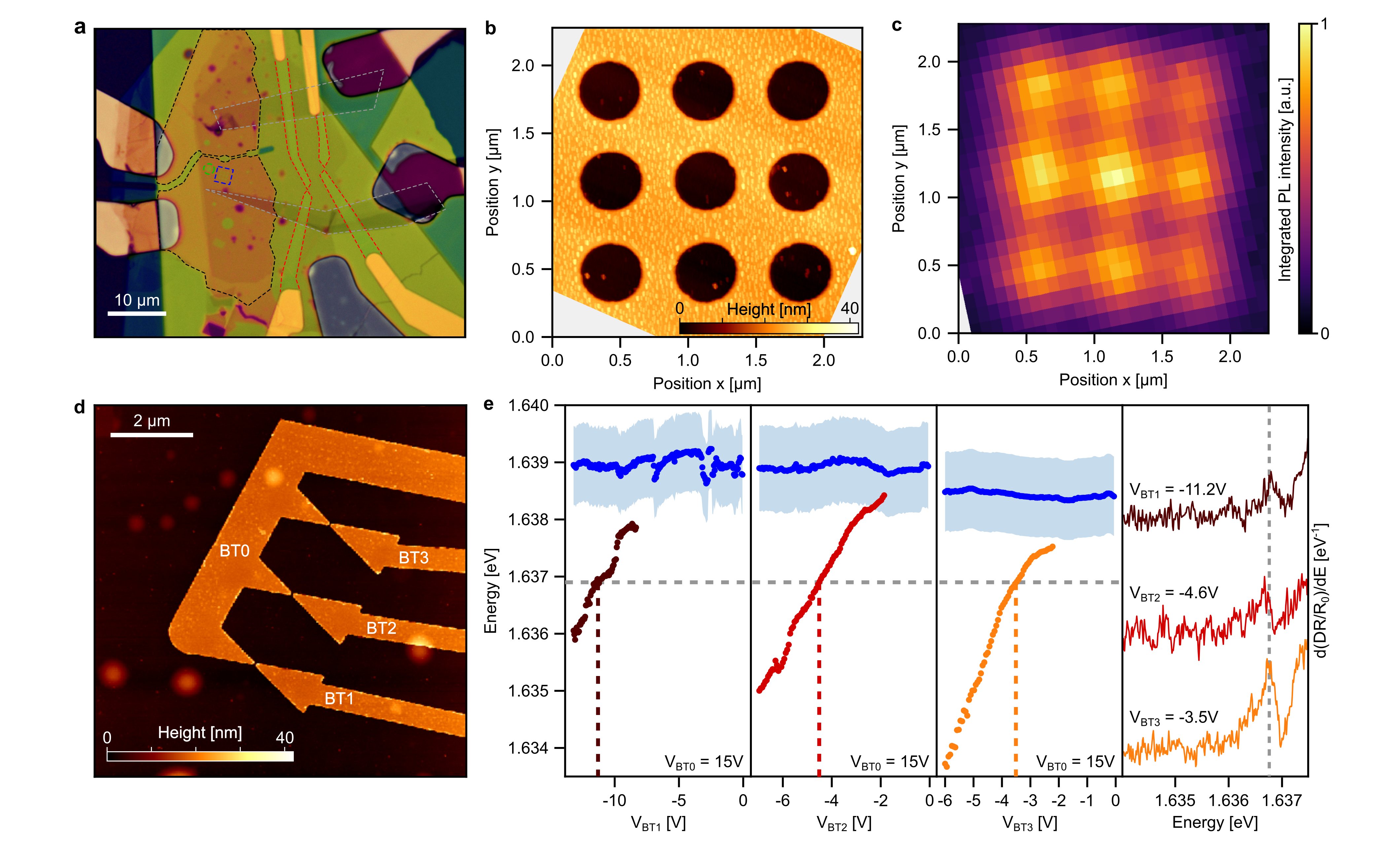
Scalable arrays of quantum dots and rings
The most important advantage of our approach for electrical nanoscale control of exciton wavefunctions is the potential for scaling up to more complex structures. The quantum dot and ring trapping schemes that we presented above can be seen as the building blocks for larger systems. Now, we demonstrate how a variety of nano-structures can be realized in a single TMD heterostructure simply by lithographically defining the desired gate patterns (Fig. 4). Figure 4 ashows a micrograph of a patterned heterostructure, demonstrating how different gate geometries can be defined on the same device. In Fig. 4 b, we show an AFM scan of a array of nm diameter holes, with a nm pitch that allows to optically resolve individual lattice sites. A spatially resolved scan of the PL emission, integrated over the quantum ring state resonances, is shown in Fig. 4 c. We clearly observe the emission profile of the ring array that matches excellently with the gate pattern. Since the hole diameters are smaller than the diffraction limit, we do not resolve the ring shape of the emission patterns (see Fig. 2 ffor comparison). This shows that ring traps can be scaled up arbitrarily in a single monolayer.
Next, we demonstrate the scalability of electrically tunable quantum dots. An important motivation for our work is the realization of multiple quantum dots with identical energies, which is a crucial and basic ingredient for several applications, including photonic quantum information processing and quantum communications [28]. This has so far remained a hurdle to achieve since existing material modulation approaches are drastically limited by material disorder and process variation [29]. We address this problem by fabricating an array of bow ties with independent control for each. An AFM scan of our structure with three bow ties with approximate gap size of nm and a separation of m is shown in Fig. 4 d. We electrically short the left-hand side electrodes of the three bow ties (BT0), while maintaining individual control on each of the right-hand side electrodes (BT1, BT2, BT3). This allows to reduce the number of control gates per quantum dot to only one, thus enhancing scalability without compromising on the control over each site. As shown in SI .9, we observe the quantum dot confinement signatures described in Fig. 3 f in each of the bow ties.
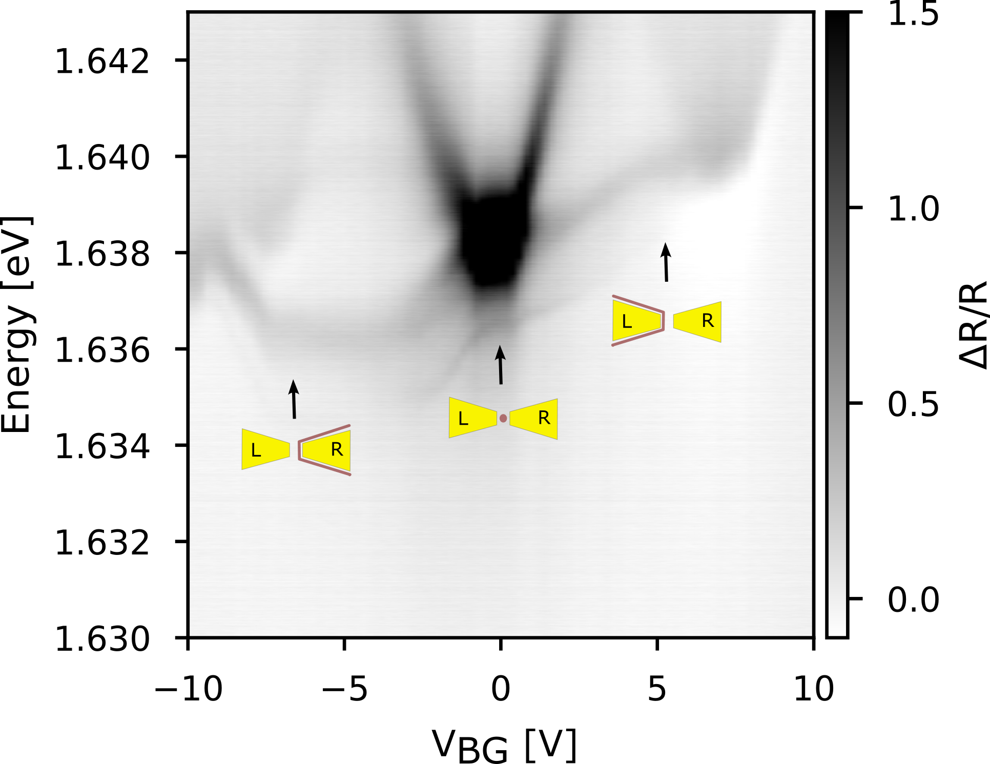
In Fig. 4 e, we report the fitted energy of the 0D states as a function of individual gate voltages , and , while keeping the common counter electrode at V. The energy of the 2D exciton is shown with blue dots and the linewidth is indicated by the blue shaded regions. The three bow ties show different dependence with voltage, possibly due to material disorder and variations due to fabrication uncertainties. Nevertheless, the three quantum dots can be simultaneously tuned to degeneracy (horizontal dashed line) by applying the suitable voltages across the bow ties (vertical dashed lines). This is clearly evident in the spectra shown in Fig. 4 f, taken at V, V, and V respectively, which show three quantum dot states resonantly tuned in energy. The ability to combine position-controlled lithographically defined quantum dots, with simultaneous and independent energy tunability into scalable arrays of quantum sites, constitutes the third main result of this work.
Outlook
We have demonstrated new fundamental building blocks for quantum excitonics. Our approach enables continuous control of the c.o.m wavefunctions, from micron sized extended states all the way down to quantum confinement into nanoscale dots and rings. Our approach is intrinsically scalable to independently tunable arrays, which is an important feature for future applications. A key advantage of this method is that arbitrary landscapes for excitons can be defined in a non-intrusive manner while retaining the pristine properties of the active material. Hence it can be extended to different semiconductors, including perovskites [30] and metal chalcogenide compounds [31]. Furthermore, improvements in fabrication techniques - in particular in lithography - will enable even smaller trapping length scales and better spatial control.
Our work opens up several avenues for further research. On the fundamental level, an important question is the nature of the confined excitonic state in the relative coordinates, which may be investigated by applying a combination of strong electric and magnetic fields [32]. Moreover, a detailed study of lifetime and coherence time will provide insights into exciton dynamics in such potentials. The fact that excitons confined in such nanoscopic traps still retain substantial oscillator strength is a major advantage, as this will enable strong coupling to light in microcavities [33] with expected Rabi splitting in the meV range. Arrays of such electrically confined quantum dots and rings may be combined with microcavity arrays to realize Bose-Hubbard model of photons [34]. The potentially enhanced optical nonlinearity of confined exciton systems may allow to go beyond the mean field regime and explore the strong correlations regime, where exotic phases such as Mott insulators are expected. Along the same lines, trapping radially dipolar excitons in ring potentials may have immediate relevance for effecting artificial gauge fields for optical excitations [35, 36], which is key to realizing topological effects such as a photonic fractional quantum Hall state. From the technological perspective, these configurable exciton landscapes could be of relevance for development of active photonic metamaterials [37] and novel light sources [38].
Acknowledgements. We are grateful to Patrick Knüppel, Deepankur Thureja and Andrea Bergschneider for fruitful discussions. We thank Deepankur Thureja for assistance with finite element simulations, and Elie Vandoolaeghe for help with the experimental setup. Funding: Support for the Stanford/SLAC researchers was provided primarily by the Q-NEXT Quantum Center, a U.S. Department of Energy (DOE), Office of Science, National Quantum Information Science Research Center, with additional support for device fabrication from the DOE, Office of Science, Office of Basic Energy Sciences (BES), Materials Sciences and Engineering Division and the Gordon and Betty Moore Foundation’s EPiQS Initiative through grant number GBMF9462. J.H. acknowledges support from NTT Research Fellowship. K.W. and T.T. acknowledge support from the JSPS KAKENHI (Grant Numbers 19H05790, 20H00354 and 21H05233).
Author contributions P.A.M. and T.C. conceptualized the work. J.H., X.C. and E.L. fabricated the devices. E.L., J.H. and T.C. performed the measurements and analysed the data. J.H. performed the simulations. P.A.M and T.C wrote the manuscript. K.W. and T.T. provided the hBN crystals. T.F.H., P.A.M and T.C. supervised the project.
References
- Gross and Bloch [2017] C. Gross and I. Bloch, Quantum simulations with ultracold atoms in optical lattices, Science 357, 995 (2017).
- Kaufman and Ni [2021] A. M. Kaufman and K.-K. Ni, Quantum science with optical tweezer arrays of ultracold atoms and molecules, Nature Physics 17, 1324 (2021).
- Bruzewicz et al. [2019] C. D. Bruzewicz, J. Chiaverini, R. McConnell, and J. M. Sage, Trapped-ion quantum computing: Progress and challenges, Applied Physics Reviews 6, 21314 (2019).
- Kjaergaard et al. [2020] M. Kjaergaard, M. E. Schwartz, J. Braumüller, P. Krantz, J. I.-J. Wang, S. Gustavsson, and W. D. Oliver, Superconducting Qubits: Current State of Play, Annual Review of Condensed Matter Physics 11, 369 (2020).
- de Arquer et al. [2021] F. P. G. de Arquer, D. V. Talapin, V. I. Klimov, Y. Arakawa, M. Bayer, and E. H. Sargent, Semiconductor quantum dots: Technological progress and future challenges, Science 373, eaaz8541 (2021).
- Aharonovich et al. [2016] I. Aharonovich, D. Englund, and M. Toth, Solid-state single-photon emitters, Nature photonics 10, 631 (2016).
- Azzam et al. [2021] S. I. Azzam, K. Parto, and G. Moody, Prospects and challenges of quantum emitters in 2d materials, Applied Physics Letters 118 (2021).
- Palacios-Berraquero et al. [2017] C. Palacios-Berraquero, D. M. Kara, A. R.-P. Montblanch, M. Barbone, P. Latawiec, D. Yoon, A. K. Ott, M. Loncar, A. C. Ferrari, and M. Atatüre, Large-scale quantum-emitter arrays in atomically thin semiconductors, Nature Communications 8, 15093 (2017).
- Rosenberger et al. [2019] M. R. Rosenberger, C. K. Dass, H.-J. Chuang, S. V. Sivaram, K. M. McCreary, J. R. Hendrickson, and B. T. Jonker, Quantum calligraphy: writing single-photon emitters in a two-dimensional materials platform, ACS nano 13, 904 (2019).
- Wang et al. [2021] Q. Wang, J. Maisch, F. Tang, D. Zhao, S. Yang, R. Joos, S. L. Portalupi, P. Michler, and J. H. Smet, Highly polarized single photons from strain-induced quasi-1D localized excitons in WSe2, Nano letters 21, 7175 (2021).
- Yu et al. [2021] L. Yu, M. Deng, J. L. Zhang, S. Borghardt, B. Kardynal, J. Vučković, and T. F. Heinz, Site-Controlled Quantum Emitters in Monolayer MoSe 2, Nano Letters 21, 2376 (2021).
- Lenferink et al. [2022] E. J. Lenferink, T. LaMountain, T. K. Stanev, E. Garvey, K. Watanabe, T. Taniguchi, and N. P. Stern, Tunable emission from localized excitons deterministically positioned in monolayer p–n junctions, ACS Photonics 9, 3067 (2022).
- Fournier et al. [2021] C. Fournier, S. R. Alexandre Plaud, A. Pierret, M. Rosticher, K. Watanabe, T. Taniguchi, S. Buil, X. Quélin, J. Barjon, J.-P. Hermier, and A. Delteil, Position-controlled quantum emitters with reproducible emission wavelength in hexagonal boron nitride, Nature Communications 12, 10.1038/s41467-021-24019-6 (2021).
- Gérard et al. [2023] D. Gérard, M. Rosticher, K. Watanabe, T. Taniguchi, J. Barjon, S. Buil, J.-P. Hermier, and A. Delteil, Top-down integration of a hbn quantum emitter in a monolithic photonic waveguide (2023), arXiv:2304.00130 [physics.optics] .
- Seyler et al. [2019] K. L. Seyler, P. Rivera, H. Yu, N. P. Wilson, E. L. Ray, D. G. Mandrus, J. Yan, W. Yao, and X. Xu, Signatures of moiré-trapped valley excitons in MoSe2/WSe2 heterobilayers, Nature 567, 66 (2019).
- Bai et al. [2020] Y. Bai, L. Zhou, J. Wang, W. Wu, L. J. McGilly, D. Halbertal, C. F. B. Lo, F. Liu, J. Ardelean, P. Rivera, N. R. Finney, X. C. Yang, D. N. Basov, W. Yao, X. Xu, J. Hone, A. N. Pasupathy, and X. Y. Zhu, Excitons in strain-induced one-dimensional moiré potentials at transition metal dichalcogenide heterojunctions, Nature Materials 19, 1068 (2020).
- Zhang et al. [2021] L. Zhang, F. Wu, S. Hou, Z. Zhang, Y.-H. Chou, K. Watanabe, T. Taniguchi, S. R. Forrest, and H. Deng, Van der waals heterostructure polaritons with moiré-induced nonlinearity, Nature 591, 61 (2021).
- Susarla et al. [2022] S. Susarla, M. H. Naik, D. D. Blach, J. Zipfel, T. Taniguchi, K. Watanabe, L. Huang, R. Ramesh, F. H. da Jornada, S. G. Louie, P. Ercius, and A. Raja, Hyperspectral imaging of exciton confinement within a moiré unit cell with a subnanometer electron probe, Science 378, 1235 (2022).
- High et al. [2009] A. A. High, A. K. Thomas, G. Grosso, M. Remeika, A. T. Hammack, A. D. Meyertholen, M. M. Fogler, L. V. Butov, M. Hanson, and A. C. Gossard, Trapping indirect excitons in a GaAs quantum-well structure with a diamond-shaped electrostatic trap, Physical Review Letters 103, 87403 (2009).
- Shanks et al. [2021] D. N. Shanks, F. Mahdikhanysarvejahany, C. Muccianti, A. Alfrey, M. R. Koehler, D. G. Mandrus, T. Taniguchi, K. Watanabe, H. Yu, B. J. LeRoy, and J. R. Schaibley, Nanoscale trapping of interlayer excitons in a 2d semiconductor heterostructure, Nano Letters 21, 5641 (2021), pMID: 34164985.
- Thureja et al. [2022] D. Thureja, A. Imamoglu, T. Smoleński, I. Amelio, A. Popert, T. Chervy, X. Lu, S. Liu, K. Barmak, K. Watanabe, T. Taniguchi, D. J. Norris, M. Kroner, and P. A. Murthy, Electrically tunable quantum confinement of neutral excitons, Nature 606, 10.1038/s41586-022-04634-z (2022).
- Sidler et al. [2017] M. Sidler, P. Back, O. Cotlet, A. Srivastava, T. Fink, M. Kroner, E. Demler, and A. Imamoglu, Fermi polaron-polaritons in charge-tunable atomically thin semiconductors, Nature Physics 3 (2017).
- Efimkin and MacDonald [2017] D. K. Efimkin and A. H. MacDonald, Many-body theory of trion absorption features in two-dimensional semiconductors, Physical Review B 95, 035417 (2017).
- Glazov [2020] M. M. Glazov, Optical properties of charged excitons in two-dimensional semiconductors, The Journal of Chemical Physics 153, 034703 (2020).
- Chen et al. [2014] L.-J. Chen, J.-D. Lin, and C.-R. Lee, An optically stable and tunable quantum dot nanocrystal-embedded cholesteric liquid crystal composite laser, J. Mater. Chem. C 2, 4388 (2014).
- Trotta and Rastelli [2015] R. Trotta and A. Rastelli, Engineering of Quantum Dot Photon Sources via Electro-elastic Fields BT - Engineering the Atom-Photon Interaction: Controlling Fundamental Processes with Photons, Atoms and Solids (Springer International Publishing, Cham, 2015) pp. 277–302.
- Wan et al. [2019] Y. Wan, S. Zhang, J. C. Norman, M. J. Kennedy, W. He, S. Liu, C. Xiang, C. Shang, J.-J. He, A. C. Gossard, and J. E. Bowers, Tunable quantum dot lasers grown directly on silicon, Optica 6, 1394 (2019).
- Gisin and Thew [2007] N. Gisin and R. Thew, Quantum communication, Nature Photonics 1, 165 (2007).
- Becher et al. [2023] C. Becher, W. Gao, S. Kar, C. D. Marciniak, T. Monz, J. G. Bartholomew, P. Goldner, H. Loh, E. Marcellina, K. E. J. Goh, T. S. Koh, B. Weber, Z. Mu, J.-Y. Tsai, Q. Yan, T. Huber-Loyola, S. Höfling, S. Gyger, S. Steinhauer, and V. Zwiller, 2023 roadmap for materials for quantum technologies, Materials for Quantum Technology 3, 12501 (2023).
- Wang et al. [2019] X.-D. Wang, W.-G. Li, J.-F. Liao, and D.-B. Kuang, Recent advances in halide perovskite single-crystal thin films: Fabrication methods and optoelectronic applications, Solar RRL 3, 1800294 (2019).
- Carey et al. [2017] B. J. Carey, J. Z. Ou, R. M. Clark, K. J. Berean, A. Zavabeti, A. S. Chesman, S. P. Russo, D. W. Lau, Z.-Q. Xu, Q. Bao, et al., Wafer-scale two-dimensional semiconductors from printed oxide skin of liquid metals, Nature communications 8, 14482 (2017).
- Fuhrer et al. [2002] A. Fuhrer, S. Lüscher, T. Ihn, T. Heinzel, K. Ensslin, W. Wegscheider, and M. Bichler, Energy spectra of quantum rings, Microelectronic Engineering 63, 47 (2002).
- Najer et al. [2019] D. Najer, I. Söllner, P. Sekatski, V. Dolique, M. C. Löbl, D. Riedel, R. Schott, S. Starosielec, S. R. Valentin, A. D. Wieck, N. Sangouard, A. Ludwig, and R. J. Warburton, A gated quantum dot strongly coupled to an optical microcavity, Nature 575, 622 (2019).
- Boulier et al. [2020] T. Boulier, M. J. Jacquet, A. Maître, G. Lerario, F. Claude, S. Pigeon, Q. Glorieux, A. Amo, J. Bloch, A. Bramati, and E. Giacobino, Microcavity polaritons for quantum simulation, Advanced Quantum Technologies 3, 2000052 (2020).
- Togan et al. [2018] E. Togan, H.-T. Lim, S. Faelt, W. Wegscheider, and A. Imamoglu, Enhanced Interactions between Dipolar Polaritons, Physical Review Letters 121, 227402 (2018).
- Chestnov et al. [2021] I. Y. Chestnov, S. M. Arakelian, and A. V. Kavokin, Giant synthetic gauge field for spinless microcavity polaritons in crossed electric and magnetic fields, New Journal of Physics 23, 023024 (2021).
- Takagahara [1992] T. Takagahara, Quantum dot lattice and enhanced excitonic optical nonlinearity, Surface Science 267, 310 (1992).
- Guzelturk et al. [2014] B. Guzelturk, P. L. H. Martinez, Q. Zhang, Q. Xiong, H. Sun, X. W. Sun, A. O. Govorov, and H. V. Demir, Excitonics of semiconductor quantum dots and wires for lighting and displays, Laser & Photonics Reviews 8, 73 (2014).
Supplementary Information
.1 Experimental setup
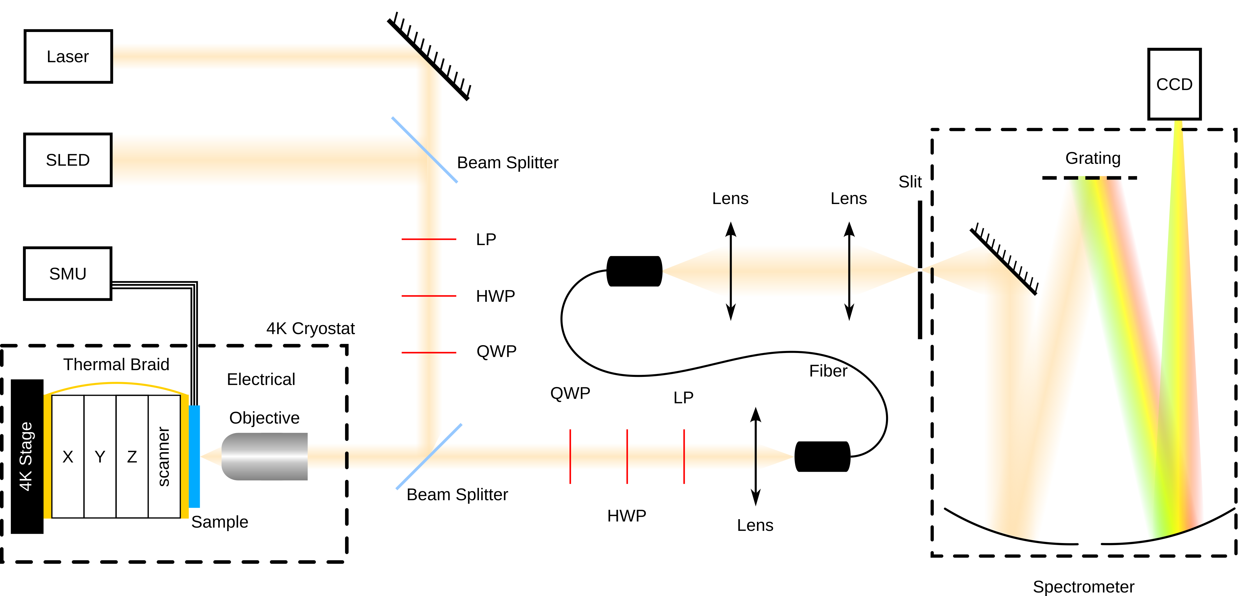
Figure S1 depicts our experimental setup. The sample is kept at K using an attoDRY800 closed-loop cryostat from Attocube. The sample is fixed on a custom made PCB board, which is mounted on a positioning piezo stack composed of three piezo stepper (two Attocube ANPx101/RES/LT and one ANPz102/RES/LT) and a piezo scanner (ANSxyz100std/LT). A cryo-, vacuum-compatible, high numerical aperture (NA = 0.81) objective (Attocube LT-APO/NIR/0.81) is used within the cryostat space. Voltages are applied to the sample gates using a Source Measure Unit (SMU) from Hewlett Packard (HP4142B) fitted with HP 41422B (41420A) modules.
The white light reflectivity measurements are performed using a Superluminescent Light Emitting Diode (SLED Exalos: EXS210065-01). A nm Ti:Sa continuous wave tunable laser (Matisse C from Spectra Physics), is used for photoluminescence measurement. The signal beam is collected through a single mode optical fiber (Thorlabs 630HP) that we use as a confocality pin hole. The corresponding collection area on the sample surface has a FWHM of m which sets the spatial resolution of our optical setup. The fiber output is directed to an imaging spectrometer (Andor SR-750-D1 with SR5-GRT-0600-0500, 600 line per mm grating) equipped with a Peltier cooled CCD camera (Andor DU940P-UV).
Polarization resolved experiments are performed using a set of broadband polarization optics in the excitation and detection arms, both consisting of linear polarizers (Thorlabs LPVIS100-MP2), half wave plates (Thorlabs AHWP10M-980), and quarter wave plates (Thorlabs AQWP10M-980). Linear Stokes vector maps are obtained by recording PL spectra in different linear polarization basis at each point on the sample:
where is the intensity of light polarized along () direction, and is the intensity of light polarized along the diagonal (antidiagonal) direction. is the total intensity of the signal.
AFM topographies are obtained in tapping mode, using ScanAsyst-air AFM probes on a MultiMode-8-HR AFM from Bruker.
.2 Differential reflectivity data analysis
Differential reflectivity spectra are obtained from the measured reflectivity by subtracting and dividing by the background spectrum , measured at the same spot with strong homogeneous doping. This is achieved by keeping the local top gates at 0 V and applying 10 V to the global back gate. Where needed, the differential reflectivity spectra are numerically differentiate with respect to energy () in order to increase the visibility of the confined states resonances.
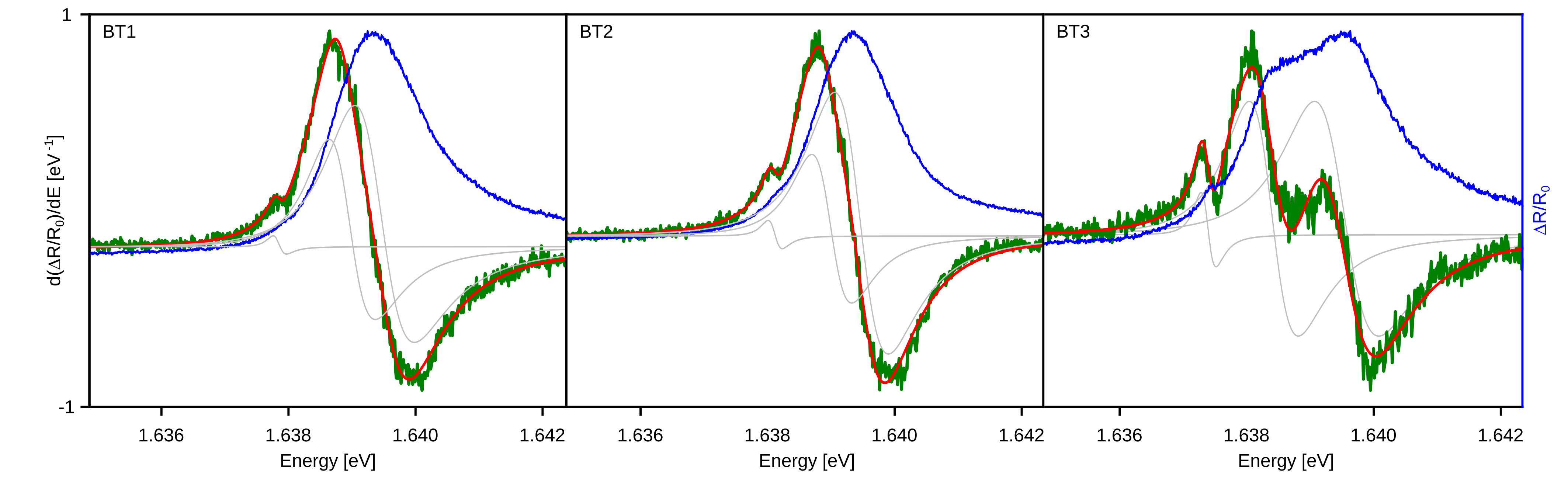
In Fig. 4 e, the energy of the 2D exciton and 0D exciton are shown. Those are extracted from fits of series. The reflectivity spectral lineshape () of heterostructures as studied here are well approximated by the sum of a pure and dispersive Lorentzian lineshapes ( and respectively), defined as follow:
with the Lorentzian amplitude, the Full Width at Half Maximum (FWHM), the central energy of the mode and the phase between the pure and dispersive Lorentzian. This Lorentzian is then numerically differentiate and fitted to the data, using the least_squares routine from the python library scipy.optimize.
The spectra present different features: the trapped exciton signal and a broad resonance for the 2D exciton. Three complex Lorentzian are used to fit the spectra, using the same phase parameter . Two Lorentzians are needed to fit the 2D exciton, most likely due to local strain in the TMD layer. Fig. S2 present an example of fit for the three different bow ties.
.3 Fabrication method
All hBN, graphite, and MoSe2 flakes used in this work are produced with mechanical exfoliation using scotch tape. The high-quality hBN crystal is from NIMS, and the MoSe2 crystal is from HQ graphene. The vdW heterostructure is assembled using the standard PC (polycarbonate) dry transfer method in an ambient environment. The heterostructure is then dropped down to a SiO2/Si substrate at 180 C. Multilayer graphite flakes are picked up as contacts to the MoSe2 monolayer.
Nanometer-scale features are generated with e-beam lithography (Raith Voyager, 50 keV) using a thin PMMA layer of 100 nm thick. For the quantum ring samples, the vdW heterostructure consists of hBN capping layer/top Gr gate/top hBN/MoSe2 monolayer/bottom hBN/bottom Gr gate. After e-beam patterning, the hBN capping layer and the graphite top gate are etched by reactive ion etching (Oxford Plasma Pro 80) sequentially. 10 sccm CHF3/10 sccm Ar/2 sccm O2 is used to etch hBN, and 10 sccm O2 is used to etch graphite. For the bow tie samples, the heterostructure consists of top hBN/MoSe2 monolayer/bottom hBN/bottom Gr gate. The same e-beam lithography process is used to pattern the nanogap, then a thin layer of metal (3 nm Ti/10 nm Au) is deposited as the top gates with a Kurt J. Lesker high vacuum e-beam evaporator.
The leads and bonding pads to the patterned gates and the sample contacts are formed by 5 nm Ti/45 nm Au, with patterns generated by either e-beam lithography (with 200 nm PMMA) or photo-lithography (ML3 MicroWriter).
The thicknesses of the top and bottom hBN of the devices discussed in the main text is listed in table S1.
.4 Electrostatic simulation method
The electrostatic simulation is done with COMSOL multiphysics electrostatic modeling on a 3D grid using finite element method. The TMD monolayer is modeled as a semiconductor, sandwiched in two insulating hBN slabs. The bottom gate is global and the top gate is set to be certain geometry. See ref.[21] for detailed parameters.
After the trapping potential is obtained from COMSOL simulation, the confined state energy and wavefunction is obtained by solving the 2D Schrodinger equation numerically in the c.o.m frame.
.5 Doping diagram
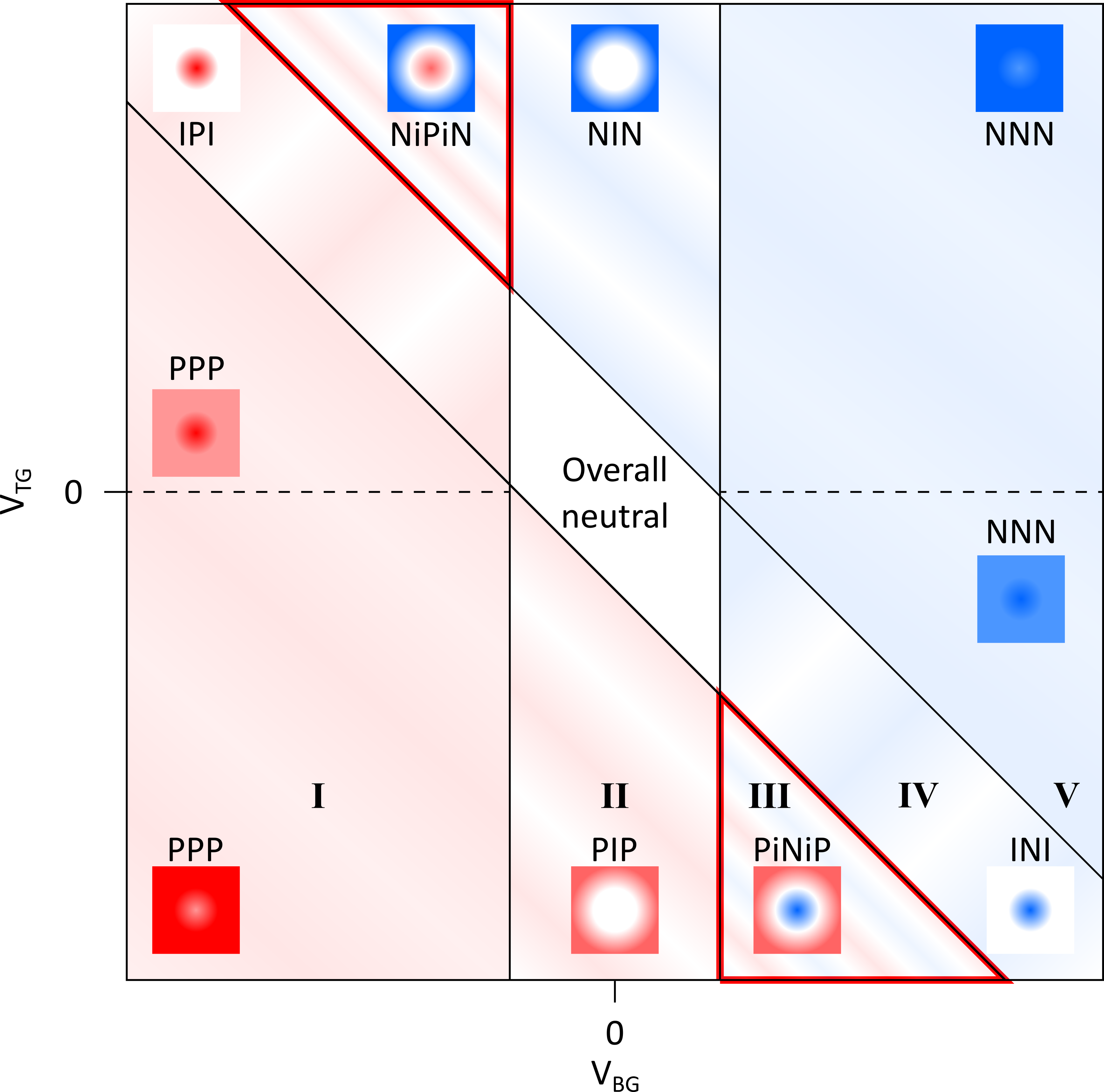
Fig. S3 presents a sketch of the top and bottom gate voltage dependence of the doping for a nanohole structure. First, the sample can be separated into two different region, the dual gated region outside the hole (region B in the main text), and the single gated region inside the hole (region A in the main text).
In region A, only the bottom gate acts to set the charge density of the TMD. Therefore, within the hole, the doping will switch from p- to n-doped due to the sole bottom gate. This result in the vertical lines on the doping diagram (Fig. S3), which are the bottom gate voltage at which the TMD switch from neutral to p- or n-doped.
The dual gated region however, one can tune separately the vertical electric field and the TMD doping. An opposite voltage between the top and bottom gate will result in an out of plane electric field and no doping, which is the central diagonal line of Fig. S3. On each side of this diagonal, p- and n-doped region of the outter hole appears.
Since the trapping of 1D edge states occurs in the p-i-n regions, the excitonic ring trap only appear in the upper left and bottom right red triangles (Fig. S3), where the doping in the hole is of a different kind than the doping outside it.
In addition, a weaker trap can be present in theory for the repulsive polaron, when both top gate and bottom gate are positive or negative. In this case, the inner part of the hole would be less doped, which will results in a lower energy polaron in the hole, and a higher one outside. The dashed line in Fig. S3 shows the limit at which the top gate voltage changes it sign which will induce a lower charge density outside of the hole and a larger one within. This latter configuration lead to an anti-trap for the repulsive polaron.
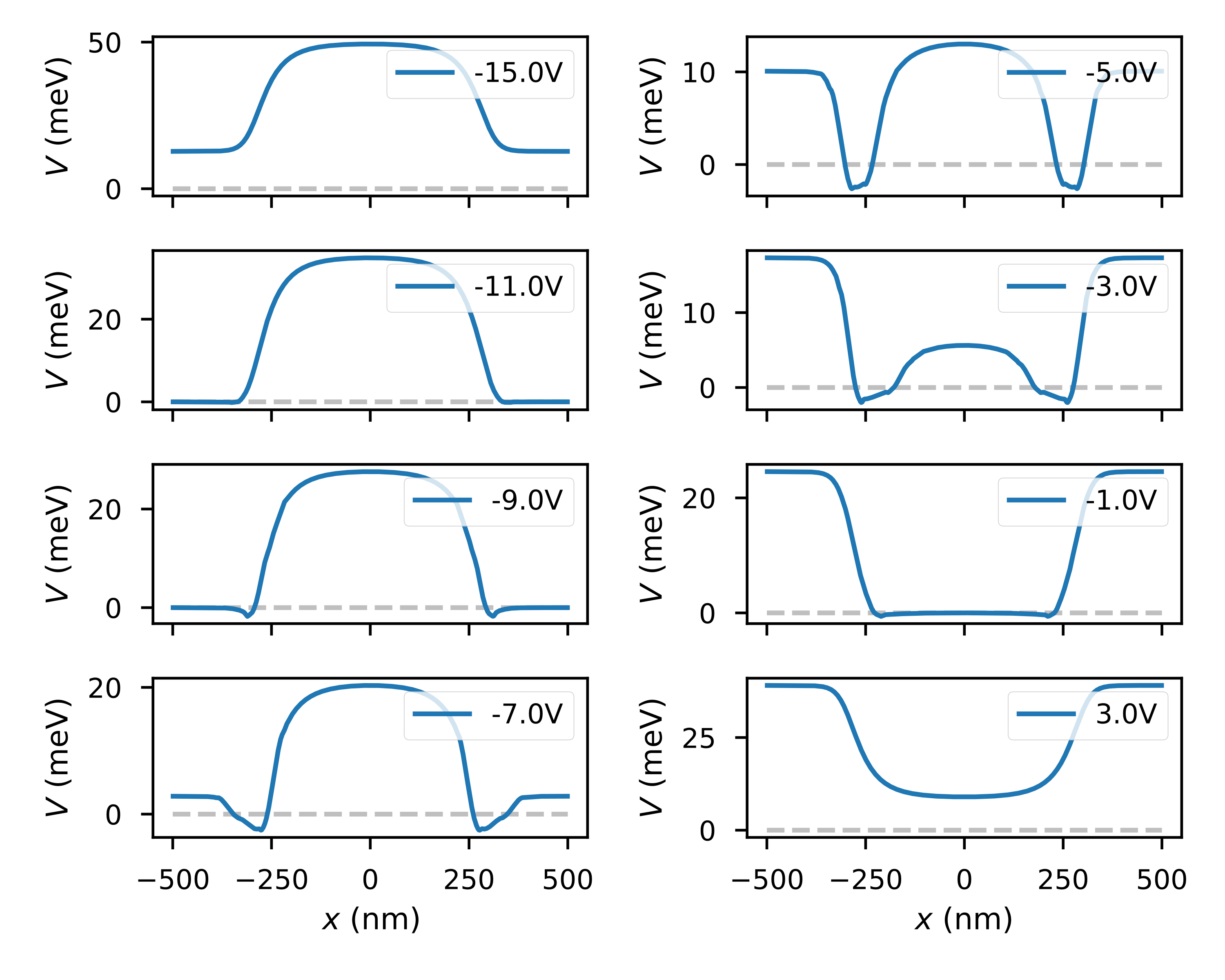
.6 Trapping potential vs in the 600 nm hole
Fig. S4 shows the simulated trapping potential at different in a 600 nm hole. Here is set to be V, the same as in Fig. 2 e. A ring-shaped trap is only formed when is from V to V, which agrees with our observation in Fig. 2 e that the trapped states only show up in regime III.
.7 Simulation results for tunable 0D states in the bow tie
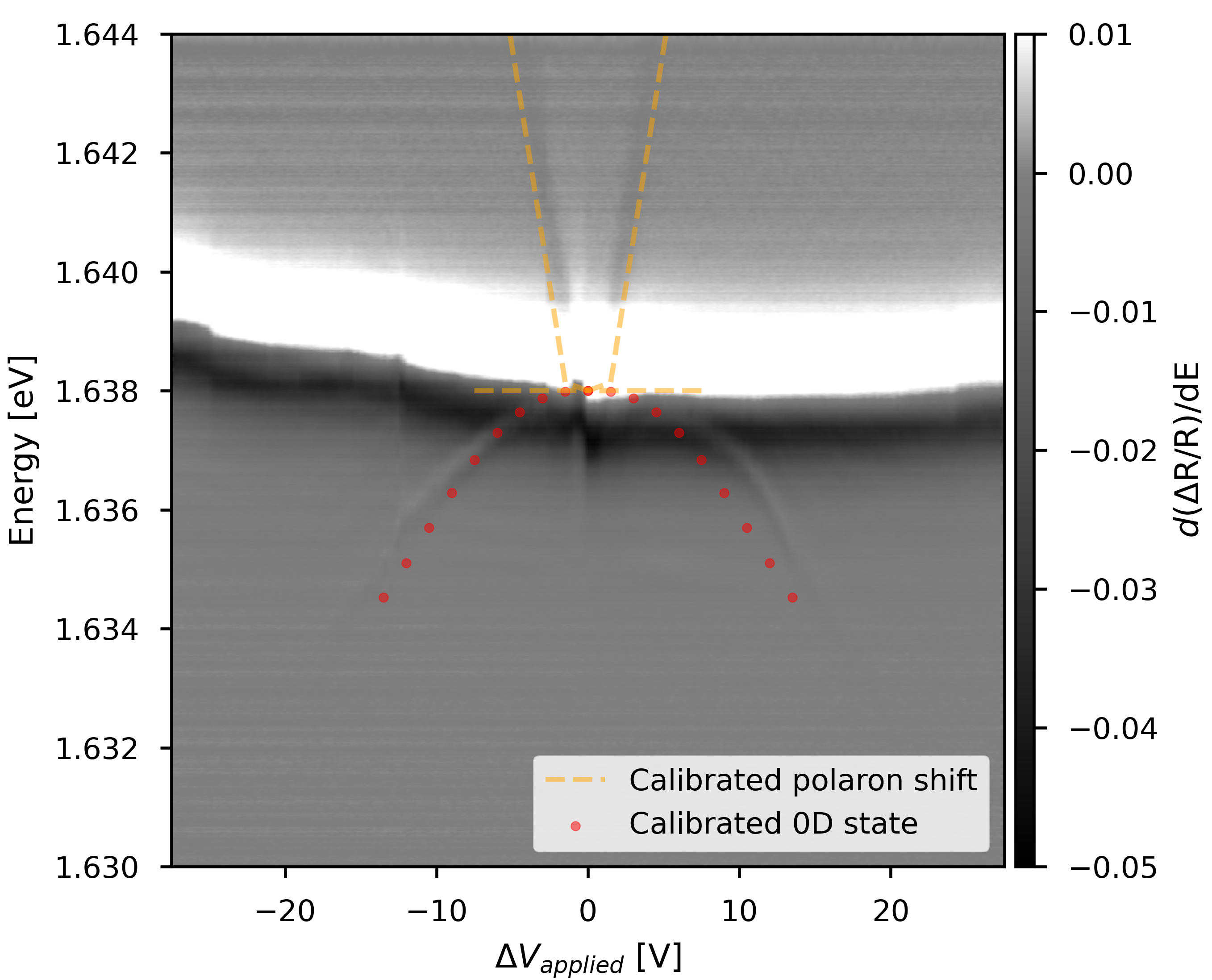
Electrostatic simulation for a nano-gap structure made with thin metal layers can be tricky. Due to the small size of the electrode and reduced conductivity, the voltage applied from the source-measurement unit might not reflect the actual voltage drop across the bow tie. This results in a much larger energy dispersion in the simulation compared to the measurements.
Here we present a way to calibrate the actual with respect to the applied . In the reflectivity spectra in Fig. 3 f, we observe both the 0D states and the blue-shifting repulsive polaron (RP) emerging from charging the TMD below the left and right electrodes. The blueshift of the RP corresponds to the second term in Eq.1, which can be calculated from the simulated charge density. By comparing it to the measured RP blueshift, we determine a reduction factor that overlaps the simulated polaron shift to the measured polaron shift, as shown in Fig. S5 (here ). Then we use the same reduction factor to calculate the trapping potential and solve the energy dispersion of the 0D states (shown in red dots in Fig. S5). It agrees reasonably well with the measurement.
.8 Transition from 0D confinement to 1D confinement in the bow tie
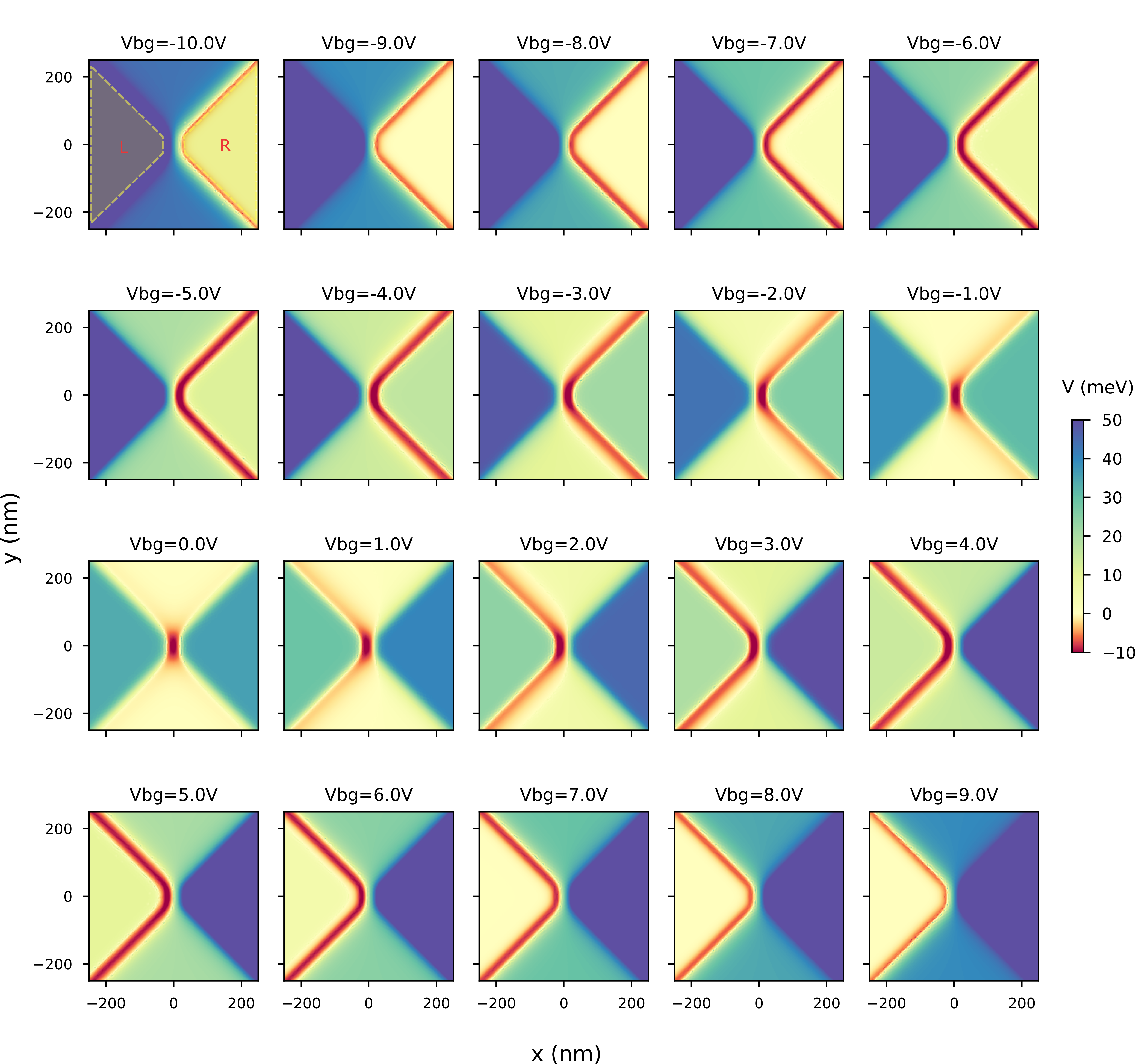
Here in Fig. S6, we show the simulation results for the potential landscape in the bow tie structure, as a function of the backgate voltage. The left and right bow tie electrodes are at +5 V and -5 V respectively, i.e. V. It demonstrates a continuous transition from the 0D dot confinement (V) to 1D edge confinement wrapped around the right (left) electrode when is tuned to negative (positive) values. This 0D to 1D transition is observed experimentally as well, see Fig. S7.
Fig. S8 shows a dual gate reflection contrast scan at V. Panel a is the integrated reflection map, and the vertical (horizontal) stripe shows the gates range where the 2D exciton under the right (left) bow tie electrode is kept neutral. Panel b is the line cut along the solid line in panel a which corresponds to applying across the bow tie. As expected, signature for 0D trapped states is present. Panel c is the line cut along the dashed line in panel a, corresponding to V. No 0D state is observed because no trap is formed when the same voltage is applied to both bow tie electrodes.
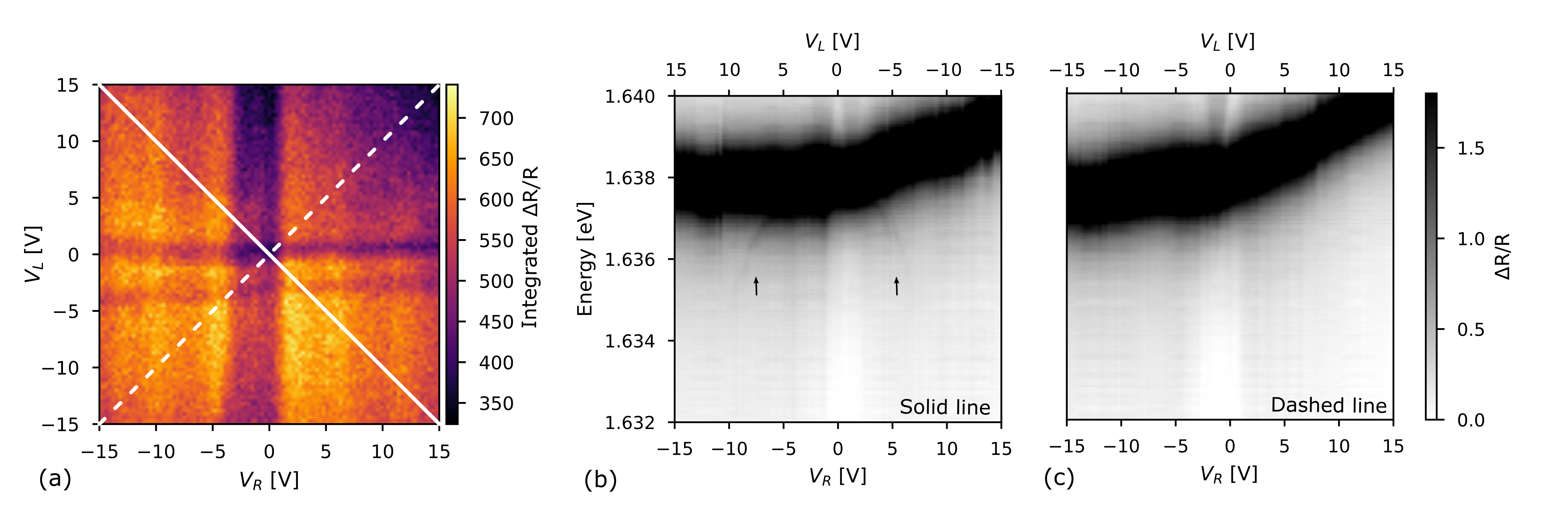
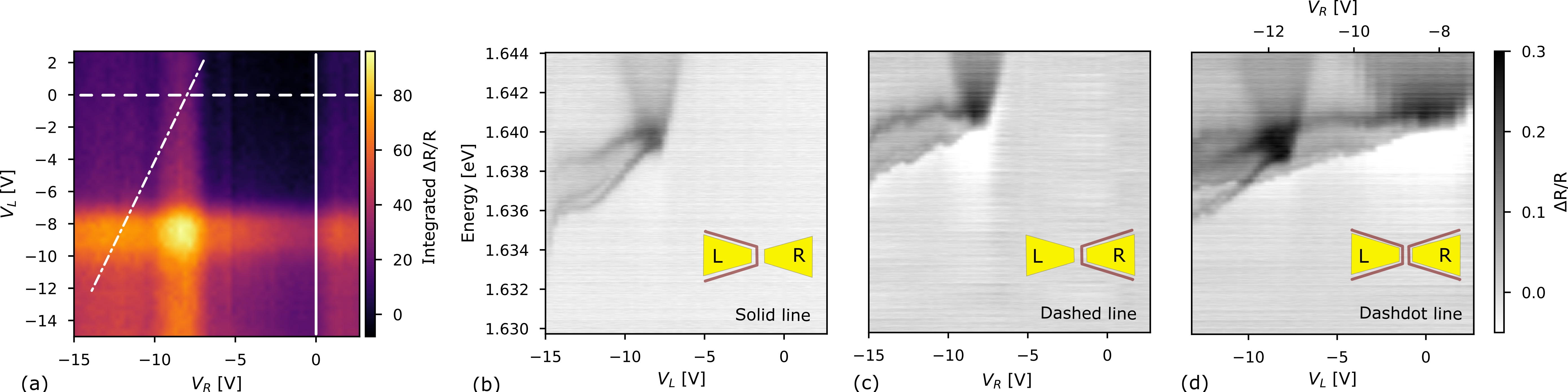
Fig. S9 shows a dual gate scan map of reflectivity at V. Panel a is the integrated reflection map, and the vertical (horizontal) stripe indicates the gates range where the 2D exciton under the right (left) bow tie electrode is tuned to neutrality. This is at a negative voltage now because is set to be positive. Panel b is the line cut along the solid line at V, showing 1D confined states around the left bow tie electrode (as shown in the inset). Panel c is the line cut along the dashed line at V, showing 1D confined states around the right bow tie electrode. Panel d plots the line cut along the dashdot line, displaying two groups of 1D confined states around both bow tie electrodes. The two sets of 1D confined states can also be tuned to resonance. This shows that bow tie structures are very versatile and can host both 0D and 1D tunable confined exciton.
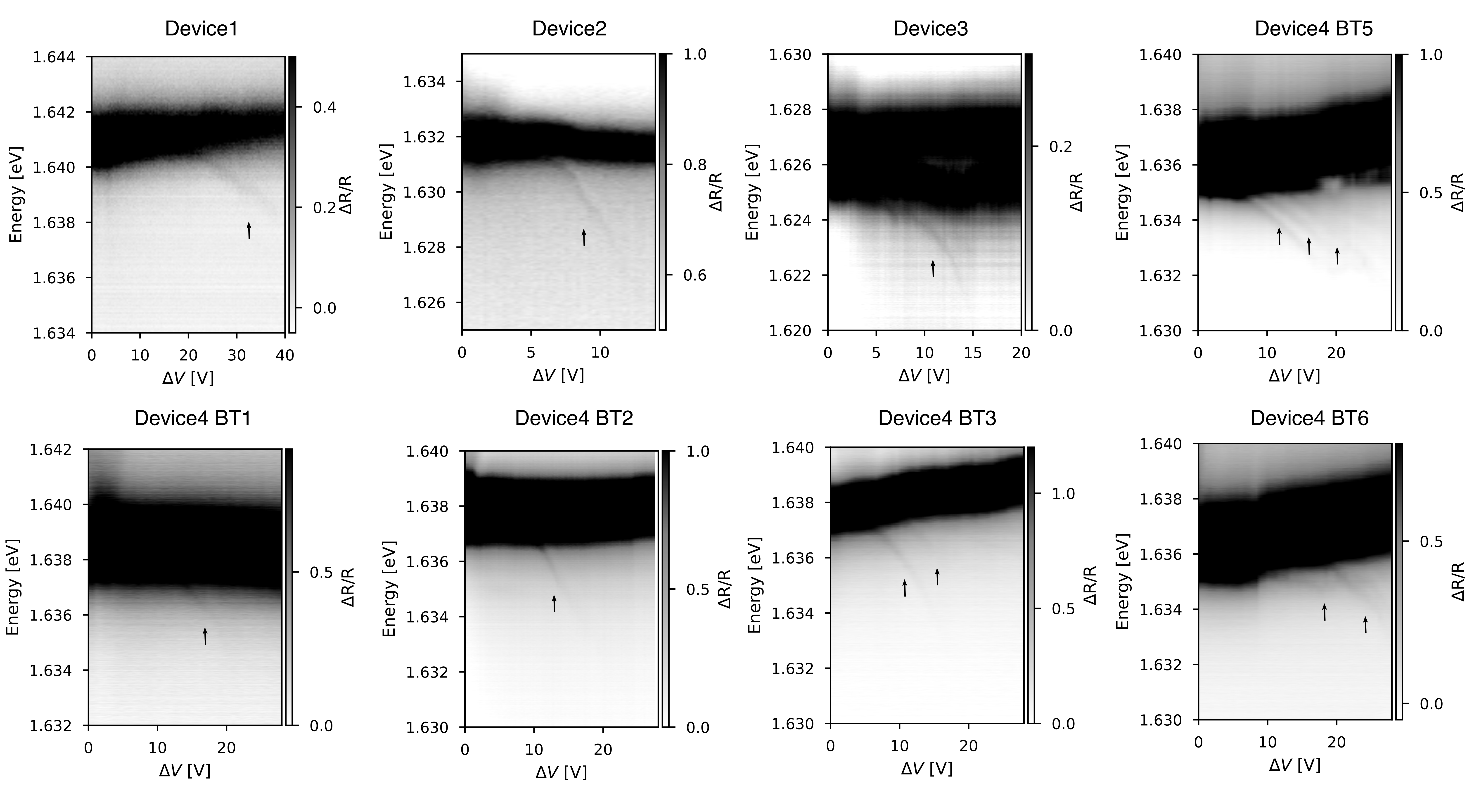
.9 0D trapped states in multiple samples
The 0D trapped state is consistently observed in various bow tie structures on multiple samples, as shown in Fig. S11. For some bow ties, we only see 0D state on one side of , possibly due to charge inhomogeneity around the nano-gap region.
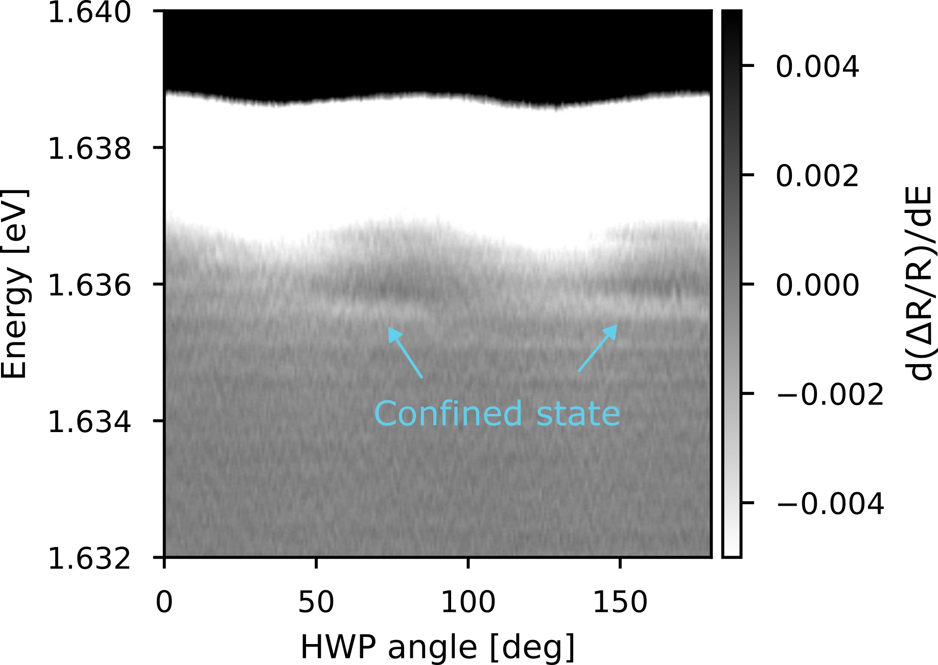
.10 Polarization dependence of the 0D states
In Fig. S10, we show the polarization dependence of the 0D trapped states in the bow tie structure. The trapped state follows a linear polarization basis, consistent with the anisotropy of the trapping potential shown in Fig. 3 d.