Interpretable inverse-designed cavity for on-chip nonlinear and quantum optics
Abstract
Inverse design is a powerful tool in wave-physics and in particular in photonics for compact, high-performance devices. To date, applications have mostly been limited to linear systems and it has rarely been investigated or demonstrated in the nonlinear regime. In addition, the "black box" nature of inverse design techniques has hindered the understanding of optimized inverse-designed structures. We propose an inverse design method with interpretable results to enhance the efficiency of on-chip photon generation rate through nonlinear processes by controlling the effective phase-matching conditions. We fabricate and characterize a compact, inverse-designed device using a silicon-on-insulator platform that allows a spontaneous four-wave mixing process to generate photon pairs at 1.1MHz with a coincidence to accidental ratio of 162. Our design method accounts for fabrication constraints and can be used for scalable quantum light sources in large-scale communication and computing applications.
I Introduction
Enhancing nonlinear optical processes has been a long-standing challenge due to materials’ weak nonlinear response. The quest for effective approaches to achieve on-chip frequency conversion and generate photon pairs has been an enduring endeavor. Over the last decades, various nanophotonic platforms have been proposed to implement and enhance nonlinear photon generation processes, including wire waveguides 1; 2, nanobeam cavities 3, metamaterials 4, microring resonators5; 6; 7; 8; 9; 10; 11; 12; 13; 14; 15; 16, periodically poled waveguides/cavities17; 18, and photonic crystal cavities19; 20; 21. It is well-known that high-quality factor cavities designed at target frequencies can bolster the nonlinear process by enhancing the field with confinement. Yet, the effective phase matching conditions are typically challenging to satisfy in non-conventional cavity structures. Without effective phase-matching, the generated photons from different positions in nonlinear materials can destructively interfere, reducing the total generation efficiency. Such issues can be addressed by computational inverse design 22; 23; 24; 25; 26; 27; 28; 29. Recently, the adjoint method has been generalized to optimize nonlinear photonic processes, such as second harmonic generation or optical switches based on the Kerr effect 30; 31; 32; 33. However, current optimization methods face difficulties in generalization to multi-photon generation processes, and the coupling efficiencies for both input and output channels are often overlooked due to the optimization complexity. In addition, an intuitive understanding of the inverse-designed structure is unclear. The optimized structure often lacks interpretability, making it challenging to gain insights into how and why the inverse design method works.
To address these challenges, we put forth an inverse design approach to amplify the efficiency of on-chip photon pair generation. We implement this strategy using the open-source package EmOpt 34. Our method employs a multi-frequency co-optimization strategy and calculates gradients with respect to the design parameters via the adjoint method. The resulting efficiency enhancement stems not only from the increased field intensity due to the confinement of light in high quality factor cavity resonances but also from the improvement of phase-matching conditions, along with coupling between the cavity and waveguide mode considered in the design. We demonstrate the capability of the proposed method by fabricating and characterizing an optimized device that enables the efficient generation of photon pairs. Interestingly, the shape of the proposed design can also be explained by an effective potential method, and the approximate solution aligns well with the finite-difference frequency domain (FDFD) simulation results. The proposed optimization strategy can be generalized to other nonlinear processes for compact frequency-mixing devices on-chip, and the performance can be further improved using global optimization methods 35; 36.
II Method and proposed device
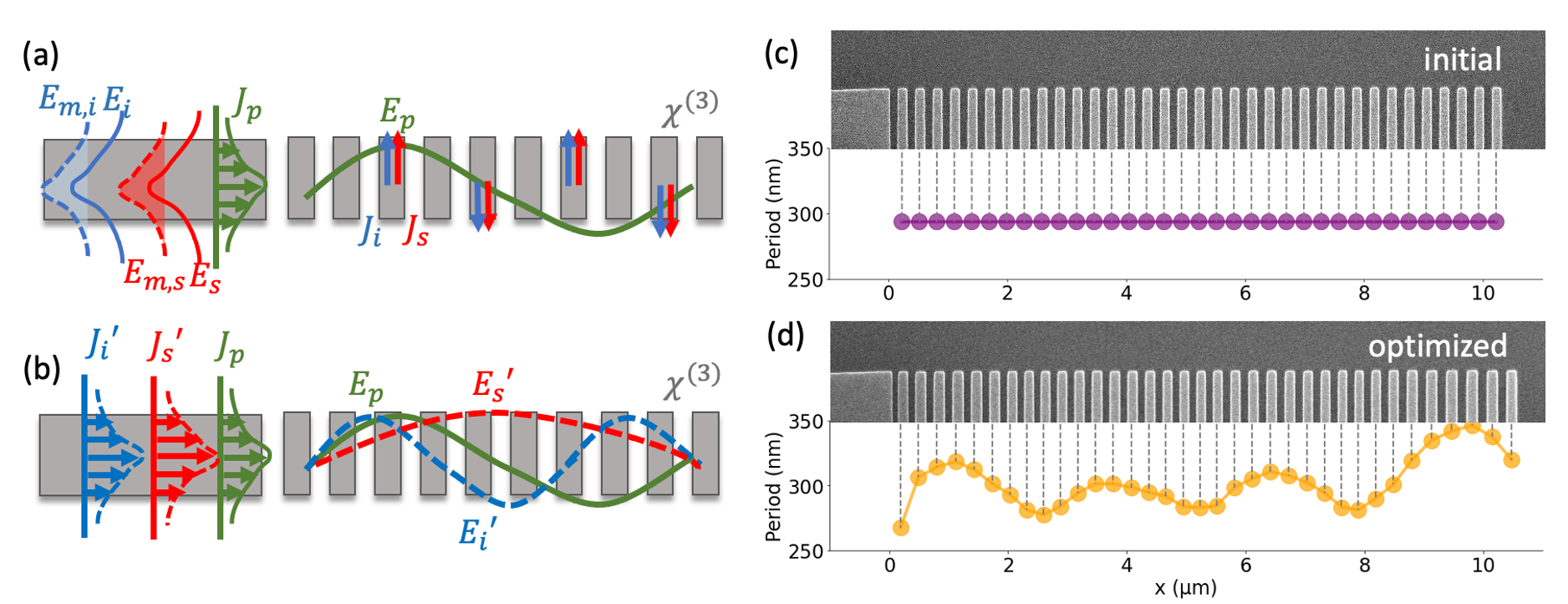
The proposed multi-frequency co-optimization method exemplifies the spontaneous four-wave mixing process shown in Fig. 1(a), where a single port is used to couple the pump/generated photons to/from the cavity. In the forward process, the fundamental mode at frequency is injected from the waveguide into the cavity, exciting the electric field distribution noted as in Fig. 1(a). Owing to the presence of the nonlinearity, vacuum fluctuations create dipole sources at other frequencies, specifically, signal and idler, shown as and . The generated photons in the spontaneous four-wave mixing process are designed to be collected back to the same waveguide. The collection efficiency can be represented as a mode-matching integral between the collective radiation field generated by dipoles and the waveguide mode at signal and idler frequencies . Such nonlinear photon pair generation process can be approximated by the adjoint process shown in Fig. 1(b), where the adjoint sources , i.e., the fundamental mode of the waveguide at signal and idler frequencies and , are reversely propagated back into the cavity. The efficiency can be represented in terms of the effective phase-matching integral as:
| (1) |
where is the effective phase-matching integrand, is the third-order nonlinear coefficient of the material, is the field distribution at pump frequency, while and are adjoint fields at signal and idler frequencies under continuous-wave (CW) excitation from the coupling waveguide. The integral is carried out over the cavity region.
The proposed figure of merit can be interpreted as follows. First, the pump, signal, and idler frequencies () in Eq. (1) can be selected in the CW-simulation to satisfy the energy conservation . Second, the figure of merit uses the non-normalized electric fields (), each obtained from a source excitation with fixed amplitude. The non-normalized field captures the cavity enhancement of the field intensities at the three frequencies, which also includes the coupling between the waveguide and the cavity for an efficient collection of the generated photons. In addition, with the overlap integral, the in-cavity phase-matching will be satisfied after the optimization to ensure the constructive interference of the generated photons.
III Optimization results
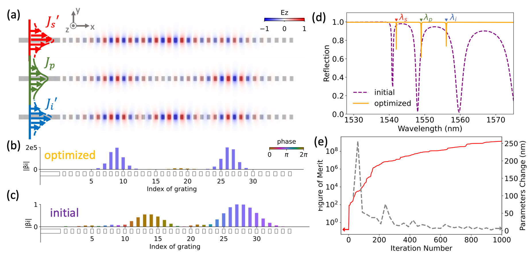
We adopt the hierarchical inverse design strategy, a two-step approach that proposes an initial physics-based guess, followed by a shape optimization using the adjoint method 37. Such strategy minimizes the computational cost by avoiding the large number of random guesses for initial conditions, and the fabrication limits can be easily enforced by adding simple shape constraints. Here, we perform the optimization using the width and gap of each grating, and the initial design is a periodic grating structure shown in Fig. 1(c) with the number of gratings , width and gap as . The optimized grating structure is shown in Fig. 1(d) with three energy-matching resonant modes shown in Fig. 2(a). During the optimization, the fundamental TE mode is injected into the waveguide at the pump wavelength , and the field distribution is computed by the 2D FDFD solver of EMopt. The fundamental modes at signal and idler frequencies () are excited by adjoint source (), also injected from the waveguide, at and , respectively. The cavity enhancement of the fields can be visualized from the contrast of the field inside the cavity compared to that in the incident waveguide. The phase-matching integrand in Eq. (1) is visualized as the bar plot in Fig. 2 (b) and (c) for each grating. The heights of the bars stand for the amplitudes and the color for the phases. The field enhancement of five orders of magnitude is shown on the normalization of the y-axis after optimization. In the ideal case where all grating pitches are excited and contribute constructively to the photon generation, the phase (i.e., color) should be identical. Compared with the phase-matching plot for the initial period grating in Fig. 2(c), the phase-matching condition is greatly enhanced as the phase difference is minimized. The resonant frequencies of the modes can be probed as minima in the reflection spectrum, shown in Fig. 2(d). Initially, the resonances are not equally spaced, the quality factors are not high enough, and the phase-matching condition is not satisfied. After optimization, the three resonances are equally spaced in frequency, with sharper peaks in reflection due to the improved quality factors. The optimization uses the limited-memory BFGS (L-BFGS) algorithm 38 with hard constraints on the minimum width and gap to be larger than . The convergence of parameters can be observed from Fig. 2(e), with negligible parameters’ change after approximately 600 iterations, and the increment of the figure of merit is also shown.
IV Measurement results
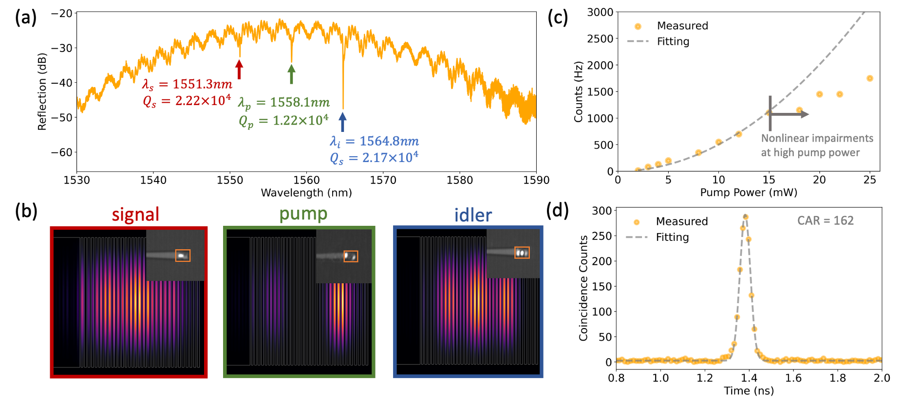
As an experimental demonstration, we use conventional silicon on insulator (SOI) wafer with silicon layer with oxide box layer below. The device requires a single e-beam lithography and etching process followed by adding an oxide cladding of um. We choose the transverse length of for simplicity in fabrication. The reflection spectrum of the inverse-designed device is measured by an optical spectrum analyzer in the linear regime, and the minima in reflection are extracted and fitted to obtain the loaded quality factor of pump, signal, and idler frequencies [Fig. 3(a)]. To confirm the field profile, the device is excited at resonance frequencies from a continuous wave laser source, and the scattered light is captured with an infrared camera as shown in Fig. 3(b). The obtained image is compared with the simulation, where the field is monitored above the device plane with Fourier components collected within the numerical aperture of the objective lens (). The agreement between simulation and experiment confirms that the field distributions are optimized for phase-matching. Next, the nonlinear experiment characterizes the paired photon generation efficiency. The CW-laser is tuned to the pump wavelength, and the output power at signal frequency is monitored at different input power levels, shown in Fig. 3(c). The output power is proportional to the pump power squared, as expected for a degenerated spontaneous process before other nonlinear effects, such as free carrier or two-photon absorption, show up at around mW 39. The quantum nature of photon-pair is confirmed by the intensity correlation measurement in Fig. 3(d), where the peak in the correlation indicates the photon pairs are generated simultaneously. The coincidence to accidental ratio is obtained from the fitted Gaussian curve as 162 and a maximum on-chip generation rate is at an on-chip pump power after compensating for the loss. In the experiment, the signal and idler photons are filtered out with cascaded narrowband tunable filters, with extinction ratio for each channel.
V Interpretation of inverse-designed device
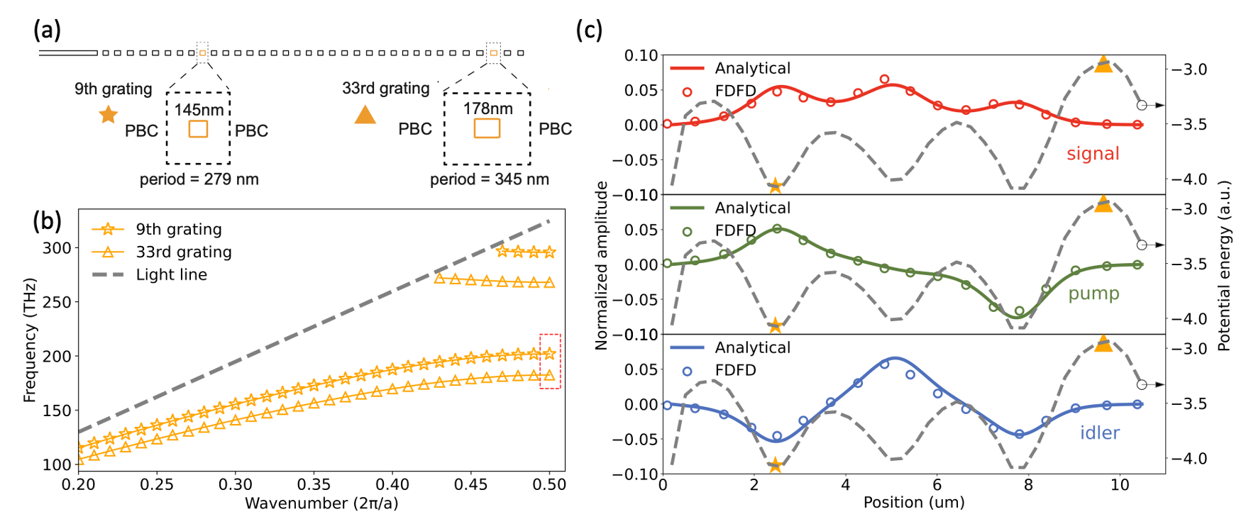
The proposed cavity device can be seen as a quasi-one-dimensional photonic crystal with small perturbations. In that sense, our inverse design strategy can be understood as optimizing the perturbation and consequent mode field profiles to achieve maximal overlap integral while keeping the resonant frequencies equally spaced. Each mode field profile can be written as a product of the band edge mode and a slowly varying envelope function ; . The envelope of a resonance mode in a perturbed photonic crystal approximately follows the Wannier-like equation40; 41,
| (2) |
where , and are the effective mass, effective potential, and the resonance frequency of the mode, respectively. The effective mass is defined by in analogy with that of electrons in solids, where is the photonic band frequency of the unperturbed photonic crystal. The effective local potential can be extracted by simulating each grating with periodic boundary conditions (PBC). Two unit-cells with relatively small (star marker) and large (triangle marker) periods are highlighted as examples. The valence band edge frequencies are calculated using finite-element simulation, shown as the dashed box in Fig. 4(b). The calculation is performed over each of the gratings, and the obtained 1D effective potential is shown as dashed grey lines in Fig. 4(c), as the square of the valence band edge frequencies. The envelope function solutions for Eq. (2) are plotted in Fig. 4(c). The envelopes show good agreement with the fields extracted from the FDFD solver in EMopt. Interestingly, the effective potential has three wells in the middle of the cavity region and a high wall near the right end. Therefore, the inverse-designed cavity can be interpreted as a three-coupled-resonator system between a highly reflective mirror on the right and an output coupler on the left. Compared with a single cavity case, the coupled-resonator configuration provides more degrees of freedom to adjust the optical mode shapes and, thus, a larger nonlinear overlap integral. In addition, our design method allows the device to have a smaller footprint for a given target resonance frequency, which is also advantageous for stronger light confinement.
VI Discussion
In summary, we propose an interpretable, computationally efficient optimization method for designing quantum and nonlinear photon generation devices on-chip. The method is demonstrated with a compact, fabrication-friendly, and highly reproducible device for photon pair generation in silicon photonics. The proposed method can be generalized for other nonlinear photon generation processes, for example, on-chip spontaneous parametric down-conversion, and third harmonic generation to cite a few. In addition, the target frequencies of the photon generation process can be chosen based on applications, which opens opportunities for inverse-design frequencies conversion across different bands, microwave-to-optic conversion, for example. The demonstrated photon-pair generation provides a feasible path for the compact integrated quantum light source. The design is also foundry compatible and can be used in scalable classical and quantum communication and computing applications based on integrated photonics platform.
References
- Fukuda et al. (2005) H. Fukuda, K. Yamada, T. Shoji, M. Takahashi, T. Tsuchizawa, T. Watanabe, J.-i. Takahashi, and S.-i. Itabashi, Optics Express 13, 4629 (2005).
- Signorini et al. (2018) S. Signorini, M. Mancinelli, M. Borghi, M. Bernard, M. Ghulinyan, G. Pucker, and L. Pavesi, Photonics Research 6, 805 (2018).
- Lin et al. (2014) Z. Lin, T. Alcorn, M. Loncar, S. G. Johnson, and A. W. Rodriguez, Physical Review A 89, 1 (2014).
- O’Brien et al. (2015) K. O’Brien, H. Suchowski, J. Rho, A. Salandrino, B. Kante, X. Yin, and X. Zhang, Nature Materials 14, 379 (2015).
- Turner et al. (2008) A. C. Turner, M. A. Foster, A. L. Gaeta, and M. Lipson, Optics Express 16, 4881 (2008).
- Azzini et al. (2012) S. Azzini, D. Grassani, M. J. Strain, M. Sorel, L. G. Helt, J. E. Sipe, M. Liscidini, M. Galli, and D. Bajoni, Optics Express 20, 23100 (2012).
- Engin et al. (2013) E. Engin, D. Bonneau, C. M. Natarajan, A. S. Clark, M. G. Tanner, R. H. Hadfield, S. N. Dorenbos, V. Zwiller, K. Ohira, N. Suzuki, H. Yoshida, N. Iizuka, M. Ezaki, J. L. O’Brien, and M. G. Thompson, Optics Express 21, 27826 (2013).
- Kumar et al. (2014) R. Kumar, J. R. Ong, M. Savanier, and S. Mookherjea, Nature Communications 5, 1 (2014).
- Grassani et al. (2015) D. Grassani, S. Azzini, M. Liscidini, M. Galli, M. J. Strain, M. Sorel, J. E. Sipe, and D. Bajoni, Optica 2, 88 (2015).
- Preble et al. (2015) S. F. Preble, M. L. Fanto, J. A. Steidle, C. C. Tison, G. A. Howland, Z. Wang, and P. M. Alsing, Physical Review Applied 4, 1 (2015).
- Ma et al. (2017) C. Ma, X. Wang, V. Anant, A. D. Beyer, M. D. Shaw, and S. Mookherjea, Optics Express 25, 32995 (2017).
- Mittal et al. (2018) S. Mittal, E. A. Goldschmidt, and M. Hafezi, Nature 561, 502 (2018).
- Bruch et al. (2019) A. W. Bruch, X. Liu, J. B. Surya, C.-L. Zou, and H. X. Tang, Optica 6, 1361 (2019).
- Guidry et al. (2020) M. A. Guidry, K. Y. Yang, D. M. Lukin, A. Markosyan, J. Yang, M. M. Fejer, and J. Vučković, Optica 7, 1139 (2020).
- Zhang et al. (2021) Y. Zhang, M. Menotti, K. Tan, V. D. Vaidya, D. H. Mahler, L. G. Helt, L. Zatti, M. Liscidini, B. Morrison, and Z. Vernon, Nature Communications 12, 8 (2021).
- Ramesh et al. (2022) A. Ramesh, I. Wang, D. Kramnik, J. M. Fargas Cabanillas, V. Stojanović, M. A. Popović, and P. Kumar, Optics InfoBase Conference Papers , 3 (2022).
- Zhao et al. (2020) J. Zhao, C. Ma, M. Rüsing, and S. Mookherjea, Physical Review Letters 124, 163603 (2020).
- Lu et al. (2021) J. Lu, A. Al Sayem, Z. Gong, J. B. Surya, C.-L. Zou, and H. X. Tang, Optica 8, 539 (2021).
- Marty et al. (2021) G. Marty, S. Combrié, F. Raineri, and A. De Rossi, Nature Photonics 15, 53 (2021).
- Kodigala et al. (2017) A. Kodigala, T. Lepetit, Q. Gu, B. Bahari, Y. Fainman, and B. Kanté, Nature 541, 196 (2017).
- Contractor et al. (2022) R. Contractor, W. Noh, W. Redjem, W. Qarony, E. Martin, S. Dhuey, A. Schwartzberg, and B. Kanté, Nature 608, 692 (2022).
- Borel et al. (2004) P. I. Borel, A. Harpøth, L. H. Frandsen, M. Kristensen, P. Shi, J. S. Jensen, and O. Sigmund, Optics Express 12, 1996 (2004).
- Burger et al. (2004) M. Burger, S. J. Osher, and E. Yablonovitch, IEICE Transactions on Electronics E87-C, 258 (2004).
- Preble et al. (2005) S. Preble, M. Lipson, and H. Lipson, Applied Physics Letters 86, 1 (2005).
- Molesky et al. (2018) S. Molesky, Z. Lin, A. Y. Piggott, W. Jin, J. Vucković, and A. W. Rodriguez, Nature Photonics 12, 659 (2018).
- Chakravarthi et al. (2020) S. Chakravarthi, P. Chao, C. Pederson, S. Molesky, A. Ivanov, K. Hestroffer, F. Hatami, A. W. Rodriguez, and K.-M. C. Fu, Optica 7, 1805 (2020).
- Pestourie et al. (2022) R. Pestourie, W. Yao, B. Kanté, and S. G. Johnson, ACS Photonics 10, 854 (2022).
- Li et al. (2022) Z. Li, R. Pestourie, Z. Lin, S. G. Johnson, and F. Capasso, ACS Photonics 9, 2178 (2022).
- Jiang et al. (2021) J. Jiang, M. Chen, and J. A. Fan, Nature Reviews Materials 6, 679 (2021).
- Lin et al. (2016) Z. Lin, X. Liang, M. Lončar, S. G. Johnson, and A. W. Rodriguez, Optica 3, 233 (2016).
- Hughes et al. (2018) T. W. Hughes, M. Minkov, I. A. Williamson, and S. Fan, ACS Photonics 5, 4781 (2018).
- Khoram et al. (2019) E. Khoram, A. Chen, D. Liu, L. Ying, Q. Wang, M. Yuan, and Z. Yu, Photonics Research 7, 823 (2019).
- Yang et al. (2023) J. Yang, M. A. Guidry, D. M. Lukin, K. Yang, and J. Vučković, (2023), arXiv:2303.17079 .
- Michaels and Yablonovitch (2018) A. Michaels and E. Yablonovitch, Optics Express 26, 31717 (2018).
- Jiang and Fan (2019) J. Jiang and J. A. Fan, Nano Letters 19, 5366 (2019).
- Hooten et al. (2021) S. Hooten, R. G. Beausoleil, and T. Van Vaerenbergh, Nanophotonics 10, 3843 (2021).
- Michaels et al. (2020) A. Michaels, M. C. Wu, and E. Yablonovitch, IEEE Journal of Selected Topics in Quantum Electronics 26, 1 (2020).
- Zhu et al. (1997) C. Zhu, R. H. Byrd, P. Lu, and J. Nocedal, ACM Transactions on Mathematical Software 23, 550 (1997).
- Ma and Mookherjea (2020) C. Ma and S. Mookherjea, OSA Continuum 3, 1138 (2020).
- Charbonneau-Lefort et al. (2002) M. Charbonneau-Lefort, E. Istrate, M. Allard, J. Poon, and E. H. Sargent, Physical Review B 65, 1253181 (2002).
- Painter et al. (2003) O. Painter, K. Srinivasan, and P. E. Barclay, Physical Review B 68, 352141 (2003).