HyDe: A Hybrid PCM/FeFET/SRAM Device-search for Optimizing Area and Energy-efficiencies in Analog IMC Platforms
Abstract
Today, there are a plethora of In-Memory Computing (IMC) devices- SRAMs, PCMs & FeFETs, that emulate convolutions on crossbar-arrays with high throughput. Each IMC device offers its own pros & cons during inference of Deep Neural Networks (DNNs) on crossbars in terms of area overhead, programming energy and non-idealities. A design-space exploration is, therefore, imperative to derive a hybrid-device architecture optimized for accurate DNN inference under the impact of non-idealities from multiple devices, while maintaining competitive area & energy-efficiencies. We propose a two-phase search framework (HyDe) that exploits the best of all worlds offered by multiple devices to determine an optimal hybrid-device architecture for a given DNN topology. Our hybrid models achieve upto higher at higher energy-efficiencies than baseline homogeneous models for a VGG16 DNN topology. We further propose a feasible implementation of the HyDe-derived hybrid-device architectures in the 2.5D design space using chiplets to reduce design effort and cost in the hardware fabrication involving multiple technology processes.
Index Terms:
In-Memory Computing, Hybrid-device Architecture, Non-idealities, Area & Energy-efficiency, 2.5D chiplet-integrationI Introduction
Deep Neural Networks (DNNs) have become ubiquitous for a wide range of applications ranging from computer vision, voice recognition to natural language processing [1]. Today, In-Memory Computing (IMC) has become popular as an alternative platform addressing the ‘memory-wall’ bottleneck of von-Neumann architectures for energy-efficient implementation of DNNs [2]. Specifically, analog crossbars based on a plethora of emerging (beyond-SRAM) IMC devices such as RRAMs, PCMs, FeFETs have been widely researched for compact, energy-efficient and accurate inference of DNNs [3].
Owing to device non-idealities and limited device precisions greatly impacting analog-based computing and the high cost of programming associated with the emerging IMC devices, traditional SRAM-based IMCs are used for accurate DNN inference on hardware [4, 5]. However, as shown in Fig. 1(a) (Area chart) for a VGG16 DNN architecture mapped onto an SRAM-based IMC hardware, the SRAM crossbars account for a significant portion of the overall chip area () [6]. Now, suppose the same DNN is mapped onto an IMC hardware based on FeFET crossbars, then the area expenditure of the IMC crossbars is of the overall chip area. However, this compactness comes at the cost of increased device-level non-idealities as well as higher device-programming costs [2]. Furthermore, emerging devices like FeFETs have poor retention capabilities (), and thus need to be frequently re-programmed to overcome accuracy degradation on hardware [7]. Thus, the device-programming energy becomes an important component of the total inference energy on hardware. As shown in Fig. 1(a) (Energy chart) for the VGG16 DNN architecture mapped onto an FeFET-based IMC hardware, programming energy accounts for of the total chip-energy. PCM devices, albeit have better retention, are more susceptible to high device-to-device variations during read operations [8, 7] resulting in reduced inference accuracies on hardware. Clearly, we see an accuracy-energy-area trade-off where, each IMC device has its own pros and cons and there is no clear winner when a full DNN model is deployed on IMC hardware using a single device (see Fig. 1(b)). Thus, device-level heterogeneity in an IMC architecture can exploit the best of all the worlds. This can help achieve high area-efficiency & inference accuracy resilient to the impact of device-specific non-idealities, while maintaining reasonably high retention at lower programming costs.
Recently there have been works based on hybrid RRAM/SRAM IMC architectures. [9, 10] improve the noise-resilience of IMC hardware during training by decomposing dot-product computations into digital boolean operations and analog Vector-Matrix-Multiplications (VMMs). This is done using SRAMs to encode the MSBs and RRAMs for the LSBs of multi-bit weights, while maintaining reasonably high energy-efficiency. [11] is also based on hybrid synapses (using FeFET and SRAM), wherein the fundamental structure of an SRAM cell is altered by embedding the FeFET device inside an SRAM cell. This is unlike other types of hybrid synapse works such as [10, 9] that require an ensemble of SRAM and an emerging device for encoding multi-precision weights. [5, 12], on the other hand, propose a heterogeneous IMC architecture for training DNNs that integrates an analog RRAM-based crossbar macro with a small digital SRAM macro to compensate for the RRAM-level noises and recover the performance accuracy, with minimal hardware overhead. A recent work called ReHy [13] proposes a hybrid-device neural training accelerator, which performs forward propagation using RRAM-based IMCs, and computes gradients during backward propagation with digital SRAM macros at floating point precision.
All the above works based on hybrid-device IMC are essentially optimizing the hardware in isolation for better noise-resilience and energy-efficiency during training or inference. However, these works are agnostic to the topology of the DNN model to be mapped onto the IMC hardware. The layer configurations of a DNN as well as the trained weights contained in these layers impact the DNN noise-resiliency, area and energy expenditures on IMC-based hardware differently. This motivates us to introduce device-level heterogeneity into our hardware architecture for DNNs, wherein each convolutional layer has affinity for one specific type of IMC device.
Our methodology of searching the design space to derive optimal hybrid-device IMC architectures (based on PCM/FeFET/SRAM devices) for a given DNN topology is termed as HyDe. We choose PCM, FeFET & SRAM-based IMC devices as they vary greatly in terms of IMC area, ON/OFF ratios, noise characteristics, retention capabilities, programming costs, thereby providing HyDe with the scope for optimization across multiple conflicting objectives (see Fig. 1(b)). While there has been a body of works based on Neural Architecture Search (NAS) [14, 15, 16, 17, 18, 19, 20] that optimize DNN topologies to meet the constraints of a given underlying hardware architecture (CPU, GPU, digital systolic-arrays, IMC and so forth) without incurring accuracy losses, this work for the first time delves deeper into the IMC device-level properties to search for an optimal combination of IMC devices to efficiently realize a fixed DNN topology on hardware. We also propose the method to implement our HyDe-derived hybrid-device models on a IMC crossbar-based monolithic chip for feasible heterogeneous integration. Furthermore, with the advent of the 2.5D/3D roadmap to solve the existing bottlenecks of heterogenenous integration in terms of cost and scalability by using chiplet-technology [21, 22, 23], our proposed vision to implement DNNs on a multi-device IMC architecture can become highly pragmatic.
In summary, the key contributions of this work are:
-
•
We propose HyDe framework for searching layer-specific hybrid-device IMC architectures (based on PCM, FeFET and SRAM devices) for noise-tolerant (accurate), area- & energy-efficient implementations of a fixed DNN model. The hybrid-device architectures have optimal retention capabilities at reasonably low programming costs (see Fig. 1(b)). Please note that the HyDe framework is not limited to searching hybrid-device IMC architectures based on PCM, FeFET and SRAM devices only but can be used for any other IMC device whose properties (such as, precision, ON/OFF ratio, noise-profile, programming energy, etc.) are input to the framework.
-
•
We also find that a layerwise hybrid-device configuration also translates to layer-specific hybrid ADC precision, leading to increased and energy-efficiency during inference.
-
•
We use a VGG16 DNN model for CIFAR10 [24] & TinyImagenet [25] tasks/datasets for our experiments. For the TinyImagenet dataset, we find that HyDe-searched hybrid model can achieve close to ‘All SRAM’ inference performance accuracy of 52.62% and as high as 6.49, with optimally high retention () at a reasonably low device-programming cost ().
-
•
We also find that the HyDe-derived hybrid-device configurations searched using CIFAR10 dataset transfer well to the more complex TinyImagenet dataset, thereby alleviating the need for chip re-fabrication for inferring a different task of the same kind.
-
•
We finally propose a pragmatic implementation of the HyDe-derived hybrid-device architectures in the 2.5D design space using an ensemble of device-specific IMC chiplets.
II Background
II-A IMC Crossbar Architectures
Analog crossbars consist of 2D arrays of IMC devices, Digital-to-Analog Converters (DACs), Analog-to-Digital Converters (ADCs) and a programming circuit. The synaptic devices at the cross-points are programmed to a particular value of conductance (between and ) during inference. For dot-product operations, the DNN activations are fed in as analog voltages to each row using DACs and weights are programmed as synaptic device conductances () at the cross-points as shown in Fig. 1(c) [26, 27, 2, 28]. For an ideal crossbar array, during inference, the voltages interact with the device conductances and produce a current (governed by Ohm’s Law). Consequently, by Kirchoff’s current law, the net output current sensed by ADCs at each column or Bit-line (BL) is the sum of currents through each device, i.e. .
Impact of non-idealities: In reality, the analog nature of the computation leads to various hardware noise or non-idealities, such as interconnect parasitic resistances, IMC device-level variations and so forth[26, 29]. Consequently, the net output current sensed at each column in a non-ideal scenario becomes , which deviates from its ideal value. This manifests as accuracy degradation for DNNs mapped onto crossbars. In this work, we deal with two specific device non-idealities during inference- read noise and temporal drift noise (illustrated in Fig. 1(c)). IMC devices exhibit device-to-device variations in their conductances that constitute the read noise , where signifies the standard-deviation of noise [29]. The noisy conductance can be written as:
| (1) |
Memristor devices, like PCMs and FeFETs, are also susceptible to temporal drift in their conductances and with the passage of time, their programmed conductance decreases and approaches higher resistance states (see Fig. 1(c)) [29]. The effect of temporal drift can be modelled using the equation:
| (2) |
Here, denotes time elapsed since programming the device to conductance at time ( is assumed to be 1s) and denotes the device-specific drift coefficient. Higher the value of , poorer the retention of the device during inference. Note, in our experiments denotes the inference time at which accuracy of a DNN is measured and denotes the time when initial inference accuracy is measured without taking the impact of temporal drift noise.
III Methodology and Implementation
III-A Parent Architecture
HyDe searches for a layerwise optimal hybrid device configuration for a given DNN and task from a parent architecture. As shown in Fig. 2(a), the parent architecture is constructed from the fixed DNN model (VGG16 in this work), wherein each 2D convolution (conv2D) operation is replaced with a Composite Device-aware Convolution (CompDC) operation. If we use different kinds of devices, then the output of a CompDC operation is a weighted-sum of the outputs of device-aware conv2D operations using each of the devices. Each constituent device-aware convolution in a CompDC layer is associated with a affinity-parameter (). Let us assume that a CompDC layer is associated with the affinity-parameters , and corresponding to three devices- SRAM, PCM and FeFET. If , and are respectively the softmax of , and and , and are the outputs of the device-aware convolutions for the individual devices, then the output of the CompDC operation () is computed as:
| (3) |
where,
| (4) |
Here, we denote [0,1] corresponding to each device constituting the CompDC operation as probability coefficient. Our objective is to train the affinity-parameters corresponding to every CompDC layer in the parent architecture (see Section III-C) and finally, sample the device with the highest affinity for every DNN layer, and, thereby obtain a hybrid-device configuration.
III-B System Implementation
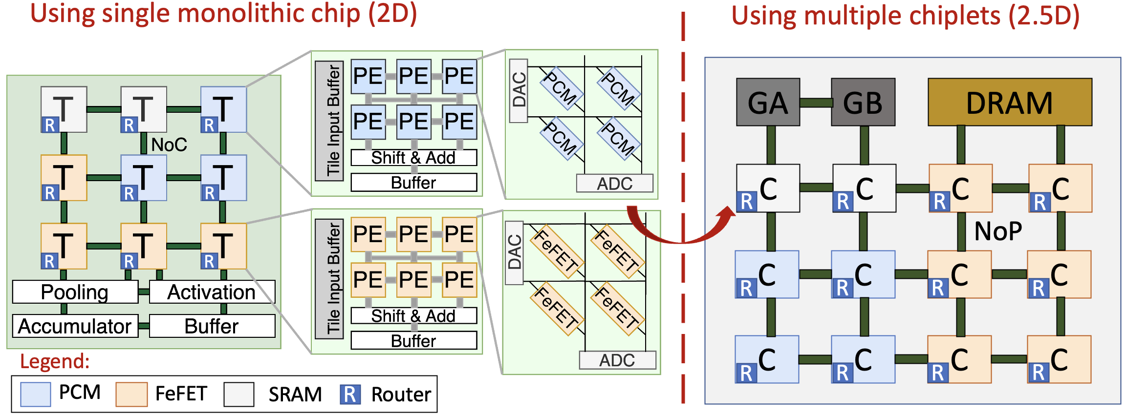
Before delving into the training methodology of HyDe, we first explain how to map a hybrid-device configuration onto a hierarchical analog crossbar-based monolithic chip [6] for inference (see illustration in Fig. 2(b)). The entire chip consists of an array of Tiles (T) that are inter-connected using a Network-on-Chip (NoC), along with buffers, accumulators, activation units and pooling units implemented digitally. Within each tile, we have an array of IMC Processing Engines (PEs) inter-connected using a H-Tree and other digital peripherals. Each PE, consisting of one analog crossbar-array of a fixed size and its peripheral circuits such as DACs and ADCs, generates dot-product outputs. Note, each tile consists of a fixed number of PEs (and hence, crossbars) and the topology of a given DNN model dictates the total number of tiles required by the chip to map the entire neural network. Within a tile, all the crossbar-arrays (existing inside the PEs) have synapses of the same device-type (i.e., SRAM, PCM or FeFET). No two layers of a DNN can be mapped onto the PEs inside a single tile [6].
Let us suppose that our hybrid-device configuration for a 4-layered DNN model (see Fig. 2) is such that the first two-layers (L1 and L2) have affinity towards SRAM crossbars, while L3 and L4 layers have affinity towards PCM and FeFET crossbars, respectively. Based on the DNN topology, let us consider that L1 and L2 need 1 tile each to be mapped, while L3 and L4 need 3 and 4 tiles, respectively. Thus, the monolithic chip would consist of 2 SRAM-based tiles (grey), 3 PCM-based tiles (blue) and 4 FeFET-based tiles (orange) as shown in Fig. 2(b). Note, the digital peripheral circuits around the array of PEs inside a tile and around the array of tiles in the chip are not disturbed by the device-level heterogeneity across tiles and hence, need not be custom designed.
For our HyDe search, the properties of the different IMC devices (SRAM, PCM & FeFET) used for hybrid-mapping on crossbars are listed in Table I. SRAM crossbars are less impacted by noise, have the highest retention and least programming energy, making them prospective candidates for accurate inference. However, SRAMs consume higher IMC area in comparison to other memristor devices. PCMs and FeFETs enable compactness during inference by reducing IMC area but are impacted by read noise and higher programming energies. Specifically, FeFETs suffer from the problem of lower retention () due to higher temporal drift coefficient for which they need to be periodically re-programmed for accurate inference [7]. PCMs, on the other hand, have better retention capabilities () [7]. However, PCM is more prone to the impact of read noise (due to larger and smaller ON/OFF ratio) than FeFET.
III-C Training Methodology of HyDe
Here, we discuss our HyDe framework which trains the device-specific affinity-parameters, thereby helping us deduce the optimal hybrid-device configuration for a given DNN model and task. We run the HyDe framework for 30 epochs. One epoch of training the parent architecture occurs in two phases (see Fig. 3) as follows:
Phase-1: Training the weight parameters. A batch of inputs with a large batch-size (1000 in this work) is randomly sampled from the Training dataset and forwarded through the parent architecture once. Thereafter, the weight parameters () for all the CompDC layers in the parent architecture are updated using backpropagation with standard cross-entropy loss (). Note, during Phase-1, we do not include any device-related parameters and the affinity-parameters () are unaffected in this phase.
Phase-2: Training the affinity-parameters. We first incorporate the impact of the device-specific properties (listed in Table I)-temporal drift, read noise and quantization on the weights () of the parent architecture in the manner shown in Fig. 3. We convert the weights into device conductances and then, incorporate device-noise in two steps. First, we include the impact of temporal conductance drift (if applicable) to the conductances using eq. 2. Unless otherwise mentioned, the value of inference time is taken as 100s to compute drift noise. Second, we add read-noise to the conductances based on the values of in Table I using eq. 1. Thus, we obtain noisy conductances which are uniformly quantized based on the precisions in Table I to . Finally, is transformed back to the weight-domain and we obtain the modified weights . Thereafter, the modified weights () are kept frozen. We train the parameters by feeding in inputs from a mini-subset of the training dataset (described in Section IV) using a modified loss objective function () via backpropagation. Note, after training the parameters, we restore the original in the parent architecture.
We follow a differentiable approach [15] to optimize for IMC crossbar area and device-programming energy by regularizing our loss objective function. Say, for the CompDC layer, the total IMC area and Programming energy with the device (SRAM, PCM or FeFET) be & , respectively. Note that & are computed using the individual device-specific areas and programming energies listed in Table I. Since, the constituent devices of a CompDC layer are associated with probability-coefficients (’s), the expected values of total IMC area () and total programming energy () for CompDC layer are:
, and .
Our modified loss objective function () is defined as:
| (5) |
Here, and are hyperparameters that control the relative importance given to & , respectively, with respect to .
III-D Sampling and Training the Optimal Hybrid-device Model
Finally, based on the trained affinity-parameters, we derive the optimal hybrid-device configuration from the parent architecture by choosing the device for a CompDC layer with the highest value of or probability-coefficient. In other words, we modify eq. (3) as:
| (6) |
The optimal hybrid-device model’s weight parameters (W) are then trained to convergence using backpropagation with layerwise device-awareness in the same manner as for Phase-2 search in HyDe. However this hardware-aware training is performed using standard cross-entropy loss based on the parameters in Table I, where we only inject device-specific read noise (without drift noise) into the weights and quantize the weights (programmed as 4-bit conductances) as well as the partial-sums arising from the ADCs. Please note that although in this work, we employ a standard IMC hardware-aware training method, we believe that including more matured hardware-aware training methods [33, 34, 35] will further improve the performance accuracies of the crossbar-mapped DNN architectures.
IV Experiments and Results
| Task/Dataset | Model |
|
|
|
|
|
||||||||||||||||
|---|---|---|---|---|---|---|---|---|---|---|---|---|---|---|---|---|---|---|---|---|---|---|
| CIFAR10 | Baseline SRAM | All SRAM | 87.62 | 15.6 | 0.2 | 19.7 | 7.03 | |||||||||||||||
| Baseline PCM | All PCM | 84.24 | 0.13 | 498 | 10.4 | |||||||||||||||||
| Baseline FeFET | All FeFET | 86.83 | 0.19 | 99.6 | 10.4 | |||||||||||||||||
| Hybrid-I | F, S, P, P, F, P, F, F, P, F, F, F | 87.11 | 0.48 | 199.2 | 18.5 | 12.8 | ||||||||||||||||
| Hybrid-II | S, P, S, P, F, F, F, F, F, F, F, P | 86.84 | 0.773 | 194.0 | 18.27 | 12.6 | ||||||||||||||||
| Hybrid-III | S, P, S, P, P, F, F, F, F, F, F, P | 87.36 | 0.77 | 152.1 | 18.31 | 12.5 | ||||||||||||||||
| TinyImagenet | Baseline SRAM | All SRAM | 52.62 | 15.6 | 0.2 | 75.9 | 2.37 | |||||||||||||||
| Baseline PCM | All PCM | 47.32 | 0.13 | 498 | 2.81 | |||||||||||||||||
| Baseline FeFET | All FeFET | 50.88 | 0.19 | 99.6 | 2.82 | |||||||||||||||||
| Hybrid-I | P, P, S, F, P, F, P, F, F, F, F, F | 50.31 | 0.483 | 178.3 | 56.0 | 5.94 | ||||||||||||||||
| Hybrid-II | F, S, F, P, P, F, F, F, F, F, F, F | 50.64 | 0.487 | 136.3 | 53.3 | 6.23 | ||||||||||||||||
| Hybrid-III | S, S, F, F, P, F, F, F, F, F, F, F | 50.62 | 0.785 | 110.1 | 52.4 | 6.49 |
Experimental Setup: We build our parent architecture using a VGG16 DNN (with 12 conv2D layers, namely L1-L12) and show experimental results on benchmark tasks or datasets- CIFAR10 and TinyImagenet. The layerwise network configuration of the VGG16 model is as follows: conv (3,64), conv (64,64), M, conv (64,128), conv (128,128), M, conv (128,256), conv (256,256), conv (256,256), conv (256,256), M, conv (256,512), conv (512,512), conv (512,512), conv (512,512), M, FC. Here, M stands for max-pooling layers (with stride of 2) and FC stands for the fully-connected classifier layer. The conv2D layers are represented as conv (n_i,n_o) where, n_i & n_o denote the number of input & output channels, respectively. The CIFAR10 dataset consists of RGB images (50,000 training and 10,000 testing) of size 3232 belonging to 10 classes. The TinyImagenet dataset is a more complex dataset with RGB images (100,000 training and 10,000 testing) of size 6464 belonging to 200 classes. Note, the mini-subset of training dataset (for Phase-2 training) is constructed by randomly sampling 10% of the images from the training examples. We carry out the HyDe search for 30 epochs using Adam Optimizer with an initial learning rate of 0.06 for training the affinity-parameters. For the CIFAR10 (TinyImagenet) dataset, the optimal hybrid-device configuration models are trained to convergence for 40 (30) epochs with initial learning rate = () using Adam Optimizer.
For each dataset, we generate three optimal hybrid-device architectures using HyDe- Hybrid-I, Hybrid-II & Hybrid-III. This is done by either adjusting the relative importances of and hyperparameters against in eq. 5 (Hybrid-I & II) or by increasing Inference time () in Phase-2 search for better retention capabilities (Hybrid-III). Hybrid-I denotes the model optimized with higher importance to overall IMC area. Hybrid-II denotes the model optimized with higher importance to overall device-programming energy. Hybrid-III is generated by increasing to 1000s from 100s. Note, our baselines for comparison are full homogeneous SRAM, PCM and FeFET-based architectures. All the baselines and the hybrid-device models are trained to convergence with hardware-aware training (see Section III-D), where we consider 4-bit ADCs for the CIFAR10 dataset and 6-bit ADCs for the TinyImagenet dataset to quantize the partial-sums. We build a wrapper on top of the Neurosim tool [6] to include the impact of layerwise device-heterogeneity and compute the hardware metrics (energy, area and ) corresponding to the baselines and the hybrid architectures. Note, Neurosim is a Python-based hardware-evaluation tool that performs a holistic energy-latency-area evaluation of analog crossbar-based DNN accelerators implemented on a tiled architecture similar to Fig. 2(b). We calibrate our tool for the device properties in Table I with a crossbar size of 128128 and 64 PEs per tile in 32 nm CMOS technology node, unless stated otherwise.
Please note that although we derive hybrid-device architectures for the VGG16 topology using HyDe, we can use the HyDe framework for any fixed DNN model (such as ResNet, DenseNet, etc.). It would only require us to re-architect the parent architecture according to the new DNN topology and then run HyDe on the same to get the optimal hybrid-device architecture.
IV-A Overall Results
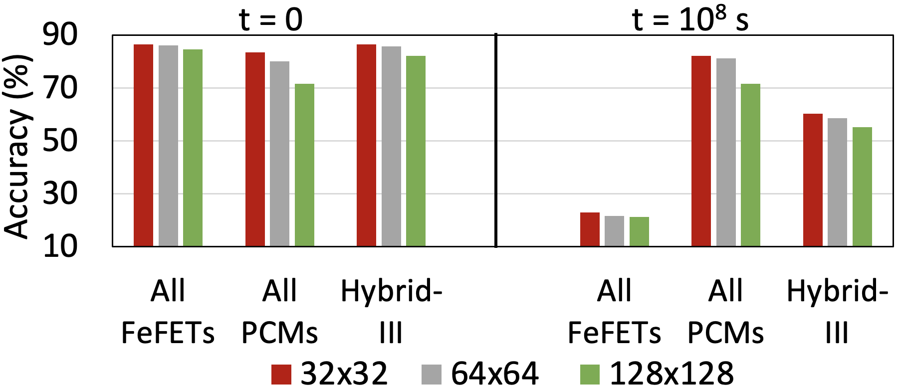
Table II shows that although the ‘All SRAM’ baseline has the best performance in terms of inference accuracy and low programming energy, it has a huge IMC area overhead and low . While the IMC area overhead gets reduced in the ‘All PCM’ baseline by , it suffers from high accuracy degradation () due to the impact of read noise and higher device-programming energy (). The ‘All FeFET’ baseline, having lower read noise, achieves better test accuracy at a lower cost of programming and with a slightly higher area () overhead than the ‘All PCM’ baseline. However, the ‘All FeFET’ baseline has the poorest retention owing to the highest temporal drift as shown in Fig. 4. In Fig. 4, the ‘All PCM’ baseline has the best retention () but has a lower initial test accuracy at due to the impact of higher read noise. Our HyDe-derived hybrid-device models achieve classification accuracy close to the ‘All SRAM’ baselines, while optimizing for area-efficiency ( more IMC area-efficient) and programming energies by reducing the average energy to . Specifically, the latter conv2D layers prefer FeFETs to reduce the impact of read noise, while maintaining optimal area-efficiency. Our hybrid models also have optimal retention capabilities (Hybrid-III being the best with reasonably low device-programming energies) as shown in Fig. 4. This is done by preferring SRAM/PCM devices in the initial layers. The discussion on increased and reduced inference energies of the hybrid models is presented in Section IV-B.
| Model | %Inference accuracy (t=0) | Average prog. energy () | Inference energy () | |||
|---|---|---|---|---|---|---|
| Hybrid-III | 50.62 | 110.1 | 125.0 | 6.49 | ||
|
50.84 | 152.1 | 128.0 | 6.04 |
IV-B Impact on ADC Precisions and Overall
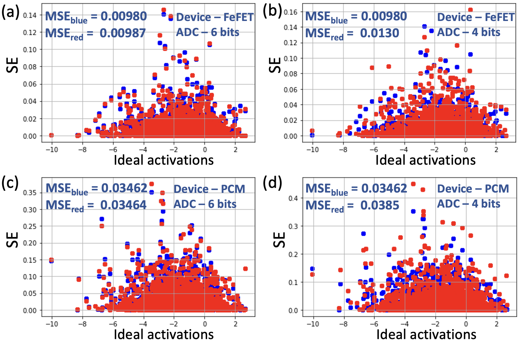
One interesting consequence of using layerwise hybrid devices is that the layerwise ADC precisions can be varied depending upon the choice of the device. Let us understand this from the analysis shown in Fig. 5. We know that FeFET is less impacted by read noise than PCM due to lower and higher ON/OFF ratio (see Table I). For Fig. 5(a-b), we take a pre-trained VGG16 model and map layer L5 using FeFET devices. We plot the squared-errors (SEs) between the noisy and ideal output activations against the ideal output activations (blue points). Thereafter, we quantize the noisy output activations using 6-bit (see Fig. 5(a)) and 4-bit (see Fig. 5(b)) ADCs, respectively, and plot their SEs against the ideal output activations (red points). In Fig. 5(c-d), we repeat the same procedure but using PCM devices. For all the plots, we report the mean-squared-errors (MSEs) for the blue and the red points as and , respectively. Note, the activations input to the L5 layer are the same for all the plots in Fig. 5 and generated from a random uniform distribution for a fair comparison. Clearly, for PCM-generated activations is higher than that of the FeFET-generated activations due to higher impact of PCM read noise. Quantizing the noisy activations using 4-bit ADCs deteriorates the MSEs further in case of PCM devices to 0.0385, while for FeFET devices it is still lower at 0.0130. This shows that PCM devices that are more susceptible to read noise should operate in conjunction with a higher ADC precision than FeFETs.
Based on the above observation, we set the layerwise ADC precision in the HyDe-derived hybrid IMC models depending upon the type of device chosen. PCM-based layers require ADC precision higher than FeFETs, while the SRAM-based layers can have the lowest ADC precision (as they are least impacted by stochastic read noise). With lower ADC precisions, we can significantly reduce the overall chip area as ADC accounts for a major share of the overall chip area as shown in Fig.1(a). This results in increased for the hybrid-device models (see Table II). In addition, the overall inference energy is also lowered in case of the hybrid models, owing to reduction in the ADC energy. Note, the homogeneous baseline models are based on uniform ADC precisions across all layers.
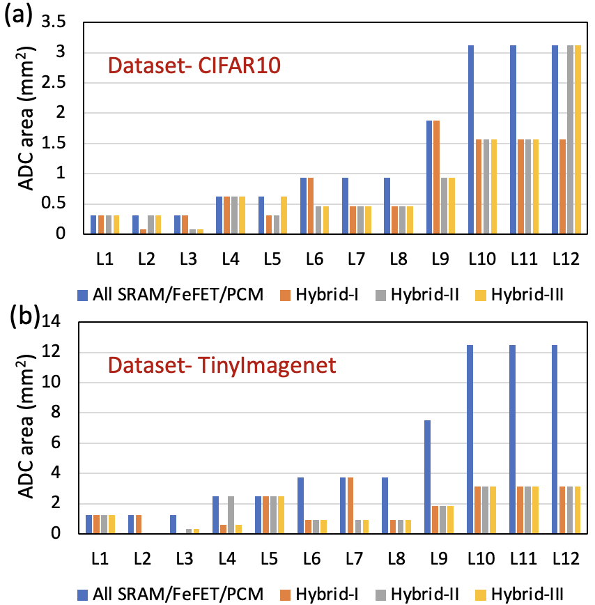
For the CIFAR10 (TinyImagenet) dataset, the minimum ADC precision to maintain the classification performance was found to be 4 bits (6 bits). Hence, all the baseline homogeneous models have 4-bit (6-bit) ADC precisions. For the hybrid models, barring the L1 layer, all SRAM-based layers have 2-bit (2-bit) ADCs, FeFET-based layers have 3-bit (4-bit) ADCs and PCM-based layers have 4-bit (6-bit) ADCs. The first layer irrespective of the nature of device requires 4-bit (6-bit) ADCs to maintain performance. In Fig. 6, as the latter conv2D layers (L5-L12) generally prefer FeFETs, the reduction in ADC precision brings huge area savings for the hybrid models against the baselines (). This boosts the of the hybrid-device models by for CIFAR10 and for TinyImagenet tasks with respect to the ‘All SRAM’ baseline. We also find a and reduction in the overall inference energy due to the layerwise heterogeneity in ADC precisions for CIFAR10 and TinyImagenet datasets, respectively.
IV-C Transferability Across Similar Tasks
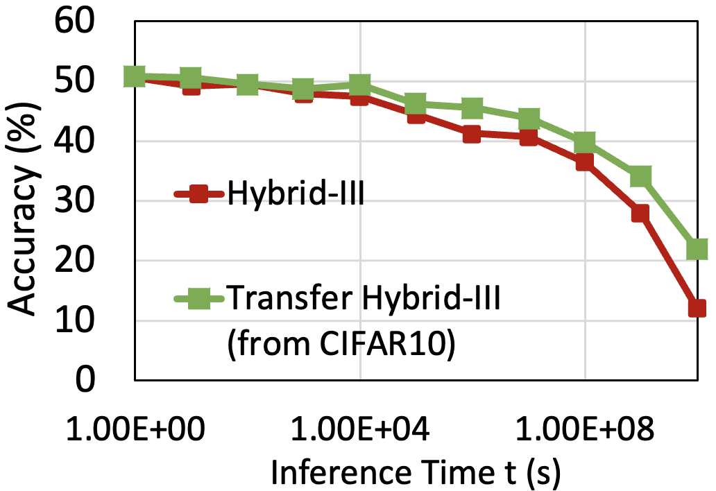
Table III and Fig. 7 show that a CIFAR10-generated hybrid-device configuration transfers well to a more complex TinyImagenet task. This eliminates chip re-fabrication costs for deploying a hybrid IMC architecture pertaining to a given DNN topology for a different task. The VGG16 DNN trained on Hybrid-III configuration transferred from CIFAR10 is iso-accurate with the Hybrid-III model for TinyImagenet and shows better retention, with marginally higher inference energy and lower . Also, since TinyImagenet is a larger dataset (100,000 training images) with larger image size (6464), the total training time per epoch for HyDe search is higher than its CIFAR10 counterpart. With transferability, we need not re-run HyDe for the TinyImagenet dataset, thereby saving on the overall training time.
IV-D Impact of Resistive Non-idealities & Crossbar Size
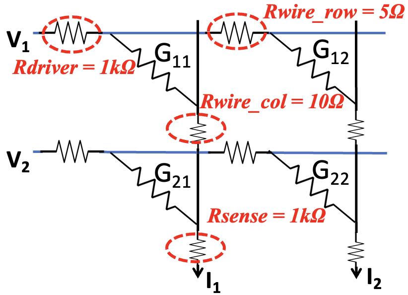
Here, we include the resisitive parasitic non-idealities (annotated in Fig. 8 with values) in crossbars during inference [27, 36]. The impact of the resistive non-idealities on the DNN weights is simulated using the RxNN framework [26]. Prior works [27, 37] have shown that larger crossbars are invariably more prone to the impact of resistive non-idealities, thereby degrading the accuracy of the mapped DNNs. Furthermore, crossbars having IMC devices with higher help reduce the impact of such non-idealities [27, 38].
| Work |
|
Technology |
|
|
|
|
||||||||||||||
| [21] | 2.5D | RRAM+CMOS |
|
N.A. | ||||||||||||||||
| [39, 40] | 2.5D |
|
|
N.A. | N.A. | |||||||||||||||
| [41] | 2.5D | RRAM+CMOS |
|
N.A. | ||||||||||||||||
| [22] | 3D | RRAM+CMOS |
|
N.A. | N.A. | |||||||||||||||
| Our work | 2.5D |
|
|
N.A. |
Fig. 9 shows the inference accuracy (CIFAR10) of the baselines and hybrid models across different crossbar sizes. At , the ‘All FeFET’ baseline with the highest suffers the least accuracy loss ( loss) , while the ‘All PCM’ baseline (lower ) has the least inference accuracy and incurs the highest degradation at higher crossbar size of 128128 ( loss). Our Hybrid-III model achieves iso-accuracy with the ‘All FeFET’ baseline for 3232 & 6464 crossbars and reduces the accuracy loss to at higher crossbar size of 128128. At , the ‘All FeFET’ baseline with poor retention, achieves close to accuracy. The ‘All PCM’ baseline has the best accuracy due to the higher retention but suffers accuracy loss at 128128 crossbars. Our Hybrid-III model maintains test accuracy with a degradation of at 128128 crossbars.
V Proposed Implementation of HyDe-derived Architectures in the 2.5D Design Space
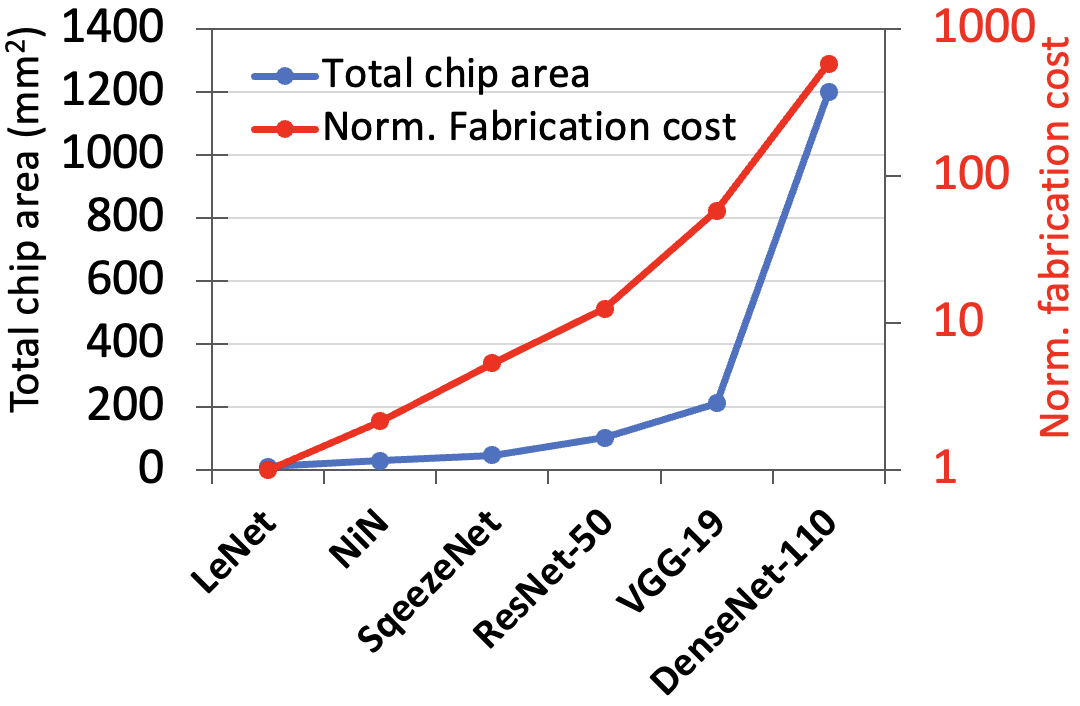
So far we have shown results upon implementing the hybird-device IMC architectures on a single monolithic chip. However, the fabrication complexity and design effort for a such a chip increases as multiple processes are involved in the fabrication of multi-device IMC architectures. In addition, larger and branched DNN topologies with higher on-chip memory requirements can incur huge on-chip area, and thus fabrication costs. From Fig. 10(a), we find that the fabrication costs (plotted in logarithmic scale) increases exponentially with the chip area, thereby making monolithic chip-design less cost-efficient, especially for larger DNNs, if all the DNN parameters are to be stored on a single chip [21]. Larger chips with hybrid IMC device integration will suffer from lower yield and higher defects across the wafer owing to multiple design processes involved, which will exacerbate the fabrication costs [42].
To circumvent the above challenges with monolithic integration, 2.5D integration using chiplet-based IMC architectures can come handy, leading to reduction in the fabrication costs [21]. While 2.5D von-Neumann inference accelerators have been proposed using chiplets containing systolic-arrays of digital dot-product engines [43, 44], there lies great promise in the domain of 2.5D analog crossbar-based IMC accelerators which have shown higher energy-efficiency [21] against their von-Neumann counterpart [43] in accelerating identical DNN workloads. To this end, in this work, we propose fabricating IMC device-specific chiplets, where each chiplet (C) consists of arrays of crossbars of a particular device-type (SRAM, PCM or FeFET) and associated peripheral circuits. As shown in Fig. 10(b), a large DNN model can be deployed on multiple smaller chiplets, wherein a single DNN layer is built upon one or more independently fabricated chiplets of a specific device-type determined by the HyDe framework. All the chiplets along with the global accumulator (GA), global buffer (GB) and DRAM are integrated into a Package and interconnected using an Network-on-Package (NoP) that uses package-level signalling to connect different chiplets [45, 46]. Using an ensemble of small-sized device-specific chiplets helps improve the design effort and yield, reduces defect ratio and the fabrication cost in supporting multiple process technologies, thereby making our proposal for heterogeneous device-integration in the hardware implementation of deep learning workloads more pragmatic. Additionally, the 2.5D heterogeneous chiplet architecture is scalable to larger and complex DNN topologies as their constituent layers can be built by integrating chiplets of a particular design process [21].
Table IV presents a qualitative comparison of our work in relation to previously proposed IMC implementations of deep learning workloads in the 2.5D/3D roadmap, highlighting our key contributions.
VI Conclusion
We propose HyDe framework that searches the layerwise affinity of a DNN for different IMC devices (PCM/FeFET/SRAM) to maintain high inference accuracy and maximize hardware area and energy-efficiencies. We find our HyDe-derived hybrid models to achieve upto higher at higher energy-efficiencies than baseline homogeneous architectures. With the emergence of the 2.5D chiplet technology to facilitate heterogeneous integration on hardware, we believe our work highlighting the benefits of hybrid IMC design using multiple devices is encouraging and timely.
Acknowledgement
This work was supported in part by CoCoSys, a JUMP2.0 center sponsored by DARPA and SRC, Google Research Scholar Award, the NSF CAREER Award, TII (Abu Dhabi), the DARPA AI Exploration (AIE) program, and the DoE MMICC center SEA-CROGS (Award #DE-SC0023198).
References
- [1] Alzubaidi et al., “Review of deep learning: Concepts, cnn architectures, challenges, applications, future directions,” Journal of big Data, 2021.
- [2] A. Sebastian et al., “Memory devices and applications for in-memory computing,” Nature nanotechnology, 2020.
- [3] I. Chakraborty et al., “Pathways to efficient neuromorphic computing with non-volatile memory technologies,” Applied Physics Reviews, 2020.
- [4] S. Spetalnick et al., “A practical design-space analysis of compute-in-memory with sram,” IEEE TCAS-I, 2022.
- [5] G. Krishnan et al., “Hybrid rram/sram in-memory computing for robust dnn acceleration,” IEEE TCAD, 2022.
- [6] Chen et al., “Neurosim: A circuit-level macro model for benchmarking neuro-inspired architectures in online learning,” IEEE TCAD, 2018.
- [7] Byun et al., “Recent advances in synaptic nonvolatile memory devices and compensating architectural and algorithmic methods toward fully integrated neuromorphic chips,” Advanced Materials Technologies, 2022.
- [8] S. Nandakumar et al., “A phase-change memory model for neuromorphic computing,” Journal of Applied Physics, 2018.
- [9] M. R. H. Rashed et al., “Hybrid analog-digital in-memory computing,” in IEEE/ACM ICCAD, 2021.
- [10] Y. Luo et al., “Accelerating deep neural network in-situ training with non-volatile and volatile memory based hybrid precision synapses,” IEEE TOC, 2020.
- [11] W.-X. You et al., “A new 8t hybrid nonvolatile sram with ferroelectric fet,” IEEE Journal of the Electron Devices Society, 2020.
- [12] P. Behnam et al., “An algorithm-hardware co-design framework to overcome imperfections of mixed-signal dnn accelerators,” arXiv:2208.13896, 2022.
- [13] H. Jin et al., “Rehy: A reram-based digital/analog hybrid pim architecture for accelerating cnn training,” IEEE TPDS, 2021.
- [14] H. Cai et al., “Once-for-all: Train one network and specialize it for efficient deployment,” arXiv:1908.09791, 2019.
- [15] Cai et al., “Proxylessnas: Direct neural architecture search on target task and hardware,” arXiv:1812.00332, 2018.
- [16] W. Jiang et al., “Hardware/software co-exploration of neural architectures,” IEEE TCAD, 2020.
- [17] K. Choi et al., “Dance: Differentiable accelerator/network co-exploration,” in ACM/IEEE DAC. IEEE, 2021.
- [18] B. Lyu et al., “Designing efficient bit-level sparsity-tolerant memristive networks,” IEEE TNNLS, 2023.
- [19] A. Bhattacharjee et al., “Xplorenas: Explore adversarially robust & hardware-efficient neural architectures for non-ideal xbars,” ACM TECS, 2023.
- [20] A. Moitra et al., “Xpert: Peripheral circuit & neural architecture co-search for area and energy-efficient xbar-based computing,” arXiv:2303.17646, 2023.
- [21] G. Krishnan et al., “Siam: Chiplet-based scalable in-memory acceleration with mesh for deep neural networks,” ACM TECS, 2021.
- [22] G. Murali et al., “Heterogeneous mixed-signal monolithic 3-d in-memory computing using resistive ram,” IEEE TVLSI, 2020.
- [23] G. H. Loh et al., “Understanding chiplets today to anticipate future integration opportunities and limits,” in IEEE DATE, 2021.
- [24] A. Krizhevsky, “Learning multiple layers of features from tiny images,” Tech. Rep., 2009.
- [25] Y. Le and X. Yang, “Tiny imagenet visual recognition challenge,” 2015.
- [26] S. Jain et al., “Rxnn: A framework for evaluating deep neural networks on resistive crossbars,” IEEE TCAD, 2020.
- [27] A. Bhattacharjee et al., “Neat: Non-linearity aware training for accurate, energy-efficient and robust implementation of neural networks on 1t-1r crossbars,” IEEE TCAD, 2021.
- [28] J. Büchel et al., “Gradient descent-based programming of analog in-memory computing cores,” in IEDM. IEEE, 2022.
- [29] Sun et al., “Impact of non-ideal characteristics of resistive synaptic devices on implementing convolutional neural networks,” IEEE JETCAS, 2019.
- [30] W. Haensch et al., “A co-design view of compute in-memory with non-volatile elements for neural networks,” arXiv:2206.08735, 2022.
- [31] P. Wang and S. Yu, “Ferroelectric devices and circuits for neuro-inspired computing,” MRS Communications, 2020.
- [32] A. Jaiswal et al., “8t sram cell as a multibit dot-product engine for beyond von neumann computing,” IEEE TVLSI, 2019.
- [33] M. J. Rasch et al., “Hardware-aware training for large-scale and diverse deep learning inference workloads using in-memory computing-based accelerators,” Nature Communications, 2023.
- [34] G. Krishnan et al., “Exploring model stability of deep neural networks for reliable rram-based in-memory acceleration,” IEEE Transactions on Computers, 2022.
- [35] Y. Wu et al., “Bulk-switching memristor-based compute-in-memory module for deep neural network training,” arXiv:2305.14547, 2023.
- [36] A. Bhattacharjee et al., “Efficiency-driven hardware optimization for adversarially robust neural networks,” in DATE. IEEE, 2021.
- [37] A. Bhattacharjee and P. Panda, “Switchx: Gmin-gmax switching for energy-efficient and robust implementation of binarized neural networks on reram xbars,” ACM TODAES, 2021.
- [38] A. Moitra et al., “Spikesim: An end-to-end compute-in-memory hardware evaluation tool for benchmarking spiking neural networks,” IEEE TCAD, 2023.
- [39] G. Krishnan et al., “System-level benchmarking of chiplet-based imc architectures for deep neural network acceleration,” in IEEE ASICON, 2021.
- [40] H. Sharma et al., “Achieving datacenter-scale performance through chiplet-based manycore architectures,” in DATE. IEEE, 2023.
- [41] Z. Wang et al., “Ai computing in light of 2.5 d interconnect roadmap: Big-little chiplets for in-memory acceleration,” in IEEE IEDM, 2022.
- [42] D. Stow et al., “Cost analysis and cost-driven ip reuse methodology for soc design based on 2.5 d/3d integration,” in IEEE/ACM ICCAD, 2016.
- [43] Y. S. Shao et al., “Simba: Scaling deep-learning inference with multi-chip-module-based architecture,” in IEEE/ACM International Symposium on Microarchitecture, 2019.
- [44] C. Liu et al., “A 256gb/s/mm-shoreline aib-compatible 16nm finfet cmos chiplet for 2.5 d integration with stratix 10 fpga on emib and tiling on silicon interposer,” in IEEE CICC, 2021.
- [45] W. J. Turner et al., “Ground-referenced signaling for intra-chip and short-reach chip-to-chip interconnects,” in IEEE CICC, 2018.
- [46] M.-S. Lin et al., “A 7-nm 4-ghz arm1-core-based cowos1 chiplet design for high-performance computing,” IEEE JSSC, 2020.