Electronic and Spin-Orbit Properties of hBN Encapsulated Bilayer Graphene
Abstract
Van der Waals (vdW) heterostructures consisting of Bernal bilayer graphene (BLG) and hexagonal boron nitride (hBN) are investigated. By performing first-principles calculations we capture the essential BLG band structure features for several stacking and encapsulation scenarios. A low-energy model Hamiltonian, comprising orbital and spin-orbit coupling (SOC) terms, is employed to reproduce the hBN-modified BLG dispersion, spin splittings, and spin expectation values. Most important, the hBN layers open an orbital gap in the BLG spectrum, which can range from zero to tens of meV, depending on the precise stacking arrangement of the individual atoms. Therefore, large local band gap variations may arise in experimentally relevant moiré structures. Moreover, the SOC parameters are small (few to tens of eV), just as in bare BLG, but are markedly proximity modified by the hBN layers. Especially when BLG is encapsulated by monolayers of hBN, such that inversion symmetry is restored, the orbital gap and spin splittings of the bands vanish. In addition, we show that a transverse electric field mainly modifies the potential difference between the graphene layers, which perfectly correlates with the orbital gap for fields up to about 1 V/nm. Moreover, the layer-resolved Rashba couplings are tunable by eV per V/nm. Finally, by investigating twisted BLG/hBN structures, with twist angles between 6∘ – 20∘, we find that the global band gap increases linearly with the twist angle. The extrapolated band gap is about 23 meV and results roughly from the average of the stacking-dependent local band gaps. Our investigations give new insights into proximity spin physics of hBN/BLG heterostructures, which should be useful for interpreting experiments on extended as well as confined (quantum dot) systems.
I Introduction
Two-dimensional (2D) materials provide a fascinating playground for investigating fundamental physics phenomena and serve as promising platforms for technological applications Cai et al. (2018), such as tunnel field-effect transistors based on monolayer transition-metal dichalcogenides (TMDCs) Kumar et al. (2020) or magnetic random access memories based on 2D magnets Zhang et al. (2019a); Gong and Zhang (2019); Li et al. (2019); Song et al. (2018). When different 2D materials are combined in van der Waals (vdW) heterostructures, new device functionalities can be engineered by the proximity effect Sierra et al. (2021).
Bernal bilayer graphene (BLG) is a prototypical electronic material which offers high electron mobility, like monolayer graphene, but also band gap engineering by an external electric displacement field McCann (2006); Min et al. (2007); McCann and Koshino (2013); Slizovskiy et al. (2021). In experiments, the band gap can be tuned up to hundreds of meV Ohta et al. (2006); Zhou et al. (2007); Oostinga et al. (2007); Mak et al. (2009); Icking et al. (2022), while the bands additionally host magnetic and superconducting phases Zhou et al. (2022); de la Barrera et al. (2022). The tunable flat bands make BLG also an interesting platform for studying electron-electron interactions Weitz et al. (2010); Geisenhof et al. (2021); Kou et al. (2014); Ki et al. (2014); Zheng et al. (2020); Seiler et al. (2022). Furthermore, BLG has low spin-orbit coupling (SOC) Kane and Mele (2005); Konschuh et al. (2012); Kurzmann et al. (2021); Banszerus et al. (2021) and weak hyperfine interaction Wojtaszek et al. (2014); Fischer and Loss (2009), which, in combination with the possibility of electrostatic confinement of charge carriers in quantum point contacts and quantum dots Overweg et al. (2018); Kurzmann et al. (2021); Eich et al. (2018); Banszerus et al. (2020); Garreis et al. (2021); Lee et al. (2020), makes it an attractive candidate for hosting spin and valley qubits Banszerus et al. (2023).
Furthermore, BLG is highly sensitive to its environment. For example, BLG on a strong spin-orbit material, such as TMDCs or topological insulators (TIs), exhibits enhanced spin interactions in the meV range Zutic et al. (2019); Zollner et al. (2018, 2019, 2020); Zollner and Fabian (2019); Omar et al. (2019); Bisswanger et al. (2022); Gmitra and Fabian (2017). In particular, for BLG on WSe2 it has been theoretically predicted Gmitra and Fabian (2017) and experimentally confirmed Island et al. (2019), that the SOC of charge carriers can be controlled by the displacement field leading to spin-orbit valve functionality. It has also been shown that WSe2 stabilizes the superconducting phase in BLG due to proximity-induced Ising SOC Zhang et al. (2023). In addition to the SOC, it is also possible to induce superconductivity Li et al. (2020a); Moriya et al. (2020) or magnetism Zollner et al. (2016, 2018, 2019) in BLG with high tunability Zollner and Fabian (2021), making it an intriguing material for various applications.
Encapsulating BLG in hexagonal boron nitride (hBN) has become a standard technique for improving its quality and stability Dean et al. (2010); Wang et al. (2013), due to the insulating nature of hBN with a band gap of 5.9 eV Watanabe et al. (2004), its high thermal conductivity Lindsay and Broido (2011); Yuan et al. (2019), and its ultra-flat surface. This technique has made it possible to build ultra-high carrier mobility devices based on graphene Dean et al. (2010); Wang et al. (2013); Banszerus et al. (2015), as well as high-quality optoelectric TMDC-devices Ajayi et al. (2017); Raja et al. (2019); Ersfeld et al. (2020), while also protecting sensitive materials from degradation under ambient conditions Gao et al. (2016); Gurram et al. (2018). Improving the quality of hBN is a focus of ongoing research efforts Meng et al. (2018); Maestre et al. (2021); Taniguchi and Watanabe (2007); Zastrow (2019); Onodera et al. (2019, 2020); Kubota et al. (2007, 2008); Hoffman et al. (2014); Edgar et al. (2014); Liu et al. (2018); Li et al. (2020b, 2021); Zhang et al. (2019b); Cao et al. (2022); Naclerio and Kidambi (2023); Ouaj et al. (2023). In addition to its encapsulation properties, recent research has shown that hBN can also have a profound effect on the bandstructure of BLG, breaking the inversion symmetry and allowing for manipulation of the induced Berry curvature Kareekunnan et al. (2020); Moulsdale et al. (2022).
In this paper we investigate theoretically, using DFT methods, the orbital and spin-orbit proximity effects in BLG/hBN and fully encapsulated hBN/BLG/hBN heterostructures. The calculated electronic structures are fitted—at low energies—with effective Hamiltonians and various quantitative parameters of the proximitized bands are extracted. We analyze the variation of the proximity band structure with stacking/encapsulation configurations, finding orbital gaps up to tens of meV. The spin-orbit splittings of bands are small, tens of eV, consistent with expectations, and with previous calculations of hBN-encapsulated monolayer graphene Zollner et al. (2019). We pay particular attention to the electric field tunability. While the electric displacement field opens a large gap, on the order of 50–100 meV for fields of 1V/nm, the field also polarizes the layers which then leads to layer-selective proximity effect. For example, the Rashba SOC is strongly influenced by the electric field, changing the sign as the field changes the polarity. We also find a rather strong enhancement of the interlayer spin-orbit coupling parameter, from 10 to more than 20 eV, due to encapsulation. Finally, we also study orbital gaps in twisted BLG/hBN heterostructures, to see spatial variation of the gaps, resolving the individual atomic orbital contributions in the spatial profile.
Although the SOC effects due to hBN are rather modest, experimentally it is now possible to resolve eV scales, most prominently in confined quantum dot structures. The experiments find SOC gaps of about 40-80 eV in hBN encapsulated BLG Banszerus et al. (2020), while the theoretical spin-orbit splittings of the infinite crystals are up to 25 eV Konschuh et al. (2012). While this discrepancy is not fully resolved, our calculations should be useful to interpret also such experiments on confined structures.
The paper is organized as follows: In section II we address the structural setup and summarize the calculation details for obtaining the electronic structures. In section III, we introduce the model Hamiltonians that capture the low-energy physics of proximitized BLG (including orbital and SOC terms), which are used to fit the DFT-calculated dispersions. In section IV, we then show and discuss the DFT-calculated electronic structures of (hBN)/BLG/hBN stacks, along with the model Hamiltonian fits, as well as the gate tunability. In section V, we study twisted BLG/hBN structures and discuss local band gap variations in moiré geometries. Finally, in section VI we conclude the manuscript.
II Computational Details and Geometry
In order to calculate the electronic band structure of (hBN)/BLG/hBN heterostructures, we use a common unit cell for graphene and hBN. Therefore, we fix the lattice constant of graphene Castro Neto et al. (2009) to Å, and change the hBN lattice constant, from its experimental value Catellani et al. (1987) of Å, to the graphene one. The lattice constants of graphene and hBN differ by less than 2%, justifying our theoretical considerations of commensurate geometries. Experimentally, the small lattice mismatch does lead to moiré patterns Jung et al. (2014); Moon and Koshino (2014); Argentero et al. (2017). Here we consider several, but not all, structural arrangements for commensurate unit cells, so as to get a quantitative feeling for spin-orbit phenomena in a generic experimental setting.
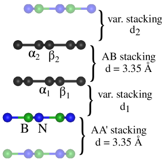
In the following, we consider BLG in Bernal (AB) stacking with a fixed interlayer distance of 3.35 Å Konschuh et al. (2012). The minimal heterostructure we study is BLG on top of monolayer hBN in different stacking scenarios, see Fig. 1. In addition, we consider BLG encapsulated by hBN layers. When bilayer hBN is considered for encapsulation, we employ an AA’ stacking also with a fixed interlayer distance of 3.35 Å Constantinescu et al. (2013). The variable stackings are between the graphene layers and the surrounding hBN layers, see Fig. 1. We use the equilibrium distances of the individual graphene/hBN stackings as found in Ref. Zollner et al. (2019). This fixes all interlayer distances in our (hBN)/BLG/hBN heterostructure geometries for all stacking sequences we consider.
Before we proceed, we define a terminology to make sense of the structural arrangements used in the following. We denote the three relevant sites in hBN as the B-site (Boron), the N-site (Nitrogen), and the H-site (hollow position in the center of the hexagon). Similarly, each graphene layer, , consists of sublattices (C) and (C) and a hollow site hj. The energetically most favorable stacking sequence, listed from bottom to top, of BLG on monolayer hBN is then abbreviated as (Bh2,H), see Fig. 1. This stacking sequence has d Å Zollner et al. (2019). In Table 1, we summarize the total energies and interlayer distances of all our investigated geometries. In addition, we consider all hBN-encapsulated structures also with bilayer-hBN below BLG (not explicitly listed in Table 1).
| Configuration | E-E0 [meV] | d1 [Å] | d2 [Å] |
|---|---|---|---|
| (Bh2,H) | 0 | 3.35 | - |
| (Nh2,H) | 13.911 | 3.50 | - |
| (Nh2,B) | 16.709 | 3.55 | - |
| (Bh2N,HH) | 0 | 3.35 | 3.35 |
| (Nh2B,HH) | 27.745 | 3.50 | 3.50 |
| (Bh2B,HH) | 13.791 | 3.35 | 3.50 |
| (Bh2H,HB) | 16.602 | 3.35 | 3.55 |
| (Nh2H,HB) | 30.556 | 3.50 | 3.55 |
| (Nh2H,BB) | 33.361 | 3.55 | 3.55 |
Initial atomic structures are set up with the atomic simulation environment (ASE) Bahn and Jacobsen (2002) and visualized with VESTA software Momma and Izumi (2011). First-principles calculations are performed with full potential linearized augmented plane wave (FLAPW) code based on DFT Hohenberg and Kohn (1964) and implemented in WIEN2k Blaha et al. (2001). Exchange-correlation effects are treated with the generalized-gradient approximation (GGA) Perdew et al. (1996), including dispersion correction Grimme et al. (2010) and using a -point grid of in the hexagonal Brillouin-Zone if not specified otherwise. The values of the Muffin-tin radii we use are for C atom, for B atom, and for N atom. We use the plane wave cutoff parameter . In order to avoid interactions between periodic images of our slab geometry, we add a vacuum of at least Å in -direction.
For some of our structures, we also study the effect of a transverse electric field. Importantly, in WIEN2k the electric field is modeled by a zigzag potential Stahn et al. (2001), that is realized by a Fourier series, and which has its discontinuities at and , where is the lattice constant in -direction. Therefore, in all our calculations we center our geometries around , similar as in Ref. Gmitra et al. (2009). A positive (negative) electric field corresponds to a decreasing (increasing) potential across our geometries.
III Model Hamiltonian
Here we present the Hamiltonian used to model the low-energy bands of the encapsulated BLG structures. The basis states are , , , , , , , and . In this basis the Hamiltonian is (see Ref. Konschuh et al. (2012))
| (1) | ||||
| (2) | ||||
| (3) |
Here, , , describe intra- and interlayer hoppings in BLG. The parameter is the nearest neighbor intralayer hopping, similar to monolayer graphene, while is the direct interlayer hopping. The parameters and describe indirect hoppings between the layers. The vertical hopping connects only 2 atoms and therefore it appears without structural function in the Hamiltonian. In contrast, the other hoppings couple an atom to 3 corresponding nearest neighbor partner atoms, hence they appear with structural function, where we use the linearized version, , valid in the vicinity of the K points Kochan et al. (2017). The graphene lattice constant is and the Cartesian wave vector components and are measured with respect to for the valley indices . In addition, the lower (upper) graphene layer is placed in the potential (). The parameter describes the asymmetry in the energy shift of the bonding and antibonding states, which arises due to the interlayer coupling . The Pauli spin matrices are , with , and .
The parameters describe the intrinsic SOC of the corresponding layer and sublattice atom (), which are modified by the hBN layer(s). The intrinsic SOC parameters are also present in pristine BLG and on the order of 12 eV Konschuh et al. (2012). The parameters and represent the Rashba SOC of the individual graphene layers, which can be opposite in sign Zollner and Fabian (2021). From the symmetry point of view, also other SOC parameters are allowed, but we restrict ourselves to add only , being the interlayer SOC term connecting same sublattices, and which is the most relevant one in pristine BLG Konschuh et al. (2012); Guinea (2010). Since we are dealing with hBN/BLG structures, the sublattice atoms are affected differently and we introduce and .
To capture doping effects from the calculations, we introduce another parameter , which leads to an energy shift on the model band structure and we call it the Dirac point energy. However, since the Fermi level is within the band gap for all our considered heterostructures, no charge transfer occurs and we set . To extract the fit parameters form the DFT, we employ a least-squares routine, taking into account band energies, splittings, and spin expectation values. First, we extract the orbital parameters, , , and . Once they are fixed, we extract the spin-orbit parameters.
IV Band Structures, Fit Results, and Gate Tunability
IV.1 Pristine BLG with electric field
| Field [V/nm] | 0 | 0.1 | 0.25 | 0.5 | 0.75 | 1.0 | 1.25 | 1.5 | 1.75 | 2.0 |
|---|---|---|---|---|---|---|---|---|---|---|
| [eV] | 2.567 | 2.567 | 2.565 | 2.563 | 2.565 | 2.565 | 2.566 | 2.567 | 2.578 | 2.569 |
| [eV] | 0.339 | 0.339 | 0.339 | 0.339 | 0.339 | 0.339 | 0.339 | 0.339 | 0.340 | 0.340 |
| [eV] | 0.274 | 0.277 | 0.277 | 0.277 | 0.276 | 0.276 | 0.276 | 0.278 | 0.280 | 0.283 |
| [eV] | -0.153 | -0.153 | -0.154 | -0.154 | -0.154 | -0.154 | -0.154 | -0.153 | -0.153 | -0.153 |
| gap [meV] | 0 | 1.290 | 5.146 | 25.613 | 50.482 | 73.813 | 95.481 | 115.323 | 133.274 | 149.361 |
| [meV] | 0 | 0.959 | 2.953 | 13.640 | 27.009 | 40.334 | 53.595 | 66.768 | 79.830 | 92.768 |
| [meV] | 9.783 | 9.783 | 9.783 | 9.783 | 9.782 | 9.780 | 9.776 | 9.772 | 9.765 | 9.760 |
| [eV] | -6.7 | -6.9 | -7.4 | -8.4 | -9.2 | -10.6 | -11.7 | -12.9 | -13.8 | -14.8 |
| [eV] | 6.7 | 6.4 | 6.1 | 5.1 | 3.7 | 2.9 | 1.8 | 0.9 | -0.3 | -1.5 |
| [eV] | 10.2 | 10.2 | 10.2 | 10.2 | 10.2 | 10.2 | 10.2 | 10.2 | 10.2 | 10.2 |
| [eV] | 12.2 | 12.2 | 12.2 | 12.2 | 12.2 | 12.2 | 12.2 | 12.2 | 12.2 | 12.2 |
| [eV] | 12.2 | 12.2 | 12.2 | 12.2 | 12.2 | 12.2 | 12.2 | 12.2 | 12.2 | 12.2 |
| [eV] | 10.2 | 10.2 | 10.2 | 10.2 | 10.2 | 10.2 | 10.2 | 10.2 | 10.2 | 10.2 |
| [eV] | 12.4 | 12.4 | 13.1 | 13.0 | 13.5 | 13.7 | 14.0 | 14.1 | 14.5 | 15.0 |
| [eV] | 12.4 | 12.4 | 12.9 | 12.4 | 12.1 | 11.9 | 11.6 | 11.5 | 11.2 | 10.9 |
The dispersion of pristine BLG features 8 parabolic bands in the vicinity of the point Konschuh et al. (2012). In addition, the BLG bands are formed by different layers and sublattices. Due to inversion symmetry of the AB-stacked BLG, bands are spin degenerate without external electric field. When a transverse electric field is applied, the two graphene layers are placed in different potentials, lifting the inversion symmetry along with spin degeneracies, and a band gap opens. Recent transport measurements have shown ultraclean band gaps in BLG heterostructures when hBN is employed as encapsulation material Icking et al. (2022). They also demonstrated that the gap can be tuned linearly with the applied electric field, in agreement with theory predictions Konschuh et al. (2012). Before we discuss the BLG/hBN heterostructures, we briefly reconsider pristine BLG in a transverse electric field to get a qualitative feeling for orbital and spin-orbit parameters, as well as the tunability of the band gap, closely following Ref. Konschuh et al. (2012).
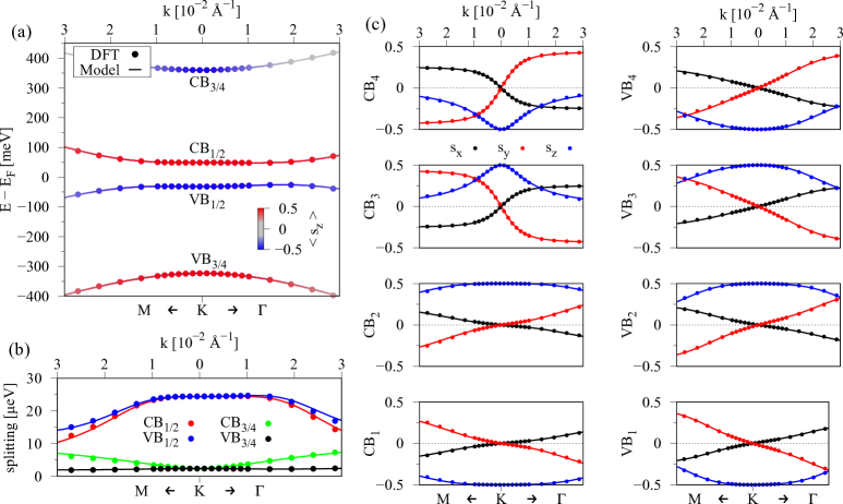
In Fig. 2, we show the calculated band properties of pristine BLG in the vicinity of the point and with an external transverse electric field of 1 V/nm. The first-principles data are perfectly reproduced by the parameters in Table 2, demonstrating the accuracy of the employed model. In contrast to Ref. Konschuh et al. (2012) we have even neglected some SOC parameters in the model, that are apparently irrelevant for reproducing the DFT results. Note that the fitting procedure is not a straightforward task, since two different energy scales are present. We have hundreds of meV from the orbital parameters and few to tens of eV from the SOC ones Konschuh et al. (2012). Focusing on band energies only, the orbital parameters were determined first employing the least-squares fitting routine. Then, we fixed the intrinsic SOC parameters for and ( and ) to about eV (eV), according to Ref. Konschuh et al. (2012). In other words, the dimer atoms have an intrinsic SOC value that is reduced by eV, compared to the non-dimer atom. Finally, we fitted for the remaining SOC parameters.
Coming back to the band structure, see Fig. 2(a), we find a band gap of about 80 meV, with corresponds to about . For the applied positive electric field, the lower graphene layer will be in a higher potential than the upper layer, fixing the sign of parameter . More specifically, the low-energy bands are formed by the non-dimer atoms in the vicinity of the point, and for the positive elecric field the bands CB1/2 (VB1/2) are formed by atom () Konschuh et al. (2012); McCann and Koshino (2013). The high-energy bands are formed by a combination of dimer atoms, which are split-off to about meV away from the Fermi level by the direct interlayer coupling . At the point, the low-energy bands show a spin-splitting of about eV corresponding to pristine graphene Konschuh et al. (2010); Gmitra et al. (2009); Konschuh et al. (2012), while the high-energy band splittings are much smaller, see Fig. 2(b).
At zero external field, the electrons in one layer feel an effective field due to the presence of the other layer, leading to Rashba SOCs of opposite signs in the two layers. Therefore, without external field, we cannot determine the value of the intrinsic Rashba parameters, since their effect on the bands cancel out. However, since an external electric field is applied the Rashba effect is activated, creating vortex-like spin textures near the point. Once an external electric field is applied, it adds to the opposing internal ones, the Rashba couplings are modified, and we can fix their values by fitting to the DFT calculation. For the electric field of 1 V/nm, we find the Rashba SOC parameters to be and eV. The Rashba SOC parameters that we can extrapolate to zero electric field, by averaging the fitted parameters at 1 V/nm, are eV for the lower/upper graphene layer. This value is reasonable following the argumentation in Ref. Konschuh et al. (2012), but does not fully agree with the value found there. However, it is of the same order of magnitude as in graphene/hBN heterostructures Zollner et al. (2019), giving us confidence in the extracted value.
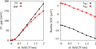
For completeness, we also summarize the fit parameters of pristine BLG without external electric field in Table 2. As we can see, the external field mainly influences the potential parameter and the Rashba couplings. In Fig. 3, we show the evolution of the potential , the band gap, and the two Rashba parameters and as function of the applied electric field. We limit ourselves to show only these parameters since the others are barely affected by the field. Both Rashba couplings follow a linear trend as expected Konschuh et al. (2012); Gmitra et al. (2009), with a tunability of about eV per V/nm. The potential parameter shows a nonlinear onset for small electric fields and a linear tunability for higher electric fields. For small electric fields the band gap also closely follows and starts to drastically deviate for fields above 1 V/nm.
The above investigation will be helpful for analyzing hBN/BLG heterostructures, since the hBN layer(s) modify the overall electrostatics and the spin-orbit parameters via proximity effect Zollner et al. (2019).
IV.2 BLG on hBN
| system | (Bh2,H) | (Nh2, H) | (Nh2,B) | |||
|---|---|---|---|---|---|---|
| el. field [V/nm] | 0 | 1.0 | 0 | 1.0 | 0 | 1.0 |
| [eV] | 2.556 | 2.544 | 2.548 | 2.525 | 2.520 | 2.543 |
| [eV] | 0.337 | 0.339 | 0.339 | 0.337 | 0.337 | 0.335 |
| [eV] | 0.271 | 0.272 | 0.271 | 0.276 | 0.277 | 0.279 |
| [eV] | -0.153 | -0.155 | -0.150 | -0.157 | -0.149 | -0.158 |
| [meV] | -25.087 | 5.906 | -1.291 | 37.361 | -1.440 | 36.543 |
| [meV] | 27.584 | 26.698 | -7.895 | -9.461 | -15.319 | -16.201 |
| [eV] | 4.1 | 0.1 | 6.0 | 2.0 | 9.2 | 5.2 |
| [eV] | 6.8 | 2.9 | 10.1 | 6.1 | 10.9 | 7.0 |
| [eV] | 7.4 | 7.4 | 12.0 | 12.0 | 13.8 | 13.8 |
| [eV] | 4.9 | 4.9 | 11.8 | 11.8 | 12.2 | 12.2 |
| [eV] | 12.2 | 12.2 | 12.2 | 12.2 | 12.2 | 12.2 |
| [eV] | 10.2 | 10.2 | 10.2 | 10.2 | 10.2 | 10.2 |
| [eV] | 24.4 | 21.3 | 17.3 | 14.8 | 22.2 | 13.3 |
| [eV] | 22.2 | 18.7 | 19.9 | 11.0 | 18.6 | 11.3 |
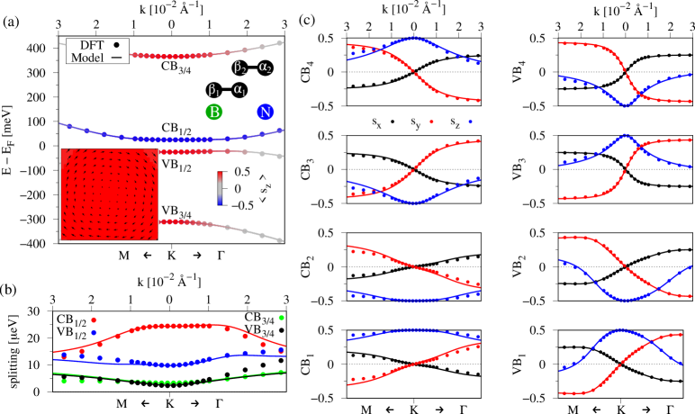
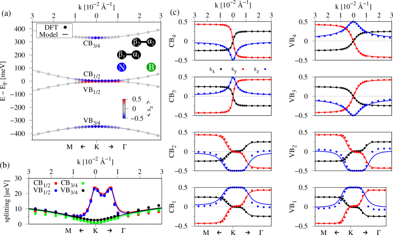
In the case of hBN/BLG structures, we follow a similar fitting strategy as before. Focusing on band energies only, the orbital parameters are determined first. Then, we fix the intrinsic SOC parameters, combining the knowledge about pristine graphene Gmitra et al. (2009), pristine BLG Konschuh et al. (2012), and graphene/hBN heterostructures Zollner et al. (2019). For example, in the (Bh2,H) stacking, and assuming that the hBN layer has no impact on the top graphene layer, we fix the intrinsic SOC parameter for () to about eV (eV), according to Ref. Konschuh et al. (2012), and with the knowledge about the eV difference between dimer/non-dimer atoms. The intrinsic SOC parameters of the lower graphene layer are proximity modified by the hBN Zollner et al. (2019). For this particular graphene/hBN stacking, the atom () would have an intrinsic SOC of about eV (eV). Since is still a dimer atom within BLG, we have to reduce the value additionally by eV, while is fixed by the previous consideration. Finally, we fit for the remaining SOC parameters that best reproduce the band splittings and spin expectation values, taking also into account the previously determined intrinsic Rashba SOC of pristine BLG and the Rashba SOC in graphene/hBN heterostructures Zollner et al. (2019). For example, the lower graphene layer in the (Bh2,H) stacking, acquires a Rashba SOC of eV (eV) from the upper graphene (lower hBN) layer, resulting in eV. Following this procedure, we can quite accurately reproduce the dispersion, spin splittings, and spin expectation values of the three hBN/BLG heterostructure stackings we consider, see Fig. 4, Fig. 5, and Fig. 6. The model parameters are summarized in Table 3. The remaining discrepancies between the model and the DFT results arise due to the influence of hBN orbitals, disturbing the effective -orbital-based model description of BLG, similar as in graphene/hBN heterostructures Zollner et al. (2019).
Focusing on the energetically most favorable (Bh2,H) stacking, see Fig. 4, we find a sizable orbital gap ( meV) at the Fermi level without external electric field. Remember that the layer and sublattice character plays an important role in the BLG dispersion Gmitra and Fabian (2017); Zollner et al. (2020); Zollner and Fabian (2021). The hBN layer introduces a significant potential difference between the graphene layers, opening the band gap. For this specific stacking, the low-energy valence bands, VB1/2, are formed by the bottom graphene layer, being in direct contact to hBN. More specifically, it is the non-dimer atom forming these bands. In contrast, the non-dimer atom forms the low-energy conduction bands, CB1/2. The low-energy valence (conduction) band is spin split by about eV (eV). The reason for this difference in the splitting is due to short-range proximity effect. The intrinsic SOC parameter of (eV) is proximity-modified due to the subjacent hBN layer, while the intrinsic SOC parameter of (eV) stays intact. The vortex-like spin-texture of the low-energy bands, which is due to the Rashba SOC, is visualized in the inset of Fig. 4(a) as an exemplary case.
The high-energy bands, being far away from the Fermi level, are formed by dimer atoms and . Moreover, the asymmetry is strongly affected by the hBN layer, see Table 3.
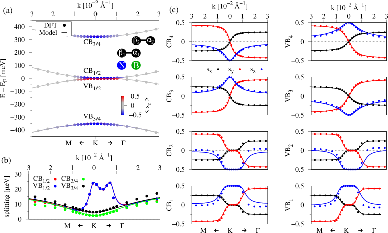
The low-energy dispersions and spin splittings of the other stackings, see Fig. 5 for (Nh2,H) and Fig. 6 for (Nh2,B), are markedly different to the (Bh2,H) stacking. First, we find that the orbital gap is nearly closed. This cannot be seen on the chosen energy scale, but the gap is about , as we have found above. In addition, the low-energy band splittings are nearly equal. The reason is that the hBN layer, for these two stackings, does not alter the intrinsic SOC parameter of as much as before. In conclusion, the low-energy band properties of BLG are mainly influenced by hBN in terms of the orbital band gap, while SOC parameters stay on the order of few to tens of eV. The atomic stacking configuration strongly influences the size of the band gap, which can range from few to tens of meV.
Applying an external electric field essentially adds to the internal field, that arises due the asymmetry introduced by the hBN layer. For example, in the (Bh2,H) stacking, an external electric field of 1 V/nm tunes the parameter from about to meV. In other words, the band character of the low-energy bands has switched, and now the valence (conduction) bands are formed by (). In addition, since the intrinsic SOC parameters of these atoms do not change with applied field, the band splittings are also switched accordingly. This electric field induced switching of the low-energy spin splittings resembles the spin-orbit and exchange valve effects as in Refs. Gmitra and Fabian (2017); Zollner et al. (2018); Zollner and Fabian (2021) for BLG heterostructures. For a certain external field value, one can even fully counter the internal field and close the gap. In addition, the Rashba SOC parameters are affected by the field, which are roughly tunable by eV per V/nm. Otherwise, all other orbital and spin-orbit parameters are barely affected by the external electric field. The model parameters with electric field are also summarized in Table 3.
IV.3 hBN encapsulated BLG
In a similar way as for the hBN/BLG heterostructures, we fit the band properties of the hBN encapsulated BLG structures. First, we determine the orbital parameters from the band energies only. The intrinsic SOC parameters are again fixed according to Ref. Zollner et al. (2019) for the different stacking configurations of the individual top and bottom graphene/hBN bilayers within the heterostructures and from the dimer/non-dimer difference discussed above. Then, we fit for the remaining SOC parameters that best reproduce the band splittings and spin expectation values, again taking into account the argumentation for the Rashba SOCs. The fit results are summarized in Table 4.
| system | (Bh2N,HH) | (Nh2B,HH) | (Bh2B,HH) | (Bh2H,HB) | (Nh2H,HB) | (Nh2H,BB) |
|---|---|---|---|---|---|---|
| [eV] | 2.563 (2.561) | 2.527 (2.526) | 2.570 (2.565) | 2.567 (2.562) | 2.517 (2.511) | 2.506 (2.505) |
| [eV] | 0.337 (0.337) | 0.337 (0.337) | 0.337 (0.336) | 0.335 (0.335) | 0.335 (0.335) | 0.334 (0.333) |
| [eV] | 0.266 (0.266) | 0.271 (0.273) | 0.269 (0.272) | 0.268 (0.273) | 0.273 (0.276) | 0.273 (0.274) |
| [eV] | -0.151 (-0.152) | -0.150 (-0.150) | -0.149 (-0.150) | -0.148 (-0.150) | -0.149 (-0.149) | -0.149 (-0.150) |
| [meV] | 0 (-1.185) | 0 (-1.350) | -17.980 (-24.685) | -17.215 (-23.853) | 0.146 (-1.178) | 0 (-1.319) |
| [meV] | 45.137 (45.020) | -25.810 (-24.997) | 9.649 (9.517) | 2.285 (2.186) | -33.176 (-32.334) | -40.526 (-39.781) |
| [eV] | 4.0 (4.4) | 6.0 (6.6) | 2.5 (2.9) | 1.5 (2.0) | 2.5 (2.9) | 10.2 (10.2) |
| [eV] | -4.0 (-3.6) | -6.0 (-6.1) | -6.6 (-5.6) | -9.3 (-8.4) | -7.6 (-7.2) | -10.2 (-10.3) |
| [eV] | 7.4 (7.4) | 12.0 (12.0) | 7.4 (7.4) | 7.4 (7.4) | 12.0 (12.0) | 13.8 (13.8) |
| [eV] | 4.9 (4.9) | 11.8 (11.8) | 4.9 (4.9) | 4.9 (4.9) | 11.8 (11.8) | 12.2 (12.2) |
| [eV] | 4.9 (4.9) | 11.8 (11.8) | 11.8 (11.8) | 12.2 (12.2) | 12.2 (12.2) | 12.2 (12.2) |
| [eV] | 7.4 (7.4) | 12.0 (12.0) | 12.0 (12.0) | 13.8 (13.8) | 13.8 (13.8) | 13.8 (13.8) |
| [eV] | 22.0 (21.9) | 11.8 (14.3) | 12.0 (11.8) | 11.0 (11.6) | 24.2 (20.7) | 15.0 (13.8) |
| [eV] | 22.0 (22.5) | 11.8 (15.5) | 17.4 (17.6) | 17.2 (17.4) | 27.2 (23.7) | 15.0 (14.0) |
For the hBN encapsulated BLG heterostructures, inversion symmetry can be restored for special stacking configurations. For example, in the (Bh2N,HH) stacking and considering surrounding hBN monolayers, we find that the potential difference , just as for pristine BLG without external electric field. In contrast to pristine BLG, the asymmetry is strongly modified due to the hBN layers. Moreover, also the SOC parameters are heavily influenced. In particular, the Rashba SOCs have the opposite sign and nearly the same magnitude compared to pristine BLG. The intrinsic SOC parameters are again symmetric (, ), but reduced in value due to the hBN layers. Remarkably, the parameters are significantly enhanced compared to pristine BLG. Similarly, the (Nh2B,HH) and (Nh2H,BB) stacking configurations also have inversion symmetry and the band gap closes.
Once we employ top monolayer hBN and bottom bilayer hBN for the encapsulation, inversion symmetry is again broken for all stackings, and a finite arises. However, the effect of adding a second hBN layer is not dramatic anymore. For example, the (Bh2N,HH) stacking shows a potential difference of meV due to the additional hBN layer, while SOC parameters are barely affected anymore. From that, we conclude that only the neighboring hBN layers have a strong impact on the spin physics in BLG. Nevertheless, the exact encapsulation can drastically influence the low-energy bands.
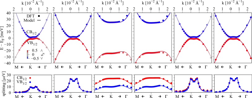
In Fig. 7, we show the low-energy bands and corresponding spin splittings for the different stacking configurations with top monolayer and bottom bilayer hBN. Again, we see very good agreement of DFT and model results, giving us further confidence in our model Hamiltonian and the fitted parameters. We find band gaps in the range of 0 to 50 meV for the different structures. Experimentally, when a moiré pattern is present, one can therefore expect local variations in the band gap, due to the different atomic stackings.
IV.4 Gate tunability
| Field [V/nm] | -2.0 | -1.5 | -1.0 | -0.75 | -0.5 | -0.25 | 0.0 | 0.25 | 0.5 | 0.75 | 1.0 | 1.5 | 2.0 |
|---|---|---|---|---|---|---|---|---|---|---|---|---|---|
| [eV] | 2.558 | 2.558 | 2.559 | 2.559 | 2.559 | 2.559 | 2.561 | 2.560 | 2.559 | 2.558 | 2.558 | 2.558 | 2.557 |
| [eV] | 0.336 | 0.336 | 0.337 | 0.337 | 0.337 | 0.337 | 0.337 | 0.337 | 0.337 | 0.337 | 0.337 | 0.336 | 0.336 |
| [eV] | 0.319 | 0.296 | 0.278 | 0.272 | 0.268 | 0.266 | 0.266 | 0.266 | 0.266 | 0.269 | 0.273 | 0.290 | 0.311 |
| [eV] | -0.151 | -0.151 | -0.152 | -0.152 | -0.152 | -0.152 | -0.152 | -0.152 | -0.152 | -0.152 | -0.152 | -0.152 | -0.151 |
| gap [meV] | 178.752 | 144.873 | 100.845 | 74.937 | 46.745 | 17.251 | 1.362 | 2.624 | 22.831 | 52.152 | 80.038 | 128.363 | 166.330 |
| [meV] | -120.184 | -89.450 | -57.897 | -41.892 | -25.796 | -9.664 | -1.185 | 1.854 | 12.664 | 28.816 | 44.906 | 76.747 | 107.89 |
| [meV] | 45.533 | 45.331 | 45.179 | 45.121 | 45.076 | 45.042 | 45.020 | 45.009 | 45.010 | 45.022 | 45.044 | 45.119 | 45.228 |
| [eV] | 14.5 | 11.6 | 9.0 | 7.5 | 6.4 | 5.0 | 4.4 | 3.0 | 2.2 | 0.7 | -0.8 | -4.3 | -7.7 |
| [eV] | 9.8 | 6.6 | 3.1 | 1.6 | -0.3 | -2.0 | -3.6 | -4.2 | -5.8 | -7.3 | -8.9 | -11.6 | -14.4 |
| [eV] | 7.4 | 7.4 | 7.4 | 7.4 | 7.4 | 7.4 | 7.4 | 7.4 | 7.4 | 7.4 | 7.4 | 7.4 | 7.4 |
| [eV] | 4.9 | 4.9 | 4.9 | 4.9 | 4.9 | 4.9 | 4.9 | 4.9 | 4.9 | 4.9 | 4.9 | 4.9 | 4.9 |
| [eV] | 4.9 | 4.9 | 4.9 | 4.9 | 4.9 | 4.9 | 4.9 | 4.9 | 4.9 | 4.9 | 4.9 | 4.9 | 4.9 |
| [eV] | 7.4 | 7.4 | 7.4 | 7.4 | 7.4 | 7.4 | 7.4 | 7.4 | 7.4 | 7.4 | 7.4 | 7.4 | 7.4 |
| [eV] | 25.8 | 23.9 | 22.6 | 22.4 | 22.3 | 22.4 | 21.9 | 23.2 | 23.6 | 24.3 | 25.1 | 26.4 | 28.1 |
| [eV] | 26.9 | 25.3 | 24.5 | 24.0 | 23.7 | 23.3 | 22.5 | 23.8 | 23.1 | 22.9 | 22.8 | 23.4 | 25.0 |
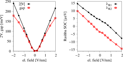
In the following, we consider the energetically most favorable structure of hBN-encapsulated BLG and again study the electric field tunability. In particular, we consider the structure with top monolayer hBN and bottom bilayer hBN in the (Bh2N,HH) stacking configuration. The fit results as function of the external electric field are summarized in Table 5.
In Fig. 8, we show the evolution of the potential , the band gap, and the two Rashba parameters and as function of the applied electric field, similar as above for pristine BLG. Both Rashba couplings again follow a linear trend, with a tunability of about eV per V/nm. This value is a bit larger compared to pristine BLG, but still of the same magnitude. The potential parameter shows a nonlinear onset for small electric fields, and a linear tunability for higher electric fields. For small electric fields, the band gap also closely follows and starts to drastically deviate for fields above 1 V/nm. The asymmetry for small electric field values originates from the structural asymmetry.
V Twist Angle Dependent Band Gap
So far, we have considered specific stacking configurations to get a quantitative and qualitative feeling for orbital and spin-orbit properties. However, this only provides a glimpse of local regions in a generic experimental setup. In fact, in realistic macroscopic experimental samples, stacking faults and disorder can be present Warner et al. (2009); Wilson et al. (2020). Even with the knowledge about the stacking dependent electronic spectra we have analyzed above, the interpretation of experimental data is further complicated. Here, we do not consider lateral disorder (stacking faults) within BLG, which may change electronic states.
Instead, we consider twisted Bernal-BLG/hBN heterostructures, where essentially several of the investigated stacking configurations are present simultaneously. Since these structures can become quite large and are computationally very demanding, we employ the plane wave based DFT code Quantum Espresso Giannozzi et al. (2009) and neglect the effects of SOC. The above analysis has already shown that SOC effects are much smaller than orbital ones, making this a valid approach. In any case, the plane wave and pseudopotential method, implemented in Quantum Espresso, cannot give correct spin-orbit splittings in graphene, since the relevant -orbitals are missing Gmitra et al. (2009); Konschuh et al. (2010). Nevertheless, on an orbital level, the dispersions are the same as calculated with WIEN2k, and we can safely study the electric field tunability.
The twisted heterostructures were set-up with the atomic simulation environment (ASE) Bahn and Jacobsen (2002) and the CellMatch code Lazic (2015), implementing the coincidence lattice method Koda et al. (2016); Carr et al. (2020). We keep the lattice constant of BLG fixed at Å and strain hBN less than %. In particular, we consider 4 different twisted BLG/hBN structures, with twist angles between hBN and BLG of (468 atoms, Å), (166 atoms, Å), (374 atoms, Å), and (468 atoms, Å), where is the lattice constant of the twisted supercell. We use an energy cutoff for charge density of Ry and the kinetic energy cutoff for wavefunctions is Ry for the scalar relativistic pseudopotentials with the projector augmented wave method Kresse and Joubert (1999) with the Perdew-Burke-Ernzerhof exchange correlation functional Perdew et al. (1996). Self-consistent calculations are carried out with a -point sampling of . Again, we employ DFT-D2 vdW corrections Grimme (2006); Grimme et al. (2010); Barone et al. (2009). In order to simulate quasi-2D systems, we add a vacuum of about Å to avoid interactions between periodic images in our slab geometry. To get proper interlayer distances and to capture possible moiré reconstructions, we allow all atoms to move freely within the heterostructure geometry during relaxation. Relaxation is performed until every component of each force is reduced below [Ry/], where is the Bohr radius.
After relaxation, we calculate the mean interlayer distances, and , and the standard deviations, , from the coordinates of the C, B, and N atoms. The standard deviations represent the amount of rippling of the hBN layer. From the calculated band energies, we extract the global band gap. All these results are listed in Table 6. We find relaxed interlayer distances of 3.24 Å, between the graphene layers, and 3.26 Å, between the graphene and hBN layers. These values are in agreement with earlier calculations Giovannetti et al. (2007); Zollner et al. (2019). The global band gap increases linearly with the twist angle. Fitting the twisted band gap data to a linear function, we find a global band gap of 23.23 meV and a slope of 0.39 meV/∘.
In general, the global band gap results from the average of the band gaps of the different local stacking configurations. Therefore, we also consider the high-symmetry stackings from above, which correspond to and twist angles and fix the interlayer distances of 3.24 Å, between the graphene layers, and 3.26 Å, between the graphene and hBN layers, which are the average of the twisted structures. From the band gaps of the individual stackings, see Table 7, we can also calculate the average gap, which we determine to be 25.82 meV, in good agreement with the extrapolated one of the twisted structures.
| [°] | [Å] | [Å] | [pm] | gap [meV] |
|---|---|---|---|---|
| 6.42 | 3.2379 | 3.2637 | 3.9260 | 25.58 |
| 10.89 | 3.2396 | 3.2606 | 2.3575 | 27.50 |
| 14.56 | 3.2385 | 3.2562 | 1.4732 | 29.16 |
| 19.59 | 3.2448 | 3.2608 | 0.5418 | 30.63 |
| stacking | E-E0 [meV] | gap [meV] |
|---|---|---|
| (Bh2,H) | 0 | 46.48 |
| (Nh2,H) | 22.62 | 11.38 |
| (Nh2,B) | 30.36 | 11.77 |
| (Bh2,N) | 29.35 | 53.43 |
| (Hh2,N) | 21.80 | 18.63 |
| (Hh2,B) | 0.15 | 13.22 |
| average | - | 25.82 |
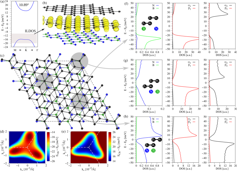
In order to emphasize the local band gap variation, we considered the smallest twisted BLG/hBN structure with a twist angle of as an exemplary case, for which we have calculated the integrated local density of states (ILDOS) for the valence band edge states, see Fig. 9(a,b). The valence band edge is formed by the non-dimer atoms of the lower graphene layer in direct contact with the hBN, which is nicely reflected in the real-space picture of the ILDOS. At first glance, one may think that all the relevant non-dimer C atoms contribute equally. However, within the twisted structure, see Fig. 9(c), one can identify local high-symmetry stacking configurations, which provide very different band gaps and DOS contributions, see Fig. 9(f-h). In other words, by having knowledge about local high-symmetry stackings, one can map the local band gaps to the twisted heterostructures. Looking at the band edge energies in the vicinity of the K point, see Fig. 9(d,e), also the trigonal warping can be seen McCann and Koshino (2013); Konschuh et al. (2012). Moreover, the trigonal warping points are no longer directed along high-symmetry lines due to the twist angle. This is also the reason, why we extracted the band gaps for the twisted structures from the band edge extrema around the K point, see Fig. 9(d,e), and not from the dispersion along the high-symmetry lines, see Fig. 9(a).
VI Summary
In summary, we have calculated the electronic structures of hBN encapsulated BLG from first principles. By employing a model Hamiltonian, we were able to reproduce the relevant low-energy bands of BLG using reasonable fit parameters. The main effect of hBN on the BLG dispersion is on the orbital level, introducing band gaps up to tens of meV, depending on the stacking and encapsulation scenario. Additionally, while SOC parameters stay in the range of few to tens of eV, they are markedly proximity modified by the surrounding hBN layer(s). Further tunability, mainly of the orbital gap and the layer-resolved Rashba SOCs, is provided by a transverse electric field. From the investigated twisted BLG/hBN heterostructures, we find that rather large band gap variations arise from the different local stacking configurations.
The modulation of the band gap due to different stacking configurations occurs on a spatial scale on the order of nanometers. Such precise spatial resolution can be achieved, for example, by scanning tunneling microscopy (STM), which have been used to characterize BLG on hBN Yankowitz et al. (2014); Holdman et al. (2019). In contrast, STM measurements require the BLG to be exposed without encapsulation in hBN. This exposure can lead to contamination and unintentional doping of the top BLG layer, obscuring the impact of diverse stacking orders on the band structure due to variations in disorder potential. Furthermore, the absence of metallic or graphite bottom gates can result in further interference from the substrate. Another potential experiment with sufficient spatial resolution could be scanning gate microscopy, which furthermore allows encapsulation of the BLG in hBN. Yet, previous measurements on dual-gated BLG were influenced by localized states Gold et al. (2020) that might also mask the variations in the band gap across the sample. While transport spectroscopy Overweg et al. (2018); Icking et al. (2022) or optical experiments Mak et al. (2009); Kuzmenko et al. (2009); Zhang et al. (2009) can determine the band gap in BLG, they yield an averaged gap across the sample due to factors like the laser beam spot size. Still, they could be utilized to study the effect of different twist angles between the hBN and BLG on the effective band gap.
The sensitivity of stacking configuration related spatial band gap variations to external parameters such as strain, interface disorder, or unintentional doping, necessitates samples of exceptionally high quality, particularly relying on state-of-the-art graphite-gated BLG devices. The presented results should be particularly helpful in understanding and analyzing spectra of BLG quantum point contacts Banszerus et al. (2020); Lee et al. (2020) and quantum dots Knothe and Fal’ko (2020); Möller et al. (2021, 2023); Eich et al. (2018) for building moiré potentials to realistically model orbital and spin-orbit effects in extended geometries.
Acknowledgements.
This work was funded by the European Union Horizon 2020 Research and Innovation Program under contract number 881603 (Graphene Flagship), Deutsche Forschungsgemeinschaft (DFG, German Research Foundation) SFB 1277 (Project No. 314695032), and DFG SPP 2244 (Project No. 443416183).References
- Cai et al. (2018) Xingke Cai, Yuting Luo, Bilu Liu, and Hui-Ming Cheng, “Preparation of 2d material dispersions and their applications,” Chem. Soc. Rev. 47, 6224–6266 (2018).
- Kumar et al. (2020) Prateek Kumar, Maneesha Gupta, and Kunwar Singh, “Performance evaluation of transition metal dichalcogenides based steep subthreshold slope tunnel field effect transistor,” Silicon 12, 1857–1864 (2020).
- Zhang et al. (2019a) Wen Zhang, Ping Kwan Johnny Wong, Rui Zhu, and Andrew T S Wee, “Van der Waals magnets: Wonder building blocks for two‐dimensional spintronics?” InfoMat 1, 479 (2019a).
- Gong and Zhang (2019) Cheng Gong and Xiang Zhang, “Two-dimensional magnetic crystals and emergent heterostructure devices,” Science 363, eaav4450 (2019).
- Li et al. (2019) Hui Li, Shuangchen Ruan, and Yu‐Jia Zeng, “Intrinsic Van Der Waals Magnetic Materials from Bulk to the 2D Limit: New Frontiers of Spintronics,” Adv. Mater. 31, 1900065 (2019).
- Song et al. (2018) Tiancheng Song, Xinghan Cai, Matisse Wei-Yuan Tu, Xiaoou Zhang, Bevin Huang, Nathan P. Wilson, Kyle L. Seyler, Lin Zhu, Takashi Taniguchi, Kenji Watanabe, Michael A. McGuire, David H. Cobden, Di Xiao, Wang Yao, and Xiaodong Xu, “Giant tunneling magnetoresistance in spin-filter van der Waals heterostructures,” Science 360, 1214 (2018).
- Sierra et al. (2021) Juan F Sierra, Jaroslav Fabian, Roland K Kawakami, Stephan Roche, and Sergio O Valenzuela, “Van der waals heterostructures for spintronics and opto-spintronics,” Nature Nanotechnology , 1–13 (2021).
- McCann (2006) Edward McCann, “Asymmetry gap in the electronic band structure of bilayer graphene,” Phys. Rev. B 74, 161403– (2006).
- Min et al. (2007) Hongki Min, Bhagawan Sahu, Sanjay K. Banerjee, and A. H. MacDonald, “Ab initio theory of gate induced gaps in graphene bilayers,” Phys. Rev. B 75, 155115 (2007).
- McCann and Koshino (2013) Edward McCann and Mikito Koshino, “The electronic properties of bilayer graphene,” Rep. Prog. Phys. 76, 056503 (2013).
- Slizovskiy et al. (2021) S. Slizovskiy, A. Garcia-Ruiz, A. I. Berdyugin, N. Xin, T. Taniguchi, K. Watanabe, A. K. Geim, N. D. Drummond, and V. I. Fal’ko, “Out-of-Plane Dielectric Susceptibility of Graphene in Twistronic and Bernal Bilayers,” Nano Lett. 21, 6678–6683 (2021).
- Ohta et al. (2006) Taisuke Ohta, Aaron Bostwick, Thomas Seyller, Karsten Horn, and Eli Rotenberg, “Controlling the electronic structure of bilayer graphene,” Science 313, 951–954 (2006).
- Zhou et al. (2007) S. Y. Zhou, G.-H. Gweon, A. V. Fedorov, P. N. First, W. A. de Heer, D.-H. Lee, F. Guinea, A. H. Castro Neto, and A. Lanzara, “Substrate-induced bandgap opening in epitaxial graphene,” Nat. Mater. 6, 770–775 (2007).
- Oostinga et al. (2007) Jeroen B. Oostinga, Hubert B. Heersche, Xinglan Liu, Alberto F. Morpurgo, and Lieven M. K. Vandersypen, “Gate-induced insulating state in bilayer graphene devices,” Nat. Mater. 7, 151–157 (2007).
- Mak et al. (2009) Kin Fai Mak, Chun Hung Lui, Jie Shan, and Tony F. Heinz, “Observation of an electric-field-induced band gap in bilayer graphene by infrared spectroscopy,” Phys. Rev. Lett. 102, 256405 (2009).
- Icking et al. (2022) Eike Icking, Luca Banszerus, Frederike Wörtche, Frank Volmer, Philipp Schmidt, Corinne Steiner, Stephan Engels, Jonas Hesselmann, Matthias Goldsche, Kenji Watanabe, Takashi Taniguchi, Christian Volk, Bernd Beschoten, and Christoph Stampfer, “Transport spectroscopy of ultraclean tunable band gaps in bilayer graphene,” Advanced Electronic Materials 8, 2200510 (2022).
- Zhou et al. (2022) Haoxin Zhou, Ludwig Holleis, Yu Saito, Liam Cohen, William Huynh, Caitlin L. Patterson, Fangyuan Yang, Takashi Taniguchi, Kenji Watanabe, and Andrea F. Young, “Isospin magnetism and spin-polarized superconductivity in bernal bilayer graphene,” Science 375, 774–778 (2022).
- de la Barrera et al. (2022) Sergio C. de la Barrera, Samuel Aronson, Zhiren Zheng, Kenji Watanabe, Takashi Taniguchi, Qiong Ma, Pablo Jarillo-Herrero, and Raymond Ashoori, “Cascade of isospin phase transitions in bernal-stacked bilayer graphene at zero magnetic field,” Nature Physics 18, 771–775 (2022).
- Weitz et al. (2010) R. T. Weitz, M. T. Allen, B. E. Feldman, J. Martin, and A. Yacoby, “Broken-symmetry states in doubly gated suspended bilayer graphene,” Science 330, 812–816 (2010).
- Geisenhof et al. (2021) Fabian R. Geisenhof, Felix Winterer, Anna M. Seiler, Jakob Lenz, Tianyi Xu, Fan Zhang, and R. Thomas Weitz, “Quantum anomalous hall octet driven by orbital magnetism in bilayer graphene,” Nature 598, 53–58 (2021).
- Kou et al. (2014) A. Kou, B. E. Feldman, A. J. Levin, B. I. Halperin, K. Watanabe, T. Taniguchi, and A. Yacoby, “Electron-hole asymmetric integer and fractional quantum hall effect in bilayer graphene,” Science 345, 55–57 (2014).
- Ki et al. (2014) Dong-Keun Ki, Vladimir I. Fal’ko, Dmitry A. Abanin, and Alberto F. Morpurgo, “Observation of even denominator fractional quantum hall effect in suspended bilayer graphene,” Nano Letters 14, 2135–2139 (2014).
- Zheng et al. (2020) Zhiren Zheng, Qiong Ma, Zhen Bi, Sergio de la Barrera, Ming-Hao Liu, Nannan Mao, Yang Zhang, Natasha Kiper, Kenji Watanabe, Takashi Taniguchi, Jing Kong, William A. Tisdale, Ray Ashoori, Nuh Gedik, Liang Fu, Su-Yang Xu, and Pablo Jarillo-Herrero, “Unconventional ferroelectricity in moiré heterostructures,” Nature 588, 71–76 (2020).
- Seiler et al. (2022) Anna M. Seiler, Fabian R. Geisenhof, Felix Winterer, Kenji Watanabe, Takashi Taniguchi, Tianyi Xu, Fan Zhang, and R. Thomas Weitz, “Quantum cascade of correlated phases in trigonally warped bilayer graphene,” Nature 608, 298–302 (2022).
- Kane and Mele (2005) C. L. Kane and E. J. Mele, “Quantum spin hall effect in graphene,” Phys. Rev. Lett. 95, 226801 (2005).
- Konschuh et al. (2012) S. Konschuh, M. Gmitra, D. Kochan, and J. Fabian, “Theory of spin-orbit coupling in bilayer graphene,” Phys. Rev. B 85, 115423 (2012).
- Kurzmann et al. (2021) Annika Kurzmann, Yaakov Kleeorin, Chuyao Tong, Rebekka Garreis, Angelika Knothe, Marius Eich, Christopher Mittag, Carolin Gold, Folkert Kornelis de Vries, Kenji Watanabe, Takashi Taniguchi, Vladimir Fal’ko, Yigal Meir, Thomas Ihn, and Klaus Ensslin, “Kondo effect and spin–orbit coupling in graphene quantum dots,” Nature Communications 12, 6004 (2021).
- Banszerus et al. (2021) L. Banszerus, S. Möller, C. Steiner, E. Icking, S. Trellenkamp, F. Lentz, K. Watanabe, T. Taniguchi, C. Volk, and C. Stampfer, “Spin-valley coupling in single-electron bilayer graphene quantum dots,” Nature Communications 12, 5250 (2021).
- Wojtaszek et al. (2014) M. Wojtaszek, I. J. Vera-Marun, E. Whiteway, M. Hilke, and B. J. van Wees, “Absence of hyperfine effects in 13c-graphene spin-valve devices,” Phys. Rev. B 89, 035417 (2014).
- Fischer and Loss (2009) Jan Fischer and Daniel Loss, “Dealing with decoherence,” Science 324, 1277–1278 (2009).
- Overweg et al. (2018) Hiske Overweg, Hannah Eggimann, Xi Chen, Sergey Slizovskiy, Marius Eich, Riccardo Pisoni, Yongjin Lee, Peter Rickhaus, Kenji Watanabe, Takashi Taniguchi, Vladimir Fal’ko, Thomas Ihn, and Klaus Ensslin, “Electrostatically Induced Quantum Point Contacts in Bilayer Graphene,” Nano Lett. 18, 553–559 (2018).
- Eich et al. (2018) Marius Eich, Riccardo Pisoni, Alessia Pally, Hiske Overweg, Annika Kurzmann, Yongjin Lee, Peter Rickhaus, Kenji Watanabe, Takashi Taniguchi, Klaus Ensslin, and Thomas Ihn, “Coupled Quantum Dots in Bilayer Graphene,” Nano Lett. 18, 5042–5048 (2018).
- Banszerus et al. (2020) L. Banszerus, B. Frohn, T. Fabian, S. Somanchi, A. Epping, M. Müller, D. Neumaier, K. Watanabe, T. Taniguchi, F. Libisch, B. Beschoten, F. Hassler, and C. Stampfer, “Observation of the Spin-Orbit Gap in Bilayer Graphene by One-Dimensional Ballistic Transport,” Phys. Rev. Lett. 124, 177701 (2020).
- Garreis et al. (2021) R. Garreis, A. Knothe, C. Tong, M. Eich, C. Gold, K. Watanabe, T. Taniguchi, V. Fal’ko, T. Ihn, K. Ensslin, and A. Kurzmann, “Shell filling and trigonal warping in graphene quantum dots,” Phys. Rev. Lett. 126, 147703 (2021).
- Lee et al. (2020) Yongjin Lee, Angelika Knothe, Hiske Overweg, Marius Eich, Carolin Gold, Annika Kurzmann, Veronika Klasovika, Takashi Taniguchi, Kenji Wantanabe, Vladimir Fal’ko, Thomas Ihn, Klaus Ensslin, and Peter Rickhaus, “Tunable valley splitting due to topological orbital magnetic moment in bilayer graphene quantum point contacts,” Phys. Rev. Lett. 124, 126802 (2020).
- Banszerus et al. (2023) Luca Banszerus, Samuel Möller, Katrin Hecker, Eike Icking, Kenji Watanabe, Takashi Taniguchi, Fabian Hassler, Christian Volk, and Christoph Stampfer, “Particle-hole symmetry protects spin-valley blockade in graphene quantum dots,” (2023).
- Zutic et al. (2019) Igor Zutic, Alex Matos-Abiague, Benedikt Scharf, Hanan Dery, and Kirill Belashchenko, “Proximitized materials,” Mater. Today 22, 85 (2019).
- Zollner et al. (2018) Klaus Zollner, Martin Gmitra, and Jaroslav Fabian, “Electrically tunable exchange splitting in bilayer graphene on monolayer Cr2X2Te6 with X = Ge, Si, and Sn,” New J. Phys. 20, 073007 (2018).
- Zollner et al. (2019) Klaus Zollner, Martin Gmitra, and Jaroslav Fabian, “Heterostructures of graphene and hBN: Electronic, spin-orbit, and spin relaxation properties from first principles,” Phys. Rev. B 99, 125151 (2019).
- Zollner et al. (2020) Klaus Zollner, Martin Gmitra, and Jaroslav Fabian, “Swapping exchange and spin-orbit coupling in 2d van der waals heterostructures,” Phys. Rev. Lett. 125, 196402 (2020).
- Zollner and Fabian (2019) Klaus Zollner and Jaroslav Fabian, “Single and bilayer graphene on the topological insulator : Electronic and spin-orbit properties from first principles,” Phys. Rev. B 100, 165141 (2019).
- Omar et al. (2019) S. Omar, B. N. Madhushankar, and B. J. van Wees, “Large spin-relaxation anisotropy in bilayer-graphene/ heterostructures,” Phys. Rev. B 100, 155415 (2019).
- Bisswanger et al. (2022) Timo Bisswanger, Zachary Winter, Anne Schmidt, Frank Volmer, Kenji Watanabe, Takashi Taniguchi, Christoph Stampfer, and Bernd Beschoten, “Cvd bilayer graphene spin valves with 26 m spin diffusion length at room temperature,” Nano Letters 22, 4949–4955 (2022).
- Gmitra and Fabian (2017) Martin Gmitra and Jaroslav Fabian, “Proximity Effects in Bilayer Graphene on Monolayer WSe2: Field-Effect Spin Valley Locking, Spin-Orbit Valve, and Spin Transistor,” Phys. Rev. Lett. 119, 146401 (2017).
- Island et al. (2019) J. O. Island, X. Cui, C. Lewandowski, J. Y. Khoo, E. M. Spanton, H. Zhou, D. Rhodes, J. C. Hone, T. Taniguchi, K. Watanabe, L. S. Levitov, M. P. Zaletel, and A. F. Young, “Spin-orbit-driven band inversion in bilayer graphene by the van der Waals proximity effect,” Nature 571, 85 (2019).
- Zhang et al. (2023) Yiran Zhang, Robert Polski, Alex Thomson, Étienne Lantagne-Hurtubise, Cyprian Lewandowski, Haoxin Zhou, Kenji Watanabe, Takashi Taniguchi, Jason Alicea, and Stevan Nadj-Perge, “Enhanced superconductivity in spin–orbit proximitized bilayer graphene,” Nature 613, 268–273 (2023).
- Li et al. (2020a) Jing Li, Han-Bing Leng, Hailong Fu, Kenji Watanabe, Takashi Taniguchi, Xin Liu, Chao-Xing Liu, and Jun Zhu, “Superconducting proximity effect in a transparent van der waals superconductor-metal junction,” Phys. Rev. B 101, 195405 (2020a).
- Moriya et al. (2020) Rai Moriya, Naoto Yabuki, and Tomoki Machida, “Superconducting proximity effect in a van der waals junction,” Phys. Rev. B 101, 054503 (2020).
- Zollner et al. (2016) Klaus Zollner, Martin Gmitra, Tobias Frank, and Jaroslav Fabian, “Theory of proximity-induced exchange coupling in graphene on hBN/(Co, Ni),” Phys. Rev. B 94, 155441 (2016).
- Zollner and Fabian (2021) Klaus Zollner and Jaroslav Fabian, “Bilayer graphene encapsulated within monolayers of or : Tunable proximity spin-orbit or exchange coupling,” Phys. Rev. B 104, 075126 (2021).
- Dean et al. (2010) C. R. Dean, A. F. Young, I. Meric, C. Lee, L. Wang, S. Sorgenfrei, K. Watanabe, T. Taniguchi, P. Kim, K. L. Shepard, and J. Hone, “Boron nitride substrates for high-quality graphene electronics,” Nature Nanotechnology 5, 722–726 (2010).
- Wang et al. (2013) L. Wang, I. Meric, P. Y. Huang, Q. Gao, Y. Gao, H. Tran, T. Taniguchi, K. Watanabe, L. M. Campos, D. A. Muller, J. Guo, P. Kim, J. Hone, K. L. Shepard, and C. R. Dean, “One-Dimensional Electrical Contact to a Two-Dimensional Material,” Science 342, 614–617 (2013).
- Watanabe et al. (2004) Kenji Watanabe, Takashi Taniguchi, and Hisao Kanda, “Direct-bandgap properties and evidence for ultraviolet lasing of hexagonal boron nitride single crystal,” Nature Materials 3, 404–409 (2004).
- Lindsay and Broido (2011) L. Lindsay and D. A. Broido, “Enhanced thermal conductivity and isotope effect in single-layer hexagonal boron nitride,” Phys. Rev. B 84, 155421 (2011).
- Yuan et al. (2019) Chao Yuan, Jiahan Li, Lucas Lindsay, David Cherns, James W. Pomeroy, Song Liu, James H. Edgar, and Martin Kuball, “Modulating the thermal conductivity in hexagonal boron nitride via controlled boron isotope concentration,” Communications Physics 2, 1–8 (2019).
- Banszerus et al. (2015) Luca Banszerus, Michael Schmitz, Stephan Engels, Jan Dauber, Martin Oellers, Federica Haupt, Kenji Watanabe, Takashi Taniguchi, Bernd Beschoten, and Christoph Stampfer, “Ultrahigh-mobility graphene devices from chemical vapor deposition on reusable copper,” Sci. Adv. 1, 1500222 (2015).
- Ajayi et al. (2017) Obafunso A Ajayi, Jenny V Ardelean, Gabriella D Shepard, Jue Wang, Abhinandan Antony, Takeshi Taniguchi, Kenji Watanabe, Tony F Heinz, Stefan Strauf, X-Y Zhu, and James C Hone, “Approaching the intrinsic photoluminescence linewidth in transition metal dichalcogenide monolayers,” 2D Materials 4, 031011 (2017).
- Raja et al. (2019) Archana Raja, Lutz Waldecker, Jonas Zipfel, Yeongsu Cho, Samuel Brem, Jonas D. Ziegler, Marvin Kulig, Takashi Taniguchi, Kenji Watanabe, Ermin Malic, Tony F. Heinz, Timothy C. Berkelbach, and Alexey Chernikov, “Dielectric disorder in two-dimensional materials,” Nature Nanotechnology 14, 832–837 (2019).
- Ersfeld et al. (2020) Manfred Ersfeld, Frank Volmer, Lars Rathmann, Luca Kotewitz, Maximilian Heithoff, Mark Lohmann, Bowen Yang, Kenji Watanabe, Takashi Taniguchi, Ludwig Bartels, Jing Shi, Christoph Stampfer, and Bernd Beschoten, “Unveiling valley lifetimes of free charge carriers in monolayer wse2,” Nano Letters 20, 3147–3154 (2020).
- Gao et al. (2016) Jian Gao, Baichang Li, Jiawei Tan, Phil Chow, Toh-Ming Lu, and Nikhil Koratkar, “Aging of transition metal dichalcogenide monolayers,” ACS Nano 10, 2628–2635 (2016).
- Gurram et al. (2018) M Gurram, S Omar, and B J van Wees, “Electrical spin injection, transport, and detection in graphene-hexagonal boron nitride van der waals heterostructures: progress and perspectives,” 2D Materials 5, 032004 (2018).
- Meng et al. (2018) Junhua Meng, Denggui Wang, Likun Cheng, Menglei Gao, and Xingwang Zhang, “Recent progress in synthesis, properties, and applications of hexagonal boron nitride-based heterostructures,” Nanotechnology 30, 074003 (2018).
- Maestre et al. (2021) Camille Maestre, Bérangère Toury, Philippe Steyer, Vincent Garnier, and Catherine Journet, “Hexagonal boron nitride: a review on selfstanding crystals synthesis towards 2d nanosheets,” Journal of Physics: Materials 4, 044018 (2021).
- Taniguchi and Watanabe (2007) T. Taniguchi and K. Watanabe, “Synthesis of high-purity boron nitride single crystals under high pressure by using ba–bn solvent,” Journal of Crystal Growth 303, 525–529 (2007).
- Zastrow (2019) Mark Zastrow, “Meet the crystal growers who sparked a revolution in graphene electronics,” Nature 572, 429–432 (2019).
- Onodera et al. (2019) Momoko Onodera, Kenji Watanabe, Miyako Isayama, Miho Arai, Satoru Masubuchi, Rai Moriya, Takashi Taniguchi, and Tomoki Machida, “Carbon-rich domain in hexagonal boron nitride: Carrier mobility degradation and anomalous bending of the landau fan diagram in adjacent graphene,” Nano Letters 19, 7282–7286 (2019).
- Onodera et al. (2020) Momoko Onodera, Takashi Taniguchi, Kenji Watanabe, Miyako Isayama, Satoru Masubuchi, Rai Moriya, and Tomoki Machida, “Hexagonal boron nitride synthesized at atmospheric pressure using metal alloy solvents: Evaluation as a substrate for 2d materials,” Nano Letters 20, 735–740 (2020).
- Kubota et al. (2007) Yoichi Kubota, Kenji Watanabe, Osamu Tsuda, and Takashi Taniguchi, “Deep ultraviolet light-emitting hexagonal boron nitride synthesized at atmospheric pressure,” Science 317, 932–934 (2007).
- Kubota et al. (2008) Yoichi Kubota, Kenji Watanabe, Osamu Tsuda, and Takashi Taniguchi, “Hexagonal boron nitride single crystal growth at atmospheric pressure using ni-cr solvent,” Chemistry of Materials 20, 1661–1663 (2008).
- Hoffman et al. (2014) T.B. Hoffman, B. Clubine, Y. Zhang, K. Snow, and J.H. Edgar, “Optimization of ni–cr flux growth for hexagonal boron nitride single crystals,” Journal of Crystal Growth 393, 114–118 (2014), the 19th American Conference on Crystal Growth and Epitaxy in conjunction with The 16th US Biennial Workshop on Organometallic Vapor Phase Epitaxy.
- Edgar et al. (2014) J.H. Edgar, T.B. Hoffman, B. Clubine, M. Currie, X.Z. Du, J.Y. Lin, and H.X. Jiang, “Characterization of bulk hexagonal boron nitride single crystals grown by the metal flux technique,” Journal of Crystal Growth 403, 110–113 (2014), 8th International Workshop on Bulk Nitrides Semiconductors (IWBNS VIII).
- Liu et al. (2018) Song Liu, Rui He, Lianjie Xue, Jiahan Li, Bin Liu, and James H. Edgar, “Single crystal growth of millimeter-sized monoisotopic hexagonal boron nitride,” Chemistry of Materials 30, 6222–6225 (2018).
- Li et al. (2020b) Jiahan Li, Christine Elias, Gaihua Ye, Dylan Evans, Song Liu, Rui He, Guillaume Cassabois, Bernard Gil, Pierre Valvin, Bin Liu, and James H. Edgar, “Single crystal growth of monoisotopic hexagonal boron nitride from a fe–cr flux,” J. Mater. Chem. C 8, 9931–9935 (2020b).
- Li et al. (2021) Jiahan Li, Evan R. Glaser, Christine Elias, Gaihua Ye, Dylan Evans, Lianjie Xue, Song Liu, Guillaume Cassabois, Bernard Gil, Pierre Valvin, Thomas Pelini, Andrew L. Yeats, Rui He, Bin Liu, and James H. Edgar, “Defect engineering of monoisotopic hexagonal boron nitride crystals via neutron transmutation doping,” Chemistry of Materials 33, 9231–9239 (2021).
- Zhang et al. (2019b) Si-Yuan Zhang, Kang Xu, Xiao-Kang Zhao, Zhi-Yong Shao, and Neng Wan, “Improved hbn single-crystal growth by adding carbon in the metal flux,” Crystal Growth & Design 19, 6252–6257 (2019b).
- Cao et al. (2022) Jiehua Cao, Ming Tian, Siyuan Zhang, Weiguo Hu, Neng Wan, and Tao Lin, “Carbon-related defect control of bulk hBN single crystals growth by atmospheric-pressure metal-flux-based fusion synthesis,” Journal of Materials Science 57, 14668–14680 (2022).
- Naclerio and Kidambi (2023) Andrew E. Naclerio and Piran R. Kidambi, “A review of scalable hexagonal boron nitride (h-bn) synthesis for present and future applications,” Advanced Materials 35, 2207374 (2023).
- Ouaj et al. (2023) Taoufiq Ouaj, Leonard Kramme, Marvin Metzelaars, Jiahan Li, Kenji Watanabe, Takashi Taniguchi, James H. Edgar, Bernd Beschoten, Paul Kögerler, and Christoph Stampfer, “Chemically detaching hbn crystals grown at atmospheric pressure and high temperature for high-performance graphene devices,” arXiv:2304.03149 (2023).
- Kareekunnan et al. (2020) Afsal Kareekunnan, Manoharan Muruganathan, and Hiroshi Mizuta, “Manipulating berry curvature in hbn/bilayer graphene commensurate heterostructures,” Phys. Rev. B 101, 195406 (2020).
- Moulsdale et al. (2022) Christian Moulsdale, Angelika Knothe, and Vladimir Fal’ko, “Kagome network of miniband-edge states in double-aligned graphene–hexagonal boron nitride structures,” Phys. Rev. B 105, L201112 (2022).
- Castro Neto et al. (2009) A. H. Castro Neto, F. Guinea, N. M R Peres, K. S. Novoselov, and A. K. Geim, “The electronic properties of graphene,” Rev. Mod. Phys. 81, 109 (2009).
- Catellani et al. (1987) A. Catellani, M. Posternak, A. Baldereschi, and A. J. Freeman, “Bulk and surface electronic structure of hexagonal boron nitride,” Phys. Rev. B 36, 6105 (1987).
- Jung et al. (2014) Jeil Jung, Arnaud Raoux, Zhenhua Qiao, and A. H. MacDonald, “Ab initio theory of moiré superlattice bands in layered two-dimensional materials,” Phys. Rev. B 89, 205414 (2014).
- Moon and Koshino (2014) Pilkyung Moon and Mikito Koshino, “Electronic properties of graphene/hexagonal-boron-nitride moiré superlattice,” Phys. Rev. B 90, 155406 (2014).
- Argentero et al. (2017) Giacomo Argentero, Andreas Mittelberger, Mohammad Reza Ahmadpour Monazam, Yang Cao, Timothy J. Pennycook, Clemens Mangler, Christian Kramberger, Jani Kotakoski, A. K. Geim, and Jannik C. Meyer, “Unraveling the 3D Atomic Structure of a Suspended Graphene/hBN van der Waals Heterostructure,” Nano Lett. 17, 1409 (2017).
- Constantinescu et al. (2013) Gabriel Constantinescu, Agnieszka Kuc, and Thomas Heine, “Stacking in bulk and bilayer hexagonal boron nitride,” Phys. Rev. Lett. 111, 036104 (2013).
- Bahn and Jacobsen (2002) S. R. Bahn and K. W. Jacobsen, “An object-oriented scripting interface to a legacy electronic structure code,” Comput. Sci. Eng. 4, 56 (2002).
- Momma and Izumi (2011) Koichi Momma and Fujio Izumi, “VESTA3 for three-dimensional visualization of crystal, volumetric and morphology data,” J. Appl. Cryst. 44, 1272 (2011).
- Hohenberg and Kohn (1964) P. Hohenberg and W. Kohn, “Inhomogeneous Electron Gas,” Phys. Rev. 136, B864 (1964).
- Blaha et al. (2001) P. Blaha, K. Schwarz, G. K. H. Madsen, D. Kvasnicka, and J. Luitz, WIEN2K, An Augmented Plane Wave + Local Orbitals Program for Calculating Crystal Properties (Prof. Dr. Karlheinz Schwarz, Vienna University of Technology, Institute of Materials Chemistry, 2001).
- Perdew et al. (1996) John P. Perdew, Kieron Burke, and Matthias Ernzerhof, “Generalized Gradient Approximation Made Simple,” Phys. Rev. Lett. 77, 3865 (1996).
- Grimme et al. (2010) Stefan Grimme, Jens Antony, Stephan Ehrlich, and Helge Krieg, “A consistent and accurate ab initio parametrization of density functional dispersion correction (DFT-D) for the 94 elements H-Pu,” J. Chem. Phys. 132, 154104 (2010).
- Stahn et al. (2001) J. Stahn, U. Pietsch, P. Blaha, and K. Schwarz, “Electric-field-induced charge-density variations in covalently bonded binary compounds,” Phys. Rev. B 63, 165205 (2001).
- Gmitra et al. (2009) M. Gmitra, S. Konschuh, C. Ertler, C. Ambrosch-Draxl, and J. Fabian, “Band-structure topologies of graphene: Spin-orbit coupling effects from first principles,” Phys. Rev. B 80, 235431 (2009).
- Kochan et al. (2017) Denis Kochan, Susanne Irmer, and Jaroslav Fabian, “Model spin-orbit coupling Hamiltonians for graphene systems,” Phys. Rev. B 95, 165415 (2017).
- Guinea (2010) F Guinea, “Spin–orbit coupling in a graphene bilayer and in graphite,” New Journal of Physics 12, 083063 (2010).
- Konschuh et al. (2010) Sergej Konschuh, Martin Gmitra, and Jaroslav Fabian, “Tight-binding theory of the spin-orbit coupling in graphene,” Phys. Rev. B 82, 245412 (2010).
- Warner et al. (2009) Jamie H Warner, Mark H RÜmmeli, Thomas Gemming, Bernd BÜchner, and G Andrew D Briggs, “Direct imaging of rotational stacking faults in few layer graphene,” Nano letters 9, 102–106 (2009).
- Wilson et al. (2020) Justin H. Wilson, Yixing Fu, S. Das Sarma, and J. H. Pixley, “Disorder in twisted bilayer graphene,” Phys. Rev. Res. 2, 023325 (2020).
- Giannozzi et al. (2009) Paolo Giannozzi, Stefano Baroni, Nicola Bonini, Matteo Calandra, Roberto Car, Carlo Cavazzoni, Davide Ceresoli, Guido L Chiarotti, Matteo Cococcioni, Ismaila Dabo, Andrea Dal Corso, Stefano de Gironcoli, Stefano Fabris, Guido Fratesi, Ralph Gebauer, Uwe Gerstmann, Christos Gougoussis, Anton Kokalj, Michele Lazzeri, Layla Martin-Samos, Nicola Marzari, Francesco Mauri, Riccardo Mazzarello, Stefano Paolini, Alfredo Pasquarello, Lorenzo Paulatto, Carlo Sbraccia, Sandro Scandolo, Gabriele Sclauzero, Ari P Seitsonen, Alexander Smogunov, Paolo Umari, and Renata M Wentzcovitch, “QUANTUM ESPRESSO: a modular and open-source software project for quantum simulations of materials,” J. Phys.: Cond. Mat. 21, 395502 (2009).
- Lazic (2015) Predrag Lazic, “Cellmatch: Combining two unit cells into a common supercell with minimal strain,” Computer Physics Communications 197, 324 – 334 (2015).
- Koda et al. (2016) Daniel S Koda, Friedhelm Bechstedt, Marcelo Marques, and Lara K Teles, “Coincidence lattices of 2d crystals: heterostructure predictions and applications,” The Journal of Physical Chemistry C 120, 10895–10908 (2016).
- Carr et al. (2020) Stephen Carr, Shiang Fang, and Efthimios Kaxiras, “Electronic-structure methods for twisted moiré layers,” Nature Reviews Materials 5, 748–763 (2020).
- Kresse and Joubert (1999) G. Kresse and D. Joubert, “From ultrasoft pseudopotentials to the projector augmented-wave method,” Phys. Rev. B 59, 1758 (1999).
- Grimme (2006) Stefan Grimme, “Semiempirical GGA-type density functional constructed with a long-range dispersion correction,” J. Comput. Chem. 27, 1787 (2006).
- Barone et al. (2009) Vincenzo Barone, Maurizio Casarin, Daniel Forrer, Michele Pavone, Mauro Sambi, and Andrea Vittadini, “Role and effective treatment of dispersive forces in materials: Polyethylene and graphite crystals as test cases,” J. Comput. Chem. 30, 934 (2009).
- Giovannetti et al. (2007) Gianluca Giovannetti, Petr A. Khomyakov, Geert Brocks, Paul J. Kelly, and Jeroen van den Brink, “Substrate-induced band gap in graphene on hexagonal boron nitride: Ab initio density functional calculations,” Phys. Rev. B 76, 073103 (2007).
- Yankowitz et al. (2014) Matthew Yankowitz, Joel I-Jan Wang, Suchun Li, A. Glen Birdwell, Yu-An Chen, Kenji Watanabe, Takashi Taniguchi, Su Ying Quek, Pablo Jarillo-Herrero, and Brian J. LeRoy, “Band structure mapping of bilayer graphene via quasiparticle scattering,” APL Materials 2, 092503 (2014).
- Holdman et al. (2019) Gregory R. Holdman, Zachary J. Krebs, Wyatt A. Behn, Keenan J. Smith, K. Watanabe, T. Taniguchi, and Victor W. Brar, “Dynamic band structure and capacitance effects in scanning tunneling spectroscopy of bilayer graphene,” Applied Physics Letters 115, 181601 (2019).
- Gold et al. (2020) Carolin Gold, Annika Kurzmann, Kenji Watanabe, Takashi Taniguchi, Klaus Ensslin, and Thomas Ihn, “Scanning gate microscopy of localized states in a gate-defined bilayer graphene channel,” Phys. Rev. Res. 2, 043380 (2020).
- Kuzmenko et al. (2009) A. B. Kuzmenko, E. van Heumen, D. van der Marel, P. Lerch, P. Blake, K. S. Novoselov, and A. K. Geim, “Infrared spectroscopy of electronic bands in bilayer graphene,” Phys. Rev. B 79, 115441 (2009).
- Zhang et al. (2009) Yuanbo Zhang, Tsung-Ta Tang, Caglar Girit, Zhao Hao, Michael C. Martin, Alex Zettl, Michael F. Crommie, Y. Ron Shen, and Feng Wang, “Direct observation of a widely tunable bandgap in bilayer graphene,” Nature 459, 820–823 (2009).
- Knothe and Fal’ko (2020) Angelika Knothe and Vladimir Fal’ko, “Quartet states in two-electron quantum dots in bilayer graphene,” Phys. Rev. B 101, 235423 (2020).
- Möller et al. (2021) S. Möller, L. Banszerus, A. Knothe, C. Steiner, E. Icking, S. Trellenkamp, F. Lentz, K. Watanabe, T. Taniguchi, L. I. Glazman, V. I. Fal’ko, C. Volk, and C. Stampfer, “Probing two-electron multiplets in bilayer graphene quantum dots,” Phys. Rev. Lett. 127, 256802 (2021).
- Möller et al. (2023) Samuel Möller, Luca Banszerus, Angelika Knothe, Lucca Valerius, Katrin Hecker, Eike Icking, Kenji Watanabe, Takashi Taniguchi, Christian Volk, and Christoph Stampfer, “Understanding the fourfold shell-filling sequence in bilayer graphene quantum dots,” arXiv:2305.09284 (2023).