Exceptionally strong coupling of defect emission in hexagonal boron nitride to stacking sequences
Abstract
Van der Waals structures present a unique opportunity for tailoring material interfaces and integrating photonic functionalities. By precisely manipulating the twist angle and stacking sequences, it is possible to elegantly tune and functionalize the electronic and optical properties of layered van der Waals structures. Among these materials, two-dimensional hexagonal boron nitride (hBN) stands out for its remarkable optical properties and wide band gap, making it a promising host for solid state single photon emitters at room temperature. Previous investigations have demonstrated the observation of bright single photon emission in hBN across a wide range of wavelengths. In this study, we unveil an application of van der Waals technology in modulating their spectral shapes and brightness by carefully controlling the stacking sequences and polytypes. Our theoretical analysis reveals remarkably large variations in the Huang-Rhys factors—an indicator of the interaction between a defect and its surrounding lattice—reaching up to a factor of 3.3 for the same defect in different stackings. We provide insights into the underlying mechanism behind these variations, shedding light on the design principles necessary to achieve rational and precise control of defect emission. This work paves the way for enhancing defect identification and facilitating the engineering of highly efficient single photon sources and qubits using van der Waals materials.
I Introduction
In recent developments in the field of two-dimensional materials, nanodevices utilizing graphene and hexagonal boron nitride have undergone a unique evolution. Initially, graphene served as the active material while hBN functioned solely as a substrate or capping layer due to its excellent chemical stability Dean et al. (2010); Yang et al. (2013); Petrone et al. (2015). However, the roles have now reversed, with graphene primarily acting as an electrode while hBN has emerged as the active material for applications in optoelectronics, quantum optics, and quantum information science. The intrinsic properties of hBN have become a topic of great interest, including its potential for field-enhanced molecular sensing through strong coupling to molecular vibrations Pons-Valencia et al. (2019); Dai et al. (2014), as well as its ability to host room-temperature magnetic textures when interfaced with metallic ferromagnets El-Kerdi et al. (2023). Furthermore, the large band gap of hBN can accommodate the localised levels from the deep point defects, providing a platform for the solid-state spin qubits with optically addressable spin states Gottscholl et al. (2020); Chejanovsky et al. (2021); Mendelson et al. (2021); Stern et al. (2022); Liu et al. (2022a); Vaidya et al. (2023). These spin qubits can be applied for quantum sensing Gottscholl et al. (2021a); Yang et al. (2022); Gao et al. (2023). To date, numerous defect-related single photon emitters (SPE) in hBN have been reported, covering a wide range of wavelengths from infrared to ultraviolet Tran et al. (2016a, b, a); Bourrellier et al. (2016); Chejanovsky et al. (2021). These SPEs hold great potential for quantum information processing, but their precise origin should still be identified to enable the realization of these applications.
Dozens of defect structures in hBN, such as native defects, and carbon and oxygen impurities, to name a few, have been proposed as sources of SPEs Mendelson et al. (2021); Chejanovsky et al. (2021); Li and Gali (2022); Hamdi et al. (2020); Weston et al. (2018); Li et al. (2022a); Jara et al. (2021); Sajid and Thygesen (2020); Gao et al. (2021). However, achieving the coherent control of the spin state has mostly been demonstrated with boron vacancy Liu et al. (2022a); Gottscholl et al. (2021b); Haykal et al. (2022); Liu et al. (2022b), the only spin defect that was unambiguously identified in hBN Gottscholl et al. (2020); Ivády et al. (2020); Sajid et al. (2020). The lack of assigned defect structures is rooted in substantial variations of photoluminescence signals, which serve as the primary means of identification, across different samples of the material. While the local strain effects are commonly attributed to this behaviour, the impact of other intrinsic two-dimensional phenomena, such as twisting, sliding, and variations in layer stacking Vizner Stern et al. (2021); Yasuda et al. (2021); Yao et al. (2021); Wilson et al. (2021); Caldwell et al. (2019); Wang et al. (2022); Woods et al. (2021); Ochoa and Asenjo-Garcia (2020); Zhao et al. (2020), on electronic properties of defects remains poorly understood. Sliding, for instance, occurs across a monolayer step, leading to a gradual change between two stacking patterns Woods et al. (2021). The twist angle can manipulate the strength of phonon-phonon coupling Ouyang et al. (2020), thereby influencing the design of SPEs with desirable sharp emission lines. There is compelling evidence that the properties of hBN are closely tied to its stacking sequence. As such, interfacial ferroelectricity in hBN has been reported, with electric polarization depending on the stacking order Yasuda et al. (2021); Vizner Stern et al. (2021). Flat bands have been the subject of several theoretical reports, revealing a splitting of the band edge states induced by different stacking patterns Ochoa and Asenjo-Garcia (2020); Zhao et al. (2020). In the realm of defect emission, recent studies have shown that the zero phonon line (ZPL) of ultraviolet emission from defects is stacking-dependent Rousseau et al. (2022a, b). Moreover, the brightness of this emission can be greatly enhanced by twisting the hBN layers and further tuned by an external electric field Su et al. (2022). These intriguing findings serve as the motivation for our study, wherein we explore the effects of stacking and sliding on deep level emission in hBN.
This paper presents comprehensive theoretical calculations for the optical properties of common ultraviolet SPEs in hBN with a specific focus on different stacking sequences. Our results demonstrate a shift of ZPL of 2C defect from to AB stacking, which is consistent with experimental data indicating ZPL energies of 4.09 eV for stacking and 4.14 or 4.16 eV for Bernal (AB) stacking Rousseau et al. (2022b). Most strikingly, the choice of stacking sequences also affects the shape of photoluminescence spectrum by altering the PL sideband. This phenomenon can be attributed to variations in the interlayer electrostatic Coulomb interactions. Our calculations indicate that the optical lifetime of common defects in the regular stacking patterns is primarily determined by the in-plane components of the transition dipole moment. Coupled with the inversion symmetry observed along the out-of-plane direction, this property acts as a protective factor, shielding the defects from the impact of out-of-plane electric fields. However, when situated in an inhomogeneous environment from misaligned layers of hBN, the dipolar defects demonstrate a tendency to align themselves with the direction of the field. This behavior becomes most evident in twisted bilayers, where we observe a substantial alteration in the photoluminescence signals, in agreement with experimental observations. Su et al. (2022). Our findings provide useful insights into stacking-dependent emission from defects in hBN and offer a unique strategy to enhance the brightness and quantum efficiency of SPEs.

II Results
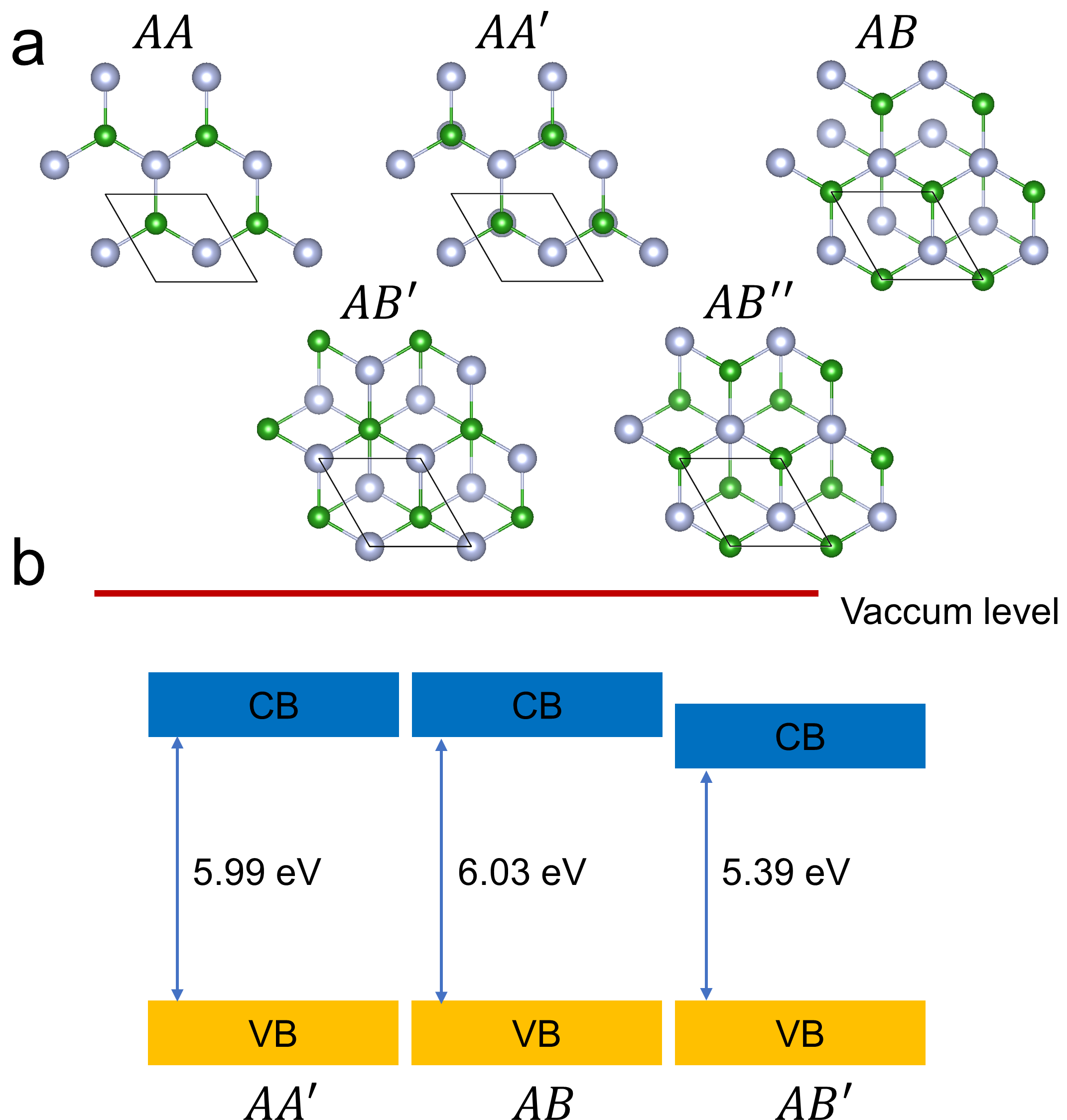
According to the stacking order of the successive sheets or layers, a bilayer of hBN can emerge in five different high-symmetry stackings Gilbert et al. (2019); Constantinescu et al. (2013), as shown in Figure 1a. First, we compared the relative stability of these sequences by computing the total energies and checking for the appearance of imaginary modes in the phonon calculations. This analysis revealed that the AA and stackings are unstable, as indicated by the presence of imaginary phonon modes at 10.4 meV and 8.3 meV, respectively. These results are consistent with a previous study that reported higher total energies for these two stacking sequences Gilbert et al. (2019). In fact, the stacking pattern is commonly observed in most synthesized hBN samples, and its properties have been extensively studied in the past decades Bourrellier et al. (2014); Kim et al. (2015); Alem et al. (2009). Interestingly, we found that the AB stacking has a lower total energy than the conventional stacking, and its presence has been confirmed by HR-TEM imaging and by combining second harmonic generation (SHG) with photoluminescence spectroscopy Warner et al. (2010); Rousseau et al. (2022a). Therefore, we focus our attention on the three stable polytypes, namely, , AB and . Our calculations were able to reproduce the experimental band gap of approximately 6.1 eV for and AB. Note that this value neglects a contribution of the zero-point renormalization, which arises from electron-phonon interactions Cassabois et al. (2016). We also observe a substantial decrease in the band gap energy to 5.3 eV for , as shown in Figure 1b. Aligned with the vacuum level, it becomes evident that the decrease in the band gap of is primarily attributed to the shift in the conduction band minima (CBM), while the valence band maximum (VBM) remains unchanged.
In the literature, several compelling models exist to accurately describe the defects responsible for single-photon emission in the ultraviolet region of hBN. These models include a 2C (CNCB) defect Mackoit-Sinkevičienė et al. (2019), as well as our recent findings on carbon complexes, and a Stone-Wales (SW) defect Hamdi et al. (2020); Li et al. (2022b). The structures and energy diagrams of these defects are shown in Figure 2. All these defects maintain a stable neutral charge state over an energy range that exceeds the ionization threshold. The 2C defect exhibits one occupied and one empty state within the band gap, both possessing a symmetry. The occupied state primarily originates from a orbital of CN, while the empty state arises from a orbital of CB. On the other hand, the 4C defect features two additional levels within the energy gap between the states, resulting in the lowest optical transition from to . In contrast to the previous defects, the 6C carbon ring exhibits a symmetry, giving rise to degenerate e states within the band gap. These states are labeled as occupied and unoccupied . Similar to the 2C defect, the SW defect also possesses one occupied and one empty defect level. Despite occasional variations in the absolute energies, the basic electronic structure of these defects remains well-preserved across different stackings. In Supplementary Fig. 2, we provide detailed defect configurations that we modeled in the three polytypes. It is worth noting that we considered two nonequivalent lattice sites for AB stacking, denoted as AB1 and AB2. In AB1 stacking, carbon atoms are aligned with nitrogen atoms, whereas in AB2 stacking, carbon atoms are aligned with boron atoms.
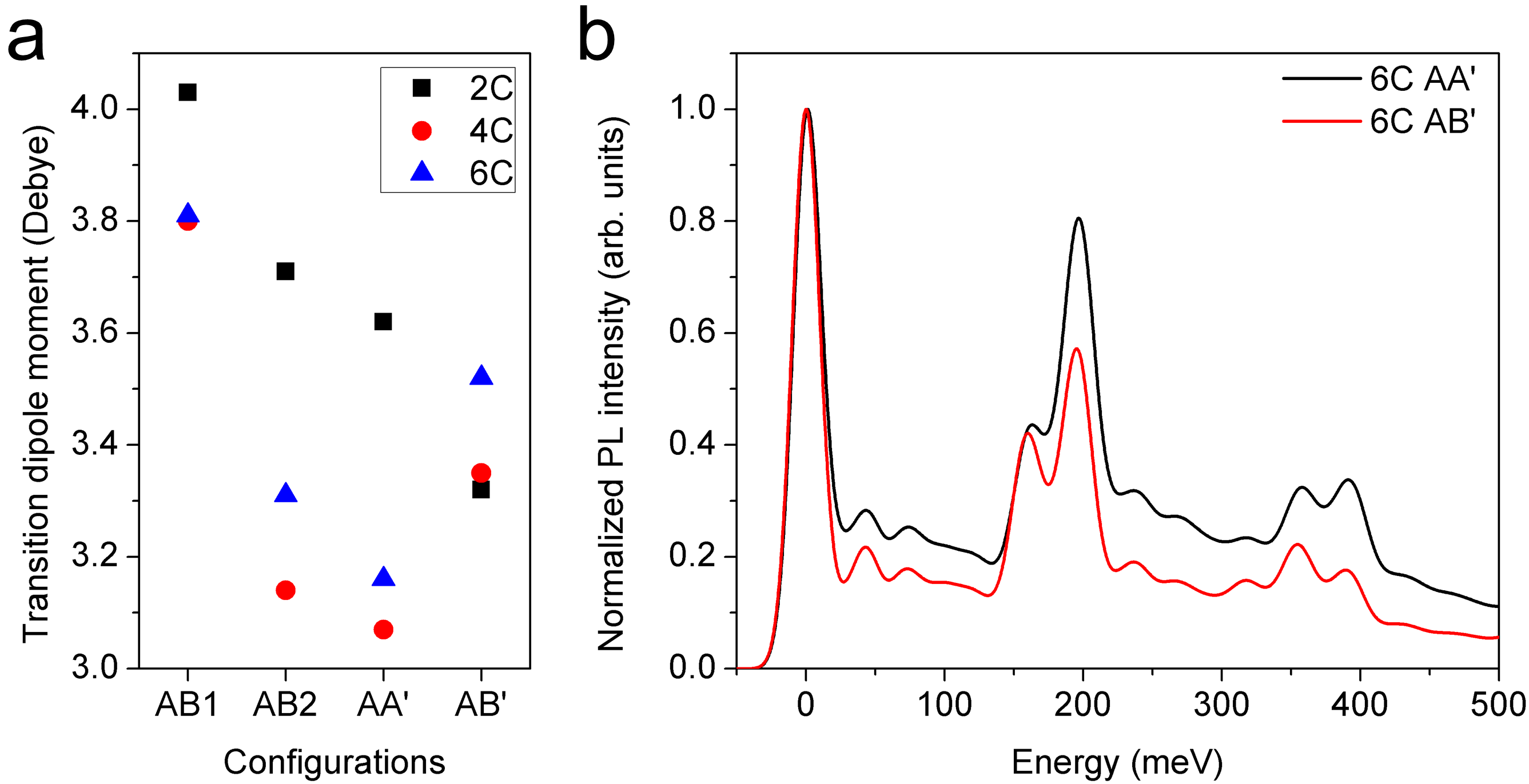
We present the calculated parameters, including ZPLs, Huang-Rhys (HR) factors, and radiative lifetimes, in Table 1. Our results show that compared to the previous work on 2C Mackoit-Sinkevičienė et al. (2019), our calculations yield lower ZPLs and longer radiative lifetimes. This difference can be attributed to the varying fraction of the Fock exchange. Importantly, we account for the two-determinant nature of the excited singlet state in our ZPL calculations through a correction term, as discussed in Supplementary Note 2. Our calculations reveal that interlayer interaction greatly impacts the photoluminescence spectrum. First, for all three carbon defects, the ZPLs increase when transitioning from to AB stacking, while the variations are found to be system-specific. In particular, 2C shows a small change in ZPL, from 4.09 eV in stacking to 4.24 or 4.21 eV with AB stacking in accordance with experimental observations Rousseau et al. (2022b). Notably, despite the substantially smaller band gap in stacking, the ZPLs only experience a slight shift. Furthermore, the stacking arrangement affects the relaxation energy in the excited state. For the 2C defect, the relaxation energy is 0.21 eV and 0.24 eV for the AB1 and AB2 configurations, respectively. This suggests a relatively stronger electron-phonon coupling with the AB1 pattern and highlights the influence of stacking on the optical transitions of defects. This effect is further demonstrated by the calculated HR factors, which increase from 1.80 to 2.02 when transitioning from AB1-2C to AB2-2C. By contrast, the changes in lifetime range from 1.5 to 3.3 ns, which, despite notable variations in the transition dipole moment shown in Figure 3a, are relatively small. This is because the increase in the dipole moment is offset by the decrease in ZPL energies. Thus, the primary effect of the stacking arrangements is the modification of the photoluminescence shape, with the narrowest signals observed in stacking. To further illustrate the concept of sideband engineering by altering the stacking sequence, Fig. 3b depicts the PL sidebands of and for the 6C defect.
| Defect | ZPL | HR factor | TDM | Lifetime |
|---|---|---|---|---|
| -2C | 4.09 | 1.94 | 3.62 | 2.59 |
| AB1-2C | 4.24 | 1.80 | 4.03 | 1.88 |
| AB2-2C | 4.21 | 2.02 | 3.71 | 2.28 |
| -2C | 4.00 | 1.68 | 3.32 | 3.32 |
| -4C | 4.32 | 1.47 | 3.07 | 3.07 |
| AB1-4C | 4.56 | 1.20 | 3.80 | 1.47 |
| AB2-4C | 4.45 | 1.58 | 3.14 | 2.39 |
| -4C | 4.28 | 1.10 | 3.35 | 2.66 |
| -6C | 4.17 | 2.09 | 3.16 | 3.22 |
| AB1-6C | 4.49 | 1.74 | 3.81 | 1.85 |
| AB2-6C | 4.31 | 1.96 | 3.31 | 2.67 |
| -6C | 4.22 | 1.56 | 3.52 | 2.34 |
| -SW | 3.99 | 3.12 | 1.59 | 14.44 |
| AB1-SW | 4.01 | 3.21 | 1.56 | 14.93 |
| AB2-SW | 3.97 | 3.62 | 1.66 | 13.29 |
| -SW | 3.97 | 2.94 | 1.85 | 10.92 |
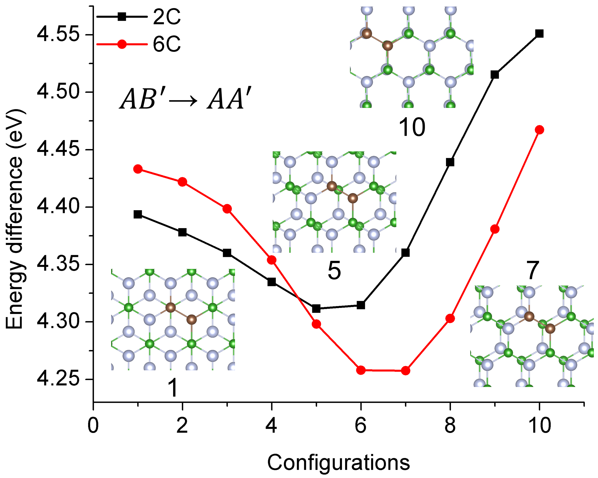
We proceed to investigate the effect of sliding which is feasible between the and configurations. Due to the rapid recovery of a high symmetry configuration (either or ), performing a full geometry optimization of the defected structures becomes cumbersome. Therefore, our focus is on the energy difference between defect levels for the sliding from to configurations, as illustrated in Fig. 4. We observe a decrease in the energy difference when the geometry is in an off-high-symmetry configuration, reaching a value within 0.25 eV. This observation suggests that the ZPLs may shift during the sliding process, as well. The evolution of the energy difference is primarily driven by the changes in the band gap of pristine hBN during sliding, as depicted in Supplementary Fig. 9. Generally, the band gap decreases with non-centrosymmetric stackings, reaching a minimum when the other layer lies on a bridge site. There is an explanation for these effects, which suggests that chemical (Coulomb) interactions play a crucial role in determining the relative stability of different stackings, while electron correlation softens the potential energy surface Constantinescu et al. (2013).
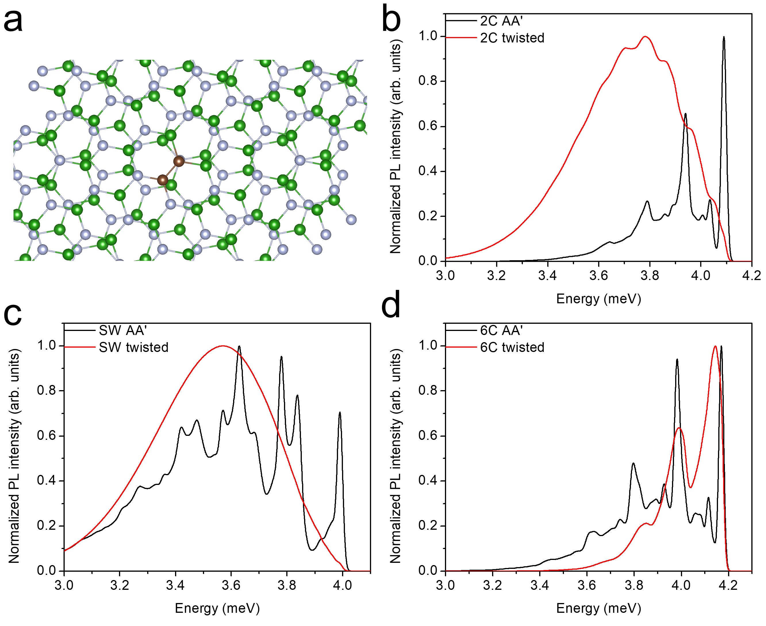
Having described the properties of single-photon emitters in different polytypes, we now shift our focus to the defect-related photoluminescence observed in twisted hBN bilayers. Unlike symmetric translations, the locally inhomogeneous environment resulting from twisting induces an out-of-plane net field. This phenomenon, in turn, can interact with the dipole moments of both ground and excited states, consequently modifying the emission spectra (also known as the Stark effect). More precisely, we examine the influence of these fields on the photoluminescence properties of 6C, 2C, and SW defects. In Fig. 5, we compare their PL sidebands calculated in the twisted bilayers and stacking. It becomes evident that the response of these defects to twisting differs remarkably. However, this effect can be understood by analyzing the computed changes in dipole moments in the ground and excited states Bilot and Kawski (1962). As confirmed by the results in Table 2, the degree of correlation between the changes in dipole moment and the HR factors is large, given that a complete relaxation toward the net fields is impeded by the hBN lattice. Specifically, the response of the 6C defect to twisting only exhibits marginal variation, while the magnitude of changes falls within the range of the effect observed in different stacking sequences. On the other hand, striking modifications are observed for the 2C and SW defects, largely due to their substantial variations in dipole moments upon excitation. It is worth noting that, due to the change in dielectric environment, the positions of the zero-phonon line remain essentially stable for each defect.
| Defect | HR () | HR (twisted) | |
|---|---|---|---|
| 6C | 2.08 | 2.69 | 0.1 |
| 2C | 1.94 | 5.60 | 0.6 |
| SW | 3.12 | 6.94 | 5.5 |
Among these defect configurations, the response of the 2C defect is particularly intriguing, as its sideband modifications align remarkably well with experimental measurements (see Supplementary Fig. 8b). Additionally, in the relaxed excited state geometry, we observe a distortion of the defect axis out of the basal plane by approximately 9 degrees. For the sake of reference, this distortion is approximately 3 degrees in the bilayer and 0 degrees in bulk. The out-of-plane distortion may have a dual effect on the observed photoluminescence intensity. Firstly, due to its alignment with the direction of the laser beam in a typical optical setup, a permanent component of the transition dipole moment () enhances both absorption and emission. Secondly, further modifications of the wavefunctions can result from an additional geometrical relaxation. By discriminating the contributions of these two effects, we obtain the enhancement of the PL intensity from the contribution by a factor of 8.9, once again aligning with experimental measurements. In turn, the total PL intensity remains rather stable suggesting that the observed effect is primary caused by the defect reorientation toward the net field. Therefore, based on a full agreement with the experimental results, we put forward the 2C defect as the primary source of the experimental response of the 4.1-eV emission observed in the twisted bilayers of hBN.
It is important to note that Su et al. Su et al. (2022) provided a different theoretical explanation for the modification of the optical signal in the twisted bilayers. However, despite utilizing an advanced electronic structure method, the authors did not consider the reorganisation of the ions consisting of the defects upon excitation. On the other hand, our calculations reveal the dominant role of the Stark effect, which appears to significantly impact the identification of defects in hBN. Moreover, these calculations offer new insights for experimentally validating the proposed mechanism. As depicted in Supplementary Fig. 8a, the interlayer twist activates vibrational modes within the energy range of 10-100 meV. Specifically, the modes at close to 20 meV are responsible for the out-of-plane distortion. We believe that these new signals could be observable in resonance Raman measurements and would further confirm the environmental modulation of intra-defect emission in hBN.
III Summary and conclusion
In summary, we propose modifying the photoluminescence response of single photon emitters in hexagonal boron nitride by altering the stacking sequences. Our calculations indicate remarkable changes in the HR factors, with variations of up to 50% observed for certain defects with regular polytypes. The dipolar defects exhibit strong coupling to the polytype, indicating a prominent role of the Stark effect. Given the general interest in SPEs with sharp emission, the stacking is expected to produce the narrowest PL signals. By introducing twisting, the effect can be further enhanced, leading to a complete transformation of the sideband shape and effectively increased brightness. Therefore, when comparing calculated spectra to experimental data, caution should be exercised given the remarkable impact of PL spectroscopy on defect identification. Our calculations for the 2C defect align particularly well with the available experimental data, suggesting that the 2C defect is likely the primary source of the 4.1 eV-emission. In turn, its exceptional signal variations could be exploited to monitor local rearrangements of hBN caused by stain, electric fields, and other perturbations. The current technique also improves the capability of photoluminescence measurements, enabling more effective identification of defect structures at large. Future investigations should focus on comprehending the coupling between defect spin properties and environmental changes in the different arrangements of hBN layers.
IV Methods
Our density functional theory (DFT) calculations were performed by the Vienna ab initio simulation package (VASP) code Kresse and Furthmüller (1996a, b) using a plane wave basis. Projector augmented wave (PAW) potentials Blöchl (1994); Kresse and Joubert (1999) were used with a cutoff energy of 450 eV. A two-layered supercell model was constructed to avoid the interactions of defect with its periodic images and to apply the -point sampling scheme. The interlayer vdW interaction was described with DFT-D3 method of Grimme Grimme et al. (2010) for the dispersion correction. To accurately account for the band gap energy, we modified the screened hybrid density functional of Heyd, Scuseria, and Ernzerhof (HSE) Heyd et al. (2003) with a mixing parameter for the Fock exchange. The geometry optimization and calculation of electronic properties were performed with the HSE functional in consistency with our previous studies. The convergence threshold for the forces was set to 0.01 eV/Å. SCF method Gali et al. (2009) was used to calculate excited states. Since the interlayer distance of different stackings does not change significantly, we fix it in our model to the value of 3.31 Å. In addition, we constructed a bilayer configuration of 252 atoms to investigate the impact of twisting on the properties of SPE. To avoid lattice mismatch between the layers Shallcross et al. (2008), we selected a twist angle of 21.79∘ which falls into a region of intensified PL signal for the 4.1 eV-emission Su et al. (2022).
The PL spectrum was simulated using the Franck-Condon approximation by computing the overlap between the phonon modes in the ground and excited states. Gali et al. (2009); Alkauskas et al. (2014). The phonon modes were calculated with the Perdew-Burke-Ernzerhof Perdew et al. (1996a) (PBE) functional, which is a widely used, reliable and time-saving approximation. The radiative lifetime was computed using the following equation:
| (1) |
where is the vacuum permittivity, is the reduced Planck constant, is the speed of light. The refractive index for hBN was chosen at the ZPL energy of around 4.1 eV.
The changes in the dipole moment upon excitation were evaluated by the time-dependent density functional theory (TDDFT) method using the ORCA code Neese (2018). To this end, a cluster model of 120 atoms was described with the cc-pVDZ basis set Dunning Jr (1989) and the PBE0 density functional Perdew et al. (1996b). The TDDFT results also confirm that the lowest excitations of the 2C and SW defects are essentially between the single pairs of orbitals, which perfectly fits into the scope of SCF method. A justification of SCF method for the 6C defect is provided elsewhere Li et al. (2022b).
Author contribution
S.L. and A.P. performed the calculations with a contribution of P.L. and wrote the paper with input from all authors. All authors discussed the results. A.G. conceived the work and supervised his group members.
Competing interests
The authors declare that there are no competing interests.
Data Availability
The data that support the findings of this study are available from the corresponding author upon reasonable request.
Acknowledgements.
AG acknowledges the Hungarian NKFIH grant No. KKP129866 of the National Excellence Program of Quantum-coherent materials project and the support for the Quantum Information National Laboratory from the Ministry of Innovation and Technology of Hungary. A part of the calculations was performed using the KIFÜ high-performance computation units.References
- Dean et al. (2010) C. R. Dean, A. F. Young, I. Meric, C. Lee, L. Wang, S. Sorgenfrei, K. Watanabe, T. Taniguchi, P. Kim, K. L. Shepard, and J. Hone, Nat. Nanotechnol. 5, 722 (2010).
- Yang et al. (2013) W. Yang, G. Chen, Z. Shi, C.-C. Liu, L. Zhang, G. Xie, M. Cheng, D. Wang, R. Yang, D. Shi, K. Watanabe, T. Taniguchi, Y. Yao, Y. Zhang, and G. Zhang, Nat. Mater. 12, 792 (2013).
- Petrone et al. (2015) N. Petrone, T. Chari, I. Meric, L. Wang, K. L. Shepard, and J. Hone, ACS Nano 9, 8953 (2015).
- Pons-Valencia et al. (2019) P. Pons-Valencia, F. J. Alfaro-Mozaz, M. M. Wiecha, V. Biolek, I. Dolado, S. Vélez, P. Li, P. Alonso-González, F. Casanova, L. E. Hueso, L. Martín-Moreno, R. Hillenbrand, and A. Y. Nikitin, Nat. Commun. 10, 3242 (2019).
- Dai et al. (2014) S. Dai, Z. Fei, Q. Ma, A. S. Rodin, M. Wagner, A. S. McLeod, M. K. Liu, W. Gannett, W. Regan, K. Watanabe, T. Taniguchi, M. Thiemens, G. Dominguez, A. H. C. Neto, A. Zettl, F. Keilmann, P. Jarillo-Herrero, M. M. Fogler, and D. N. Basov, Science 343, 1125 (2014).
- El-Kerdi et al. (2023) B. El-Kerdi, A. Thiaville, S. Rohart, S. Panigrahy, N. Brás, J. Sampaio, and A. Mougin, Nano Lett. 23, 3202 (2023).
- Gottscholl et al. (2020) A. Gottscholl, M. Kianinia, V. Soltamov, S. Orlinskii, G. Mamin, C. Bradac, C. Kasper, K. Krambrock, A. Sperlich, M. Toth, I. Aharonovich, and V. Dyakonov, Nat. Mater. 19, 540 (2020).
- Chejanovsky et al. (2021) N. Chejanovsky, A. Mukherjee, J. Geng, Y.-C. Chen, Y. Kim, A. Denisenko, A. Finkler, T. Taniguchi, K. Watanabe, D. B. R. Dasari, P. Auburger, A. Gali, J. H. Smet, and J. Wrachtrup, Nat. Mater. 20, 1079 (2021).
- Mendelson et al. (2021) N. Mendelson, D. Chugh, J. R. Reimers, T. S. Cheng, A. Gottscholl, H. Long, C. J. Mellor, A. Zettl, V. Dyakonov, P. H. Beton, S. V. Novikov, C. Jagadish, H. H. Tan, M. J. Ford, M. Toth, C. Bradac, and I. Aharonovich, Nat. Mater. 20, 321 (2021).
- Stern et al. (2022) H. L. Stern, Q. Gu, J. Jarman, S. E. Barker, N. Mendelson, D. Chugh, S. Schott, H. H. Tan, H. Sirringhaus, I. Aharonovich, and M. Atatüre, Nat. Commun. 13, 618 (2022).
- Liu et al. (2022a) W. Liu, N.-J. Guo, S. Yu, Y. Meng, Z. Li, Y.-Z. Yang, Z.-A. Wang, X.-D. Zeng, L.-K. Xie, J.-F. Wang, J.-S. Xu, Y.-T. Wang, J.-S. Tang, C.-F. Li, and G.-C. Guo, Mater. Quantum. Technol. 2, 032002 (2022a).
- Vaidya et al. (2023) S. Vaidya, X. Gao, S. Dikshit, I. Aharonovich, and T. Li, Adv. Phys.: X. 8, 2206049 (2023).
- Gottscholl et al. (2021a) A. Gottscholl, M. Diez, V. Soltamov, C. Kasper, D. Krauße, A. Sperlich, M. Kianinia, C. Bradac, I. Aharonovich, and V. Dyakonov, Nat. Commun. 12, 4480 (2021a).
- Yang et al. (2022) T. Yang, N. Mendelson, C. Li, A. Gottscholl, J. Scott, M. Kianinia, V. Dyakonov, M. Toth, and I. Aharonovich, Nanoscale 14, 5239 (2022).
- Gao et al. (2023) X. Gao, S. Vaidya, P. Ju, S. Dikshit, K. Shen, Y. P. Chen, and T. Li, arXiv preprint arXiv:2303.02326 (2023).
- Tran et al. (2016a) T. T. Tran, K. Bray, M. J. Ford, M. Toth, and I. Aharonovich, Nat. Nanotechnol. 11, 37 (2016a).
- Tran et al. (2016b) T. T. Tran, C. Elbadawi, D. Totonjian, C. J. Lobo, G. Grosso, H. Moon, D. R. Englund, M. J. Ford, I. Aharonovich, and M. Toth, ACS Nano 10, 7331 (2016b).
- Bourrellier et al. (2016) R. Bourrellier, S. Meuret, A. Tararan, O. Stéphan, M. Kociak, L. H. Tizei, and A. Zobelli, Nano Lett. 16, 4317 (2016).
- Li and Gali (2022) S. Li and A. Gali, J. Phys. Chem. Lett. 13, 9544 (2022).
- Hamdi et al. (2020) H. Hamdi, G. Thiering, Z. Bodrog, V. Ivády, and A. Gali, Npj Comput. Mater. 6, 178 (2020).
- Weston et al. (2018) L. Weston, D. Wickramaratne, M. Mackoit, A. Alkauskas, and C. G. Van de Walle, Phys. Rev. B 97, 214104 (2018).
- Li et al. (2022a) K. Li, T. J. Smart, and Y. Ping, Phys. Rev. Mater. 6, L042201 (2022a).
- Jara et al. (2021) C. Jara, T. Rauch, S. Botti, M. A. Marques, A. Norambuena, R. Coto, J. Castellanos-Águila, J. R. Maze, and F. Munoz, J. Phys. Chem. A 125, 1325 (2021).
- Sajid and Thygesen (2020) A. Sajid and K. S. Thygesen, 2D Mater. 7, 031007 (2020).
- Gao et al. (2021) S. Gao, H.-Y. Chen, and M. Bernardi, Npj Comput. Mater. 7, 85 (2021).
- Gottscholl et al. (2021b) A. Gottscholl, M. Diez, V. Soltamov, C. Kasper, A. Sperlich, M. Kianinia, C. Bradac, I. Aharonovich, and V. Dyakonov, Sci. Adv. 7, eabf3630 (2021b).
- Haykal et al. (2022) A. Haykal, R. Tanos, N. Minotto, A. Durand, F. Fabre, J. Li, J. H. Edgar, V. Ivády, A. Gali, T. Michel, A. Dréau, B. Gil, G. Cassabois, and V. Jacques, Nat. Commun. 13, 4347 (2022).
- Liu et al. (2022b) W. Liu, V. Ivády, Z.-P. Li, Y.-Z. Yang, S. Yu, Y. Meng, Z.-A. Wang, N.-J. Guo, F.-F. Yan, Q. Li, et al., Nat. Commun. 13, 5713 (2022b).
- Ivády et al. (2020) V. Ivády, G. Barcza, G. Thiering, S. Li, H. Hamdi, J.-P. Chou, Ö. Legeza, and A. Gali, Npj Comput. Mater. 6, 41 (2020).
- Sajid et al. (2020) A. Sajid, K. S. Thygesen, J. R. Reimers, and M. J. Ford, Commun. Phys. 3, 153 (2020).
- Vizner Stern et al. (2021) M. Vizner Stern, Y. Waschitz, W. Cao, I. Nevo, K. Watanabe, T. Taniguchi, E. Sela, M. Urbakh, O. Hod, and M. Ben Shalom, Science 372, 1462 (2021).
- Yasuda et al. (2021) K. Yasuda, X. Wang, K. Watanabe, T. Taniguchi, and P. Jarillo-Herrero, Science 372, 1458 (2021).
- Yao et al. (2021) K. Yao, N. R. Finney, J. Zhang, S. L. Moore, L. Xian, N. Tancogne-Dejean, F. Liu, J. Ardelean, X. Xu, D. Halbertal, K. Watanabe, T. Taniguchi, H. Ochoa, A. Asenjo-Garcia, X. Zhu, D. N. Basov, A. Rubio, C. R. Dean, J. Hone, and P. J. Schuck, Sci. Adv. 7, eabe8691 (2021).
- Wilson et al. (2021) N. P. Wilson, W. Yao, J. Shan, and X. Xu, Nature 599, 383 (2021).
- Caldwell et al. (2019) J. D. Caldwell, I. Aharonovich, G. Cassabois, J. H. Edgar, B. Gil, and D. Basov, Nat. Rev. Mater. 4, 552 (2019).
- Wang et al. (2022) X. Wang, K. Yasuda, Y. Zhang, S. Liu, K. Watanabe, T. Taniguchi, J. Hone, L. Fu, and P. Jarillo-Herrero, Nat. Nanotechnol. 17, 367 (2022).
- Woods et al. (2021) C. Woods, P. Ares, H. Nevison-Andrews, M. Holwill, R. Fabregas, F. Guinea, A. Geim, K. Novoselov, N. Walet, and L. Fumagalli, Nat. Commun. 12, 347 (2021).
- Ochoa and Asenjo-Garcia (2020) H. Ochoa and A. Asenjo-Garcia, Phys. Rev. Lett. 125, 037402 (2020).
- Zhao et al. (2020) X.-J. Zhao, Y. Yang, D.-B. Zhang, and S.-H. Wei, Phys. Rev. Lett. 124, 086401 (2020).
- Ouyang et al. (2020) W. Ouyang, H. Qin, M. Urbakh, and O. Hod, Nano Lett. 20, 7513 (2020).
- Rousseau et al. (2022a) A. Rousseau, P. Valvin, W. Desrat, L. Xue, J. Li, J. H. Edgar, G. Cassabois, and B. Gil, ACS Nano 16, 2756 (2022a).
- Rousseau et al. (2022b) A. Rousseau, P. Valvin, C. Elias, L. Xue, J. Li, J. Edgar, B. Gil, and G. Cassabois, Phys. Rev. Mater. 6, 094009 (2022b).
- Su et al. (2022) C. Su, F. Zhang, S. Kahn, B. Shevitski, J. Jiang, C. Dai, A. Ungar, J.-H. Park, K. Watanabe, T. Taniguchi, J. Kong, Z. Tang, W. Zhang, F. Wang, M. Crommie, S. G. Louie, S. Aloni, and A. Zettl, Nat. Mater. 21, 896 (2022).
- Gilbert et al. (2019) S. M. Gilbert, T. Pham, M. Dogan, S. Oh, B. Shevitski, G. Schumm, S. Liu, P. Ercius, S. Aloni, M. L. Cohen, and A. Zettl, 2D Mater. 6, 021006 (2019).
- Constantinescu et al. (2013) G. Constantinescu, A. Kuc, and T. Heine, Phys. Rev. Lett. 111, 036104 (2013).
- Bourrellier et al. (2014) R. Bourrellier, M. Amato, L. H. G. Tizei, C. Giorgetti, A. Gloter, M. I. Heggie, K. March, O. Stéphan, L. Reining, M. Kociak, and A. Zobelli, ACS photonics 1, 857 (2014).
- Kim et al. (2015) S. M. Kim, A. Hsu, M. H. Park, S. H. Chae, S. J. Yun, J. S. Lee, D.-H. Cho, W. Fang, C. Lee, T. Palacios, M. Dresselhaus, K. K. Kim, Y. H. Lee, and J. Kong, Nat. Commun. 6, 8662 (2015).
- Alem et al. (2009) N. Alem, R. Erni, C. Kisielowski, M. D. Rossell, W. Gannett, and A. Zettl, Phys. Rev. B 80, 155425 (2009).
- Warner et al. (2010) J. H. Warner, M. H. Rummeli, A. Bachmatiuk, and B. Buchner, ACS Nano 4, 1299 (2010).
- Cassabois et al. (2016) G. Cassabois, P. Valvin, and B. Gil, Nat. Photonics 10, 262 (2016).
- Mackoit-Sinkevičienė et al. (2019) M. Mackoit-Sinkevičienė, M. Maciaszek, C. G. Van de Walle, and A. Alkauskas, Appl. Phys. Lett. 115, 212101 (2019).
- Li et al. (2022b) S. Li, A. Pershin, G. Thiering, P. Udvarhelyi, and A. Gali, J. Phys. Chem. Lett. 13, 3150 (2022b).
- Bilot and Kawski (1962) v. L. Bilot and A. Kawski, Zeitschrift für Naturforschung A 17, 621 (1962).
- Kresse and Furthmüller (1996a) G. Kresse and J. Furthmüller, Comput. Mater. Sci. 6, 15 (1996a).
- Kresse and Furthmüller (1996b) G. Kresse and J. Furthmüller, Phys. Rev. B 54, 11169 (1996b).
- Blöchl (1994) P. E. Blöchl, Phys. Rev. B 50, 17953 (1994).
- Kresse and Joubert (1999) G. Kresse and D. Joubert, Phys. Rev. B 59, 1758 (1999).
- Grimme et al. (2010) S. Grimme, J. Antony, S. Ehrlich, and H. Krieg, J. Chem. Phys. 132, 154104 (2010).
- Heyd et al. (2003) J. Heyd, G. E. Scuseria, and M. Ernzerhof, J. Chem. Phys. 118, 8207 (2003).
- Gali et al. (2009) A. Gali, E. Janzén, P. Deák, G. Kresse, and E. Kaxiras, Phys. Rev. Lett. 103, 186404 (2009).
- Shallcross et al. (2008) S. Shallcross, S. Sharma, and O. A. Pankratov, Phys. Rev. Lett. 101, 056803 (2008).
- Alkauskas et al. (2014) A. Alkauskas, B. B. Buckley, D. D. Awschalom, and C. G. Van de Walle, New J. Phys. 16, 073026 (2014).
- Perdew et al. (1996a) J. P. Perdew, K. Burke, and M. Ernzerhof, Phys. Rev. Lett. 77, 3865 (1996a).
- Neese (2018) F. Neese, Wiley Interdiscip. Rev. Comput. Mol. Sci. 8, e1327 (2018).
- Dunning Jr (1989) T. H. Dunning Jr, J. Chem. Phys. 90, 1007 (1989).
- Perdew et al. (1996b) J. P. Perdew, M. Ernzerhof, and K. Burke, J. Chem. Phys. 105, 9982 (1996b).